Note: Descriptions are shown in the official language in which they were submitted.
2 1 ~2~3
SHIELDING MECHANISM FOR CIRCUIT SUBSTRATE
BACKGROUND OF THE INVENTION
FIELD OF THE INVENTION:
The present invention relates to a shielding mechanism for
forming a shield space for a circuit block on a print substrate
of a radio communication device for a satellite communication
system, a car phone system, a mobile phone system, or the like.
In particular, the mechanism comprises a print substrate
contained in a casing body for directing its surface, on which
a circuit block is surrounded by an earth pattern, toward to an
opening of the casing body. The shield space is formed for the
circuit block within the casing body by contacting a shield wall
formed on the cover with the earth pattern when the opening of
the casing body is closed with the cover.
DESCRIPTION OF THE PRIOR ART:
The recent tendency to reduce the size of radio communication
devices causes a problem of interference between transmit and
receive circuits. A transmit circuit sends information,
including speech or data, while a receive circuit receives such
information. In particular, when transmit and receive circuits
are formed on the same print substrate, interference between
- ~ 1 92903
these circuits results in significant deterioration of device
performance.
Japanese Patent Laid-Open Publication No. Hei 5-129789
discloses a conventional method for forming a shield space for
an electronic circuit block within a casing body. An earth
pattern is disposed around the electronic circuit block mounted
on the surface of a print substrate. A shield wall formed on a
metallic cover of the casing body is brought into contact with
the earth pattern when attaching the cover to the casing body.
Respective electronic circuit blocks are shielded from one
another with the shield space.
SUMMARY OF THE INVENTION
The present invention aims to provide a shielding mechanism
for a circuit substrate for reliably forming a shield space with
a simple structure.
According to the present invention, there is provided a
shielding mechanism for a circuit substrate comprising: a casing
body having an opening; a print substrate contained within the
casing body for directing its surface, on which a circuit block
is surrounded by an earth pattern, toward the opening; a cover
attached to the casing body so as to contact a shield wall with
the earth pattern when the cover closes the opening, said shield
wall and earth pattern being adapted to form a shield space for
21 929~3
the circuit block within the casing body; and guiding means
provided between the casing body and the cover so as to position
the shield wall with respect to the earth pattern on the print
substrate fixed to the casing body when the opening is closed
with the cover.
With the above arrangement, since the shield wall is reliably
positioned with respect to the earth pattern by the guiding
means, the shield wall can reliably be contacted with the earth
pattern, so that leakage from the shield space can be suppressed.
The shielding mechanism may further comprise positioning
means provided between the casing body and the print substrate
for positioning the print substrate with respect to the casing
body. The mechanism enables the reliable positioning of the
print substrate with respect to the casing body, so that
positioning by the guiding means can be improved.
The print substrate may be formed as a multi-layer substrate
incorporating an earth layer, which prevents interference between
the front and rear surfaces of the print substrate.
The shielding mechanism may further comprise a secondary
earth pattern formed on a rear surface of the print substrate for
electrically leading to the earth pattern through a through-hole
formed in the print substrate. The secondary earth pattern is
contacted by a secondary shield wall formed on the casing body
when fixing the print substrate to the casing body. The circuit
- 2 1 ~2~3
blocks on the front and rear surfaces of the print substrate is
protected from interference.
BRIEF DESCRIPTION OF THE DRAWINGS
The above and other objects, features and advantages will be
further apparent from the following description of the preferred
embodiment taken in conjunction with the accompanying drawings,
wherein:
Fig. 1 illustrates the entire structure of an electronic
device employing a shielding mechanism for a circuit substrate
according to a first embodiment of the present invention;
Fig. 2 is a perspective view illustrating an entire structure
of a cover;
Fig. 3 is a sectional view along the line 3-3 in Fig. 1;
Fig. 4 illustrates the entire structure of an electronic
device employing a shielding mechanism for a circuit substrate
according to a second embodiment of the invention;
Fig. 5 illustrates an entire structure of an electronic
device employing a shielding mechanism for a circuit substrate
according to a third embodiment of the invention;
Fig. 6 is a sectional view along the line 6-6 in Fig. 5;
Fig. 7 is a sectional view corresponding to Figs. 3 and 6,
illustrating an electronic device employing a shielding mechanism
for a circuit substrate according to a fourth embodiment of the
~1~2~o3
invention; and
Fig. 8 is a sectional view corresponding to Figs. 3 and 6,
illustrating an electronic device employing a modification of the
shielding mechanism according to the fourth embodiment.
DESCRIPTION OF THE PREFERRED EMBODIMENTS
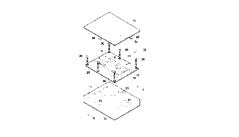
Fig. 1 illustrates an electronic device 10 employing a
shielding mechanism for a circuit substrate according to a first
embodiment of the invention. The electronic device 10 comprises
a metallic casing body 12 having an opening 11, and a metallic
cover 13 to be attached to the casing body 12 to thereby close
the opening 11 of the casing body 12. The casing body 12 and the
cover 13 together form a space containing a print substrate 14.
A plurality of circuit blocks such as a transmit circuit
block 15 and a receive circuit block 16 in a radio communication
device are mounted on the front surface of the print substrate
14, which serves as a circuit surface. The respective circuit
blocks 15, 16 are surrounded by an earth pattern 17 formed on the
print substrate 14, so that the blocks 15, 16 are isolated from
one another by the earth pattern 17. A secondary earth pattern
18 (see Fig. 3) is formed on the rear surface, serving as a
solder surface, of the print substrate 14 corresponding to the
shape of the earth pattern 17 on the front surface. The earth
pattern 17 and secondary earth pattern 18 are electrically
2 1 ~2~03
connected with each other at equal intervals via through-holes.
The print substrate 14 is fixed to the bottom of the casing
body 12 with a plurality of screws 20. A support wall 21,
serving as a secondary shield wall, is formed on the bottom of
the casing body 12 corresponding to the shape of the secondary
earth pattern 18. The support wall 21 is integrated in the
casing body 12 by molding process such as die-casting. When the
print substrate 14 is fixed to the casing body 12, the top
surface of the support wall 21 contacts the secondary earth
pattern 18. A conductive rubber 22 (see Fig. 3) at the top
surface of the support wall 21 enables a reliable and continuous
contact between the secondary earth pattern 18 and the support
wall 21.
Fig. 2 illustrates a shield wall 22 for contacting the tip
thereof with the earth pattern 17 when the cover 13 covers the
opening 11 of the casing body 12. The shield wall 22 is
integrated in the cover 13 by molding process such as die-
casting.
Referring again to Fig. 1, guiding means is provided between
the casing body 12 and the cover 13 for guiding the cover 13 with
respect to the casing body 12. The guiding means comprises a
pair of slots 23 formed on opposite side surfaces of the casing
body 12, and a pair of guide projections 24 formed on the cover
13 for advancing into the slots 23. Guiding of the guide
21~291~
.
projections 24 by the slots 23 when closing the cover 13 enables
the positioning of the shield wall 22 on the front surface of the
print substrate 14 with respect to the earth pattern 17, which
is fixed to the casing body 12. The positioning causes the top
surface of the shield wall 22 to reliably contact with the earth
pattern 17. A reliable and continuous contact can be ensured
between the earth pattern 17 and the shield wall 22 by a
conductive rubber 25 mounted on the tip of the shield pattern 22
(see Fig. 3).
The operation of the first embodiment will next be described.
The print substrate 14 is fixed to the bottom of the casing body
12 with screws as shown in Fig. 1. The position of the print
substrate 14 with respect to the casing body 12 can be observed
through the through-holes 19 provided at equal intervals on the
earth pattern 17.
The cover 13 is subsequently attached to the casing body 12
by inserting the guide projections 24 into the slots 23. The
opening 11 of the casing body 12 is closed with the cover 13.
Closing of the cover 13 causes the guiding means to position the
earth pattern 17 and the top surface of the shield wall 22. The
conductive rubber 25 at the top surface of the shield wall 22
prevents any gaps between the earth pattern 17 and the top
surface of the shield wall 22. The earth pattern 17 and the
shield wall 22 cooperate to form shield spaces for the respective
2 il 92903
circuit blocks within the casing body 12. Interfereable wave 26
irradiated from the transmit circuit block 15 is locked in the
shield space and not transmitted toward the receive circuit 16.
The press force generated by the contact of the shield wall
22 is received by the support wall 21. The print substrate 14
is held between the support wall 21 and the shield wall 22, so
that sealing ability of the shield space can be maintained even
when vibration is applied to the electronic device 10. At the
rear of the print substrate 14, the top surface of the support
wall 21 contacts the secondary earth pattern 18 through the
conductive rubber 22 so as to form a shield space.
Interefereable wave 27 irradiated from the transmit circuit block
15 on the solder side is thus locked within the shield space and
not transmitted toward the receive circuit block 16.
Fig. 4 illustrates an electronic device 30 employing a
shielding mechanism according to a second embodiment of the
invention. In the second embodiment, a positioning means is
provided between the casing body 12 and the print substrate 14
for positioning the print substrate 14 with respect to the casing
body 12. Note that the same reference characters are attached
to elements with the same function as of the first embodiment.
For example, the second embodiment employs a positioning
means comprising a positioning aperture 31 formed in the print
substrate 14, and a positioning projection 32 formed on the
2 ~ d 3
.
bottom of the casing body 12. When the print substrate 14 is
fixed to the casing body 12, the insertion of the positioning
projections 32 into the positioning apertures 31 enables fine
positioning of the print substrate 14 with respect to the casing
body 12, so that a reliable contact can be established between
the support wall 21 and the secondary earth pattern 18. In
addition, since the casing body 12 serves to improve the
positioning between the cover 13 and the print substrate 14 so
that accuracy can be further improved in positioning between the
earth pattern 17 and the support wall 21 by the guiding means.
Figs. 5 and 6 illustrate an electronic device 40 employing
a shielding mechanism according to a third embodiment of the
invention. In the third embodiment, the cover 13 is placed into
the casing body 12 along the guide recess 41 formed on the inner
surface of the casing body 12 in parallel with the print
substrate 14. The guide recess 41 and the edge of the cover 13
together constitute the aforementioned guiding means in lieu of
the slot 23 and guide projection 24. The vertical level of the
guide recess 41 serves to control contact force of the shield
wall 22. Note that the same reference characters are attached
to elements with the same function as of the first and second
embodiments.
Fig. 7 illustrates an electronic device 50 employing a
shielding mechanism according to a fourth embodiment of the
~192q~3
-
invention. In the fourth embodiment, the print substrate 14 is
constructed into a multi-layer substrate incorporating an earth
layer 51 formed therein. Specifically, an earth pattern is
formed in an intermediate layer or an earth layer 51 of the
multi-layer print substrate 14. The earth pattern is
electrically connected to the earth patterns 17, 18 on the front
and rear surfaces of the print substrate 14, respectively, via
the through-holes 19. This arrangement enables interference to
be suppressed between the front and rear surfaces of the print
substrate 14. The earth layer 51 may be constituted in more than
two layers structure as shown in Fig. 8. Note that the same
reference characters are attached to elements with the same
function as of the first, second, and third embodiments.