Note: Descriptions are shown in the official language in which they were submitted.
n v S
a 2192987
P12775
TITLE OF THE INVENTION
QUARTZ OSCILLATOR DEVICE AND ITS ADJUSTING METHOD
TECHNICAL FIELD
The present invention relates to a crystal oscillation
apparatus with built-in temperature compensation function, and a
method of adjusting this crystal oscillation apparatus.
BACKGROUND OF THE INVENTION
The crystal oscillation apparatus comprises crystal
oscillating circuit; the oscillation frequency of the crystal
oscillating circuit significantly shifts along with the change in
temperature.
In order to keep said frequency shift due to temperature
variation small, a prior art crystal oscillating circuit as
disclosed in Sapan patent publication No.Heil-265708 controls the
voltage to be applied to varactor diode, which is used as a
frequency adjusting element of crystal oscillating circuit, by
means of a control circuit.
Said prior art control circuit has following
constitution; suppose the temperature compensation has to be
performed for a,range of 130'C between -35'C and 95'C, the 130'C
range is divided into zones of 4'C and temperature compensation
-1-
' 2792987
data for each of the 4'C zones are put into respective memory
devices.
In the prior-art, data regarding the precise graduation,
temperature bias point, polarity, rough graduation and fixed
offset are necessary for each of said 4'C zones in order to
compensate the temperature shift; which data are divided into 32
control voltage setting groups of 4'C zone and are stored in
respective memory devices.
In the above described constitution, temperature is
detected by a temperature sensor, one out of the data of control
voltage setting groups corresponding to the temperature detected
is selected and picked up out of the memory device, thereby the
oscillation frequency of crystal oscillating circuit is stabilizef
against variation of the ambient temperature.
A problem with said prior art is that it needs memory
device of large memory capacity; consequently, a large size
semiconductor integrated circuits is needed to house the memory
device and control circuits to control the large memory, such
control circuits inevitably become complicated and consumes a
large power.
., Namely, in said prior art, the temperature compensation
data are prepared for each of the 4'C zones, which data are stared
in the memory of control voltage setting groups for performing the
temperature-compensation by 4'C interval from -35'C to 95'C; which
means the memory device should have a capacity large enough for
-2- -
2192987
momorizing as many as 32 control voltage setting groups, large and
sophisticated control circuits are needed to control the large
memory, as a result a semiconductor integrated circuits containing
the memory and the control circuits inevitably becomes large
sized.
Furthermore, control circuits to contrdl the memory
comprising 32 control voltage setting groups consume much power.
SUMMARY OF THE INVENTION
The present invention is to provide an apparatus with
which a semiconductor integrated circuits comprising memories and
control circuits can be made smaller, hence consuming smaller
power.
In order to implement the objective, the invented
apparatus comprises a crystal oscillating circuit, a frequency
adjusting element electrically coupled with the crystal
oscillating circuit, and a control circuit for controlling the
voltage to be applied to the frequency adjusting element; said
control circuit comprises a temperature sensor, a temperature
detecting section electrically coupled with the temperature
sensor, a'memory device electrically coupled with the temperature
detecting section, an amplifier to which the memory device and
said temperature sensor are electrically coupled, a first D/A
converter electrically intervening between said memory device and
temperature detecting section, a second D/A converter electrically
- g -
' '' 219297
intervening between said memory device and amplifier; said memory
device comprises actually-operative control voltage setting groups
counting not more than 8 groups, each of the control voltage
setting groups has in the memory a temperature detection data,
amplitude setting data, and an offset voltage data.
Under the above described constitution, the memory
contains not more than 8 units of actually-operative control
voltage setting groups, each of which groups is comprised of
temperature detection data, amplitude setting data and offset
voltage data. Therefore, a memory device having smaller memory
capacity is suffice, and a simpler control circuit can control the
memory of not more than 8 actually-operative control voltage
setting groups, as a result the size of semiconductor integrated
circuits containing the memory and control circuit is reduced.
Furthermore, the smaller memory and the simpler control
circuit can work on smaller power consumption.
BRtEF DESCRIPTION OF THE DRAWINGS
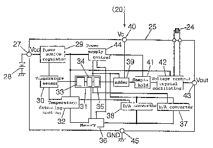
Fig.l is a block diagram of a crystal oscillation
apparatus according to an embodiment of the present invention.
Fig.2 is a block diagram of a mobile telephone using the
crystal oscillation apparatus of Fig. 1.
Fig.3 is a perspective view of a TCXO exploded used in
the crystal oscillation apparatus of Fig. 1.
-4-
2192987
Fig.4 is a block diagram of a voltage control crystal
oscillating circuit used in the crystal oscillation apparatus of
Fig. 1.
Fig.S is a circuit diagram of an amplifier used in the
crystal oscillation apparatus of Fig. 1.
Fig.6 is a circuit diagram of an adder and a sample hold
circuit used in the crystal oscillation apparatus of Fig. 1.
Fig.7 is a time chart showing the operating condition of
key part of the crystal oscillation apparatus of Fig. 1.
Fig.8 is a memory map of a memory device used in the
crystal oscillation apparatus of Fig. 1.
Fig.9 is a chart showing the control voltage applied to
baractor diode of a voltage control crystal oscillating circuit
used in the crystal oscillation apparatus of Fig. 1.
Fig.lO is a chart showing the voltage applied to
baractor diode of a voltage control crystal oscillating circuit,
and the oscillation frequency in the crystal oscillation apparatus
of Fig. 1.
BEST MODE FOR CARRYING OUT THE INVENTION
., In the following, an embodiment of the present invention
is described referring to attached drawings.
Fig.2 is a block diagram of a mobile telephone; where
numeral 1 denotes an antenna,. provided between the antenna 1 and a
receiver 2 are, from antenna 1, an antenna commoner 3, an
-5-
,i 2192981
amplifier 4, a band pass filter 5, a mixer 6, a band pass filter
7, a mixer 8, band pass filter 9, a demodulator 10, and a
receiving signal processing circuit 11. Provided between a
transmitter 12 and the antenna commoner 3 are, from transmitter
12, a transmitting signal processing circuit 13, a modulator 14, a
band pass filter 15, a power amplifier 16, and an isolator 17.
The mixer 6 is coupled with ~ VCO/synthesizer 19 via band pass
filter 18, the VCO/synthesizer 19 is coupled also with the
modulator 14. To the VCO/synthesizer 19, a control circuit 20 and
the closed~circuit of a temperature compensation type crystal
oscillating circuit(hereinafter referred to as TCXO) 21 are
coupled. The control circuit 20 is coupled with the receiving and
transmitting signal processing circuits 11, 13 and a key/display
panel 22. To the mixer 8, a crystal oscillating circuit 23 is
coupled.
A signal generated at TCXO 21 is gradually doubled at
VCO/synthesizer 19, which is supplied via band pass filter l8.to
mixer 6 of receiving system, at the same time direct to modulator
14. A diagram of such constitution is already known.
The constitution of TCXO 21 in the present embodiment is
shown in Fig.l and Fig.3. In Fig.3, numeral 23 denotes a base
. board. On top of which base board 23, a crystal oscillator 24 and
a semiconductor integrated circuits(hereinafter referred to as IC)
25 are mounted, and are covered and hermetically sealed with a
metal case 26 covering the base board 23. IC 25 is as shown in
-6
2192987
Fig.l coupled at its Vcc terminal 27 with a battery 28 of mobile
telephone shown in Fig.2. The Vcc terminal 27 is coupled also
with a power source regulator 29 for stabilizing the power supply.
The power source regulator 29 is for supplying stable
electricity to each of the parts shown in Fig. 1. A temperature
sensor 30 built within the IC 25 is coupled with an amplifier 31
and a temperature detecting section 32, and supplies the detected
temperature signal to the both_ The temperature sensor 30 is
comprised of a semiconductor diode, whose resistance value
linearly decreases along with the temperature going from the low
to high, thereby the output voltage shows a linear decrease.
The amplifier 31 is comprised of a polarity reversing
circuit 33, a'variable attenuator 34, and an amplifying circuit
35. The polarity reversing circuit 33 is coupled with temperature
sensor 30. The variable attenuator 34 is coupled with polarity
reversing circuit 33, memory 36, and second D/A converter 37.
T-
2192987
The amplifying circuit 35 is coupled with memory 36 and
variable attenuator 34. Between memory 36 and temperature
detecting circuit 32, the first D/A converter 38 is intervening.
An adder 39 is coupled with the amplifying circuit 35 of
amplifier 31. The adder 39 is coupled via Vc terminal 40 with the
control circuit 20 of mobile telephone shown in Fig.2.
The output of adder 39 is supplied via sample hold
circuit 41 to voltage control crystal oscillating circuit 42, the
output of voltage control crystal oscillating circuit 42 is
supplied via Vout terminal 43 to VCO/synthesizer 19 shown in
Fig.2.
In Fig. l, numeral 44 denotes a power supply control
section for intermittently operating the TCXO 21, which will be
described later in detail, and 45 is a grounding terminal.
The operation of TCXO 21 shown in Fig.l will be
described later in detail. For the sake of easier explanation,
the outline of operation as a whole is described here.
There are as many as 8 groups maximum of temperature
detection data, amplification setting data and offset voltage data
memorized in memory 36 as the control voltage setting group.
As soon as a temperature detected by temperature sensor
30 is supplied to temperature detecting section 32 as a first
signal, a temperature detection data among the 8 control voltage
setting groups stored in memory 36 is supplied via first D/A
converter.38 to temperature detecting section 32 one after another
-$-
2192887
as a second signal; and the first and the second signals are
compared there.
Based on the result of comparison, a decision as to
which amplification setting data and offset voltage data of
control voltage setting group among the 8 groups stored in memory
36 are to be supplied to amplifier 31 and second D/A converter 37
is made, and executed.
The execution brings about an operation for suppressing
the shift of oscillation frequency due to temperature variation.
Details of this point will be described later in a subsequent
statement.
Now in the following, the constitution of voltage
control crystal oscillating circuit 42 of Fig.l is described with
reference to Fig.4.
In the voltage control crystal oscillating circuit 42, a
stabilized DC voltage is supplied from the power source regulator
29 of Fig.l to amplifying circuits 46, 47.
An oscillating circuit is constituted with amplifying
circuit 46 and resistor 48 connected in parallel, and a crystal
oscillator 24 is oscillated by the oscillating circuit.
The oscillation output is supplied via amplifying
circuit 47 and Vout terminal 43 to VCO/synthesizer 19 of Fig.2.
In Fig.4, a plurality of baractor diodes 49 provided as
freguency adjusting element to both input and output sides of the
crystal oscillator 24 adjust the oscillation frequency. The
9-
2192987
capacitance of these baractor diodes 49 is adjusted in accordance
with the level of DC voltage applied to the cathode of baractor
diodes 49 via sample hold circuit 41 of Fig.I. Thereby the
oscillation frequency is adjusted.
In the present embodiment, the overall capacitance of
plural baractor diodes 49 disposed at the input side of crystal
oscillator 24 is made to be equal to or larger than the overall
capacitance of plural baractor diodes 49 disposed at the output
side. The reason is for reducing the power consumption; if the
capacitance at output side is larger, a larger current readily
flows resulting in a-large power consumption.
Next, the amplifier 31 is described. The amplifier 31
is comprised Of polarity reversing circuit 33, variable attenuator
34, and amplifying circuit 35, connected in series, details of
which are shown in Fig. S.
The polarity reversing circuit 33 is comprised of an
amplifying circuit 50 and two switching devices 51, 52. Each of
the switching devices 51, 52 makes opposite switching action to
each other, the amplification ratio of amplifying circuit 50 is I,
and the output of temperature sensor 30 is delivered to the
reversal input terminal of the amplifying circuit 50.
The ON and OFF operation of said switching devices 51,
52 is determined by digital data supplied from memory 36.
Namely, in a case when the switching device 51 is held
to be ON while the switching device 52 is OFF by a digital data
-1 0
292987
supplied from said memory 36, an output from temperature sensor 30
bypasses the amplifying circuit 50 to be delivered ns it is to
variable attenuator 34 via switching device 51.
Contrary to the above, when the switching device 51 is
OFF while 52 is ON, the output from temperature sensor 30 is
reversed at amplifying circuit 50 to be delivered to variable
attenuator 34. -
The variable attenuator 34 thus receiving the output
from polarity reversing circuit 33 is for controlling the
graduation by producing a preliminary graduation taking into
account the eventual graduation to be obtained after amplification
by the amplifying circuit 35.
The variable attenuator 34 comprises 16 pcs of resistors
54 connected i.n series, and a plurality of switching devices 57,
58, two respective pcs of which form one set of switch, for
guiding the voltage between the ends of a selected resistor 54 to
amplifying circuits 55, 56; wherein the selected switching devices
57, 58 are held ON at a same time.
A couple of switching devices 57, 58 is determined
depending on which NAND element 59, among several such elements,
was selected by a digital data supglied from memory 36.
As a result of the ON operation of selected switching
devices 57, 58, the voltage between both ends of a selected
resistor 54 is supplied in one end to amplifying circuit 55, and
the other end to amplifying circuit 56. -
-11-
2792987
Between the outputs of amplifying circuits 55, 56,
resistors 60 are connected in series far 16 pcs. As to which top
end of resistors 60 is selected depends on which NAND element 61,
among several such elements, was selected by a digital data
supplied from memory 36. The top end voltage of selected resistor
60 is supplied to an amplifying circuit 62.
Namely, a primary selection of voltage, e.g. 8/16 V and
7/16 V, is performed at the upper part of variable attenuator 34
shown in Fig. S, and then at the lower part of Fig.5 a secondary
voltage selection, viz which voltage value between 8/16 V and 7/16
V is to be selected, is performed by the selection of a resistor
60 among the 16 pcs.
If for example a 7.5/16 V is selected, this is supplied
to an amplifying circuit 53 via amplifying circuit 62.
As the amplification ratio of amplfying circuit 53 is
fixed at e.g. 20times, said output from amplifying circuit 62
inputted at the reversal input terminal is delivered as the output
of -20 times. Thus, the graduation, polarity of which is fixed at
said polarity reversing circuit 33, is set in this amplifying
circuit 53.
., To the non-reversal input terminal of amplifying circuit
53, an analogue voltage is supplied from second D/A converter 37;
the analogue voltage makes itself the offset voltage.
The voltage whose polarity, graduation and offset are
thus controlled at amplifier 31 is delivered to an adder 39. The
-12
2192987
constitution of adder 39 is as shown in Fig.6.
The output from amplifier 31 of Fig.5 is supplied to the
reversal input terminal of amplifying circuits 63, 64, having a xl
amplification; in a case when the oscillation frequency is shifted
due to aging or other factors, a DC voltage is supplied to Vc
terminal 40 from control circuit 20 of a mobile telephone of
Fig.2.
When said oscillation frequency is shifted to loweY
side, a DC voltage higher than a specified value is supplied to Vc
terminal 40, whereas a lower DC voltage is supplied when the
frequency is shifted to higher side.
A comparator 65 watches Whether or not a DC voltage
lower or higher than a specified value is delivered from the
control circuit 20; when such voltage is supplied to the reversal
input terminal, an OFF state is produced. Then a switching device
66 is turned ON, and 67 OFF. As a result, said DC voltage that is
. lower or higher than a specified value is supplied to the non-
reversal input terminal of amplifying circuit 64; in a case when
said lower voltage is supplied to the terminal, the voltage to be
supplied to cathode of baractor diode 49 of Fig.4 drops and the
capacitance increases, and the oscillation frequency is lowered.
Contrary, when a higher DC voltage is supplied to Vc
terminal 40, the capacitance of baractor diode 49 decreases with
the same reason as described above, and the oscillation frequency
is raised. Thus, the adder 39 prevents the shift of oscillation
-I 3- - -
,,
2192987
frequency due to aging or other causes.
Next, the output from adder 39 is delivered to a sample
hold circuit 41 as shown in Fig. f.
The sample hold circuit 41 is comprised of an amplifying
circuit 68, a capacitor 69 connected to the non-reversal input
terminal of the amplifying circuit, a switching device 70 provided
at the input side, etc.
The switching device 70 is repeated to open and close
intermittently by the power supply control section 44 shown in
Fig. l; close for l0usec, open for 310~sec, as shown in Fig.7.
While closing, the capacitor 69 is charged upto a DC
voltage level set by each of the conditions hitherto established,
and the DC voltage value to be supplied to the cathode of bsractor
diode 49 is determined by the the level of charging.
However, after the switching device.70 is opened the
voltage charged in capacitor 69 decreases due to the self
discharge. Therefore, the.switching device 70 is closed again in
310~1sec for charging.
During the switching device 70 is open, the power supply
control section 44 instructs to suspend power supply to all the
., amplifiers 31, adder 39, and first and second D/A converters 38,
37. This is intended to save the energy.
1 4-
2192987
The suspension of power supply to these parts is taken
place every time after the sample hold circuit 41 is opened, as
shown in Fig.7, thereby the capacitor 69 is charged without fail.
The memory 36 repeats predetermined routine execution.
Energy consumption is saved by the power supply control section 44
through the intermittent power supply to memory 36.
As I cycle time of routine takes 2.56msec, the 2.56msec
is made as the time for power supply to memory 36, :while the
suspension time is set to be lOsec.
The memory 36 is comprised of EEPROM, whose data are
rewritable.
In practice, there are 8 control voltage setting groups,
each group consisting of 4 b~rtes, in memory 36, as shown in Fig.8.
In each of the control voltage setting groups, a
temperature detection data is memorized in the Ist byte, a
graduation setting data in the 2nd byte, a graduation setting data
in the 3rd byte, and an offset voltage data in the 4th byte.
The first control voltage setting group represents,a
first, from low temperature side towards high temperature side,
linear control voltage(containting the polarity, graduation and
offset voltage), the second control voltage setting group a second
towards the high temperature side, the third control voltage
setting group a third towards the high temperature side, the
fourth control voltage setting group a fourth towards the high
temperature side, the fifth control voltage setting group a fifth
15-
2192987
towards the high temperature side, the sixth control voltage
setting group a sixth towards the high temperature side, the
seventh control voltage setting group a seventh towards the high
temperature side, and the eighth control voltage setting group an
eighth towards the high temperature side; in this constitution,
however, depending on the characteristics of crystal oscillator
24, the temperature compensation from the low temperature towards
high temperature side may be completed without using the entire
control voltage setting groups upto the eighth group.
Namely, the greatest feature with the present embodiment
i.s that the temperature compensation covering from the low to high
temperature range can be linear-approximated using a number of the
linear control voltages, eight at the most.
Now in the present embodiment, a case 26 is attached on
a board 23 as shown in Fig.3 to hermetically seal-in an IC 25 and
a crystal oscillator 24, then these members as they are put into a
thermostatic chamber to write data in the memory there. When, the
switching device 70 of Fig.6 is kept open.
The temperature of thermostatic chamber is raised from
-30'C gradually to 80'C; meanwhile, at each 10'C, DC voltage is
applied on baractor diode 49 via capacitor 69 and amplifying
circuit 68 of Fig.6.
In each of the 10'C zones, the control voltage with
which the oscillation frequency of voltage control crystal
oscillating circuit 42 is held constant at e.g. 12.8MHz being the
-16- ,
' 2192987
standard frequency, a.s plotted to obtain a line M of Fig.9.
Likewise, in each of the 10'C zones, the control voltage
with which the oscillation frequency of voltage control crystal
oscillating circuit 42 is held at +1PPM of the 12.8MHz is plotted
to obtain a line Y of Fig.9.
Likewise, in each of the IO'C zones, the control voltage
with which the oscillation frequency of voltage control crystal
oscillating circuit 42 is held at -1PPM of the 12.8MHz is plotted
to obtain a line K of Fig_9.
By connecting from the -30'C to 80'C so that it-falls
within an area between the lines Y and K, 5 linear control
voltages (line T) are obtained as shown in Fiq.lO.
The'first (from the low temperature) straight line of
linear control voltage line T covers a region from -30'C to -12'C,
making a straight voltage control Line connecting from 3.45V to
2.54V.
The second line covers from -12'C to +9'C, making a
straight voltage control line connecting from 2.54V to 2.33V.
The third line covers from 9'C to 43'C, making a
straight voltage control line connecting from 2.33V to 2.55V.
The fourth line covers from 43'C to 63'C, making a
straight voltage control line connecting from 2.55V to 2.35V.
The fifth line covers from 63'C to 80'C, making a
straight voltage control line connecting from 2.35V to 1.65V.
-1 7-
I
~ 2192987
The above described data corresponding to each of the 5
straight voltage control lines are written respectively in the
first to fifth control voltage setting groups of memory 36, as the
temperature detection data, graduation setting data, and offset
voltage data.
When the writing of data into memory 36 is finished the
switching device 70 of Fig.6 is restored to normal state, under
which state the open/close operation is controlled by power supply
control section 44 as described already.
And then, when the temperature of thermostatic chamber
is raised from -30'C gradually to 80'C, anode of baractor diode 49
receives from time to time according to the temperature the
control voltage (line T) of Fig.lO generated according to data
from memory 36. As a result, the oscillation frequency of voltage
control crystal oscillating circuit 42 is maintained within ~1PPM,
as shown in Fig.lO with a line H. Thus, a crystal oscillation
apparatus of very high precision is implemented.
A line L in Fig.lO represents shifting frequency of the
oscillation when the above described control voltage was not
applied to. When the line H of present embodiment is compared
with the line L, it may be understood that the accuracy of
invented apparatus is extremely high despite the fact that it is
obtained through a linear approximation with 5 straight control
voltage lines.
-1 8-
2192981
The temperature detection data of each control voltage
setting group in memory 36 is converted into DC voltage at the
first D/A converter 38 of Fig. l, and then supplied to temperature
detecting section 32 to be compared with the present temperature
detected by temperature sensor 30. As the temperature sensor is
comprised of semiconductor diode, the output voltage linearly
decreases along with the increasing temperature.
When the voltage from first D/A converter 38 is
recognized to be higher as a result of the temperature comparison,
a next sequence is executed to read out the data of control
voltage setting group.
As a result of repetition of the sequence, when the DC
voltage from temperature sensor 30 goes higher than that from
first D/A converter 38, the graduation setting data and offset
voltage data of corresponding control voltage setting group in
memory 36 are read out. Among which data, the graduation setting
data is supplied to polarity reversing circuit 33 and variable
attenuator 34 in amplifier 31 of Fig. S. The offset voltage data
is supplied to variable attenuator 34 and amplifying circuit 35 of
Fig.S via second D/A converter 37, as described already.
As described above, the present embodiment conducts a
straight line approximation with linear control voltages numbering
not more than 8. This is based on new findings that among the
voltage control crystal oscillating circuits each one circuit has
its own shape of control voltage zone (shown in Fig.9), different
1 9-
2192987
to each other, and that despite the above fact the high precision
control as accurate as ~1PPM is implementable with linear control
voltages counting as many as 8.
The finding made the grouping into 8 units of actually-
operative control voltage setting groups of memory 36 possible,
which enabled a significant down-sizing of memory device, hence
simplification and down-sizing of control circuits, further
effects include saving of energy consumption.
INDUSTRIAL APPLICABILI n
The invented apparatus comprises a crystal oscillating
circuit, a frequency adjusting elememt electrically coupled with
the crystal oscillating circuit, and a control circuit for
controlling the voltage to be applied to the frequency adjusting
element; said control circuit comprises a temperature sensor, a
temperature detecting section electrically coupled with the
temperature sensor, a memory device electrically coupled with the
temperature detecting section, an amplifier to which the memory
device and said temperature sensor are electrically coupled, a
first D/A converter electrically intervening between said memory
device and temperature detecting section, a second D/A converter
electrically intervening between said memory device and amplifier;
said memory device comprises actually-operative control voltage
setting groups counting not more than 8 units, each of the control
voltage setting groups has in the memory a temperature detection
-z o-
i i
2192987
data, amplitude setting data, and an offset voltage data.
Under the above described constitution, the memory
contains not more than actually-operative 8 control voltage
setting groups, each of which groups is comprised of temperature
detection data, amplitude setting data and offset voltage data.
Therefore, a memory device of smaller memory capacity is suffice,
and a simpler control circuit can control memories of not more
than 8 actually-operative control voltage setting groups, as a
result the size of semiconductor integrated circuits containing
the memory and control circuit can be made smaller.
Furthermore, the smaller memory and the simpler control
circuit can work on a smaller power consumption.
-2 1-