Note: Descriptions are shown in the official language in which they were submitted.
CA 02193288 2004-07-27
Circuit arrangement for operating a lamp
The invention relates to a circuit arrangement for
S operating a lamp, in particular a low-pressure discharge
lamp, according to the precharacterizing clause of Claim
1.
In such free-running circuits, the switching
elements must be supplied with drive power in time with
the switching frequencies.
To this end, known arrangements use a separate
current transformer, which is designed either as a
saturable-current (toroidal-core) transformer or as a
transformer with defined air gap (Hirschmann, W.:
"Elektronikschaltungen" Siemens AG, 1982, pages 148 and
150).
The disadvantages of an arrangement of this type
consist in that a separate, expensive wound part is
required, the manufacturing tolerances of which at the
same time have a decisive effect on the functional
parameters of the overall arrangement.
Another possibility consists in fitting additional
auxiliary windings to the resonant or current-limiting
inductor which is already required (cf. L2 in Figure 1)
and applying the control signals thereby obtained to the
gate or base inputs of the switching transistors via a
phase-shifter network (P 41 29 430.0).
The disadvantage of a circuit arrangement of this
type is that, at high DC voltage intermediate circuit
voltages, the step-type component of the voltage across
the resonant coil, caused by the switch-over of the
half-bridge switches, is very strongly superimposed on
the sinusoidal component of the voltage which is defined
by the resonant current oscillation. As a result, the
shape of the signal provided by the auxiliary windings
resembles a square-wave function more than a sine
function. The phase shifter proposed in the prior art (P
~~932aa
- 2 -
4129430.0) therefore operates only as a lag component,
the capacitor of which can no longer be discharged during
one RF period by-the sinusoidally decreasing secondary
voltage fast enough to ensure reliable switching off of
the half-bridge switches during an on-load half-cycle.
The object of the invention is to specify a
circuit arrangement, of the type mentioned at the start,
which is produced without a separate cost-intensive wound
part (saturable-current transformer, transformer with
defined air gap).
The object is achieved by a circuit arrangement
which is defined in the claims.
The invention has a large number of advantages.
The circuit arrangement according to the
invention can be produced relatively cost-efficiently,
since the circuit arrangement requires only inexpensive
wound parts whose manufacture can be fully automated.
According to the invention, the phase-shifter
circuit, known per se, which cannot deal with high DC
voltage intermediate circuit voltages, is developed
further in such a way that, even at critical voltages of
this type, stable operation of the overall arrangement
consisting of the ballast and the lamp is ensured.
An advantageous embodiment of the circuit
arrangement according to the invention is characterized
in that, in order to couple energy in from the load
circuit, the LC parallel tuned circuit can be
electrically connected to an auxiliary winding on the at
least one inductor of the load circuit through a
resistor. This coupling of energy from the load circuit
into the drive circuit using electrical connection is
simple to produce and independent of geometrical
manufacturing tolerances.
A further advantageous embodiment of the circuit
arrangemE_it according to the invention is characterized
in that, in order to couple energy from the load circuit
into the LC parallel tuned circuit, the inductor of the
LC parallel tuned circuit is only magnetically coupled to
the inductor of the load circuit, and in that a resistor
2i93~~~
- 3 -
can be connected to the LC parallel tuned circuit (cf .
Figure 2). With this magnetic coupling between the
inductor of the- LC parallel tuned circuit and the
inductor of the load circuit, it is possible to do
without the auxiliary windings on the inductor of the
load circuit, by means of which faster and less expensive
manufacturing is achieved. The conductive track layout on
the printed circuit board is furthermore simplified.
A further advantageous embodiment of the circuit
arrangement according to the invention is characterized
in that the induc-for of the load circuit has a magnetic
circuit with an incorporated air gap, and the inductor of
the LC parallel tuned circuit is configured with an
external air gap or as an air-core inductor. This embodi
went of the inductors of the LC parallel tuned circuit
and of the load circuit permits optimum magnetic coupling
and inexpensive production of these inductors.
A further advantageous embodiment of the circuit
arrangement according to the invention is characterized
in that the drive circuit consists of circuit parts
specific to the switching elements, and in that each
circuit part specific to the switching elements has the
LC parallel tuned circuit (cf. Figure 1) . Relatively fast
dimensioning of the drive components is thereby achieved.
Further advantageous embodiments of the circuit
arrangement according to the invention are characterized
in that, on the one hand, the natural resonant frequency
of the LC parallel tuned circuits of each circuit part
specific to the switching elements is the same and, on
the other hand, the LC parallel tuned circuits of each
circuit part specific to the switching elements have
identical inductors and identical capacitors,
respectively. The intended equal natural resonant fre-
quencies and inductors t= well as capacitors of the LC
parallel tuned circuits ensure symmetrical operation of
the two switching elements of the invertor arrangement.
A further advantageous embodiment of the circuit
arrangement according to the invention is characterized
CA 02193288 2004-07-27
-4-
in that the inductors of the plurality of LC parallel
tuned circuits are magnetically coupled. The magnetic
coupling of the inductors of the LC parallel tuned
circuits permits a reduction in the effect of
manufacturing tolerances (tolerances in the inductors
and capacitors) in the drive circuit.
A further advantageous embodiment of the circuit
arrangement according to the invention is characterized
in that the half-bridge arrangement is formed as two
mutually complementary transistors, and in that the
drive circuit in configured in such a way that the LC
parallel tuned circuit is connected, on the one hand, to
the connection point (half-bridge mid-point) of the two
switching elements and, on the other hand, to the two
control inputs of the switching elements which are
connected together (cf. Figure 13). In this case, one LC
parallel tuned circuit suffices for driving both
switching elements of the half-bridge, a further
switching element, for example a transformer, not being
required.
A further advantageous embodiment of the circuit
arrangement according to the invention is characterized
in that the drive circuit has a further switching
element which inverts a drive signal formed by the LC
parallel tuned circuit, and in that the drive circuit in
furthermore configured in such a way that the drive
signal of the LC parallel tuned circuit is fed to one
switching element and the inverted drive signal of the
34 LC parallel tuned circuit in fed to the other switching
element, respectively (cf. Figure 3). One advantage of
this embodiment consists in that no asymmetries occur in
the operation of the two switching elements of the
invertor or that tolerances due to manufacturing in the
components of the LC parallel tuned circuit have an
equal effect on both switching elements. The costs for
the further circuit part are partially compensated for
in that only one auxiliary winding in required on the
inductor of the load circuit. Furthermore, the switching
element TR may be designed in such a way as to
substitute for the inductor L3, L4 as well.
_ 5 - 2 ~ 93288
A further advantageous embodiment of the circuit
arrangement according to the invention is characterized
in that the drive circuit has a further circuit part
which produces at a first output a drive signal formed by
the LC parallel tuned circuit in inverted form, and at a
second output the drive signal of the LC parallel tuned
circuit in non-inverted form, and in that the drive
circuit is furthermore configured in such a way that the
control input of one switching element is connected to
one output of the switching element, and the control
input of the other switching element is connected to the
other output of the switching element (cf. Figure 4).
This achieves the further advantage that the LC parallel
tuned circuit may be at a reference potential which is
not simultaneously a reference potential of one of. the
two switching elements.
Further advantageous embodiments of the circuit
arrangement according to the invention are characterized
in that the further switching element is a transformer,
the transformer having one or more secondary windings,
and each secondary winding being assigned to at least one
switching element of the invertor. The required DC
isolation of the drive signals for the two switching
elements of the half-bridge is produced by the
transformer in simple fashion, specifically by the
secondary windings.
A further advantageous embodiment of the circuit
arrangement according to the invention is characterized
in that the resistor through which the auxiliary winding
can be connected to the LC parallel tuned circuit is
linear, non-linear or temperature-dependent. Although a
linear resistor represents the most cost-efficient
embodiment for this resistor, the use of a non-linear or
temperature-dependent resistor permits the implementation
of matching of the drive circuit to particular ambient
conditions (for example high ambient temperature) or
overall arrangement conditions (for example unusual lamp
operating voltage).
A further advantageous embodiment of the circuit
CA 02193288 2004-07-27
-6-
arrangement according to the invention is characterized
in that a series circuit consisting of a diode and a
resistor in connected in parallel with the LC parallel
S tuned circuit in such a way that the half-cycle of the
LC parallel tuned circuit during which the control
voltage at the control input of a switching element of
the invertor is negative is more strongly damped so that
the dead time of the half-bridge is extended (cf. Figure
5). One advantage of this embodiment is that the duty
ratio of the switching elements is altered in such a way
that the time for which a switching element is activated
is shorter within one period.
A further advantageous embodiment of the circuit
arrangement according to the invention is characterized
in that, between the LC parallel tuned circuit and the
switching element a further resistor is arranged which,
during the charge-transfer phase of a switching load-
reduction capacitor by transfer of the charge of this
capacitor, produces a voltage drop which counteracts the
drive voltage of the LC parallel tuned circuit so that
switching-on of the switching element during the
transfer of the charge of the switching load-reduction
capacitor is prevented (cf. Figure 6). A switching
element should not be switched an until the freewheeling
diode of a switching element carries current. This is
the case, in this embodiment of the circuit arrangement
according to the invention, if the switching load-
reduction capacitor has its charge fully transferred
after the other respective switching element is switched
off. The present embodiment makes it possible to make
the switch-on time of a switching element dependent on
the charge-transfer phase of the switching load-
reduction capacitor.
In conjunction with this, provision is furthermore
made that a diode is connected in parallel with the
further resistor in such a way that its anode is
connected to that terminal of the LC parallel tuned
circuit which is not connected to the control input of
the switching element and that the cathode is connected
to the reference potential of the switching element.
CA 02193288 2004-07-27
This diode permits fast switching-off of the switching
elements.
A further advantageous embodiment of the circuit
arrangement according to the invention is characterized
in that, between the control input of a switching
element and the corresponding LC parallel tuned circuit,
a pulse-shaping and impedance-converting quadripole is
looped in which accelerates the switching-off of the
switching element (cf. Figures 7 and 8). This achieves
an improved switch-off response of the switching
elements and thereby minimization of the switching
losses.
A further advantageous embodiment of the circuit
arrangement according to the invention is characterized
in that a voltage-dependent damping component is
arranged in parallel with the LC parallel tuned circuit
(cf. Figure 9). This damping component protects the
control input of the switching elements from a voltage
overload.
A further advantageous embodiment of the circuit
arrangement according to the invention is characterized
in that a series circuit, consisting of a Zener diode
and a resistor which is connected to the anode of the
Zener diode, is connected in parallel with the LC
parallel tuned circuit, and in that the control input of
the switching element is connected to the anode of the
Zener diode and the reference potential of the switching
element is connected to the connection point between the
resistor and the LC parallel tuned circuit (cf. Figure
10). Inserting the Zener diode achieves a seemingly
higher threshold voltage of the switching element and
thereby a reduction in the time for which the switching
element is activated by the LC parallel tuned circuit.
This time is further shortened by an advantageous
embodiment of the circuit arrangement according to the
invention which is characterized in that, in series with
the inductor of the LC parallel tuned circuit, a
parallel circuit consisting of a diode and a resistor is
arranged in such a way that the cathode of the diode and
CA 02193288 2004-07-27
-8-
a terminal of the resistor are connected to the
reference potential of the control input of a switching
element, and that the anode of the diode and the other
terminal of the resistor are connected to the inductor
of she. LC parallel tuned circuit, or the anode of the
diode and a terminal of the resistor are connected to
the control input of a switching element and the cathode
of the diode and the other terminal of the resistor are
connected to the inductor of the LC parallel tuned
circuit, as a result of which a negative DC voltage
offset, adjustable through the resistance of the
resistor, is achieved in the output voltage of the LC
parallel tuned circuit relative to the control input of
the switching element (cf. Figure 11).
A further advantageous embodiment of the circuit
arrangement according to the invention is characterized
in that a clamping resistor is inserted between the
control input of the switching element and the reference
potential for this control input, and in that, in order
to extend the dead time a resistor divider and a further
switching element are inserted between the control
output of the LC parallel tuned circuit and the
switching element, which switching element only applies
the output voltage of the LC parallel tuned circuit to
the switching element if the control voltage, formed by
the resistor divider from the control voltage of the LC
parallel tuned circuit, for this further switching
element exceeds the threshold voltage of the latter and
switches it on (cf, Figure 12). This embodiment permits
an active extension of the dead time up to a phase angle
of 90°. (relative to the drive voltage).
Finally, a further advantageous embodiment of the
circuit arrangement according to the invention is
characterized in that the threshold voltage of the
switching elements can be predetermined in such a way
that a predeterminable on-time of the switching elements
can be produced. This embodiment, in which the threshold
voltage of the switching elements may take on an
unusually high value, affords the advantage that, when
using these switching elements, which are special in so
far as regards the extension of the dead time tT, the
CA 02193288 2004-07-27
_g_
same effect can be achieved an with the other
embodiments mentioned above, but without additional
components.
The invention will now be described with reference
to the following figures, in which:
Figures 1-13 show embodiments of the circuit arrangement
according to the invention; and
Figures 14-17 show the waveform of selected voltages and
currents in the circuit arrangement
according to the invention.
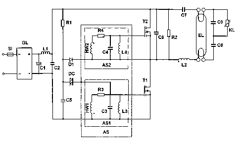
Figure 1 represents the circuit diagram of a
circuit arrangement with a push-pull half-bridge for
operating a low-pressure discharge lamp EL. Directly at
the mains input, a fuse SI is connected into a lead.
This is followed by the rectifier GL whose output is
bridged by a smoothing capacitor C1, and a radio
interference suppression component consisting of a
filter coil L1 in the positive lead and a capacitor C2
in parallel with the smoothing capacitor C1. The self-
regulating, free-running invertor, here a push-pull
half-bridge, consists of the two switching elements
(preferably MOSFET transistors or IGBT transistors with
freewheeling diode) T1 and T2 and the starting circuit
with the resistors Rl, R2, the capacitor C5, the diode
D1 and the diac DC. The lamp EL is connected, via one
terminal of the first electrode, through a resonant
inductor L2 to the centre tap between the two
transistors T1, T2, and via one terminal of the second
electrode, through a coupling capacitor C7, to the
positive pole of the capacitor C2
Furthermore, a series resonant circuit is provided,
which consists of the resonant inductor L2, the coupling
capacitor C7 and two resonant capacitors C8, Cg, the two
resonant capacitors C8, C9 being connected in series
into the heating circuit of the lamp EL. A PTC resistor
KL is furthermore connected in parallel with the
capacitor C9. In parallel with the switching path of the
transistor T2, a capacitor C6 is furthermore connected
in order to reduce the load on the switching elements.
~~93288
- 10 -
In the illustrative embodiment represented in
Figure 1, the transistors T1 and T2 are driven, in a
manner known per se, through auxiliary windings HW1 and
HW2 which are fitted to the resonant inductor L2.
According to the invention, a network, in the form of an
LC parallel tuned circuit consisting of L3 or L4 and C3
or C4 and a ballast resistor R3 or R4, is in each case
fitted between the auxiliary windings HW1, HW2 and the
gate inputs of the switching elements Tl, T2. The effect
achieved by these circuit technology measures is that the
circuit operates stably even at high voltages across the
smoothing capacitor Cl. In the illustrative embodiment
represented in Figure l, the auxiliary windings HWl and
HW2 each have the same turns number ng"1 = n~ .
In the illustrative embodiment represented. in
Figure 1, the drive circuit AS for driving the two
switching elements T1, T2 of the half-bridge comprises
two circuit parts_ASl and AS2 specific to the circuit
elements. A general provision of the invention is that
the drive circuit has at least one LC parallel tuned
circuit.
To couple energy from the load circuit, the LC
parallel tuned circuit is electrically connected or
connectable to an auxiliary winding HW1, HW2 on the
inductor L2 of the load circuit through a resistor R3,
R4.
Figure 2 represents an embodiment of the circuit
arrangement according to the invention. In this circuit
arrangement, in order to couple energy from the load
circuit into the LC parallel tuned circuit, the inductor
L3, L4 of the LC parallel tuned circuit is only
magnetically coupled to the inductor L2 of the load
circuit, a resistor R13, R14 being connectable in
parallel with the LC parallel tuned circuit. The magnetic
coupling is produced by arranging the inductor L3, L4 in
proximity to the inductor L~.
In conjunction with this, provision may be made
that the inductor L2 of the load circuit has a
magnetically closed circuit with an incorporated air gap,
CA 02193288 2004-07-27
-11-
in particular by using a corresponding core design (for
example "E-core"). The inductor L3, L4 of the LC
parallel tuned circuit is in this case configured with
an external air gap or as an air-core inductor. The
inductors L3, L4 are preferably formed by a rod-core
coi:L .
According to the invention, provision is made that
the drive circuit AS consists of circuit parts AS1, AS2
specific to the circuit elements. Each circuit part
specific to the circuit elements then has the LC
parallel tuned circuit as represented in Figures 1 and
2.
The natural resonant frequency of the LC parallel
tuned circuits of each circuit part specific to the
circuit elements is preferably the same.
Preferably, provision is also made that these LC
parallel tuned circuits of each circuit part specific to
the circuit elements each have identical inductors and
identical capacitors.
The waveform of the voltages and of the currents in
the two switching elements T1, T2 of the half-bridge
will now be described with reference to Figures 19 and
15, Figure 14 representing the voltage response U(T1,
gate), U(HW1): U{T2, gate), U(HW2) in the two drive
circuits and the corresponding transistor currents
I(T1), I(T2) during starting, and Figure 15 representing
them for a steady operating state.
As a result of initial activation of the circuit
using the Diac DC represented in Figure 1, at time ZP1
(Figure 14), the capacitor C3 charges and turns the
transistor T1 on. The voltage across the auxiliary
winding HW1 then jumps to a value defined by the turns
ratio
a - nprimary~nXWl
(=ratio of the number nPrlmary of windings on the primary
winding of the coil L2 to the number nHwi of windings on
the auxiliary winding HWl on the coil L2) and the
CA 02193288 2004-07-27
-12-
intermediate circuit DC voltage. A sinusoidal current
starts to flow in the coil L2.
The voltage across the coil L2, and therefore
across the auxiliary winding HWl, then decreases
according to
U(t)=-L~dI(t)/dt
(Time interval a between ZP1 and ZP2, Figure 14).
However, in spite of this reduction, the voltage across
the auxiliary winding HW1 remains large enough for the
capacitor C3 to be charged further through the resistor
R3. Because of the voltage across C3, a sinusoidally
increasing current starts to flow in the coil L3, which
current discharges the capacitor C3. The voltage at the
control input (gate) of the transistor Tl therefore
decreases until it is below the threshold voltage of T1
and Tl switches off (time ZP2, Figure 14).
As a result of this switching process, the resonant
current applied in the coil L2 reverses the voltage
across the inductor and therefore across the auxiliary
windings HW1, HW2. The capacitor C3 then has its charge
transferred through R3 by the voltage across HW1 and the
current applied in the coil L3 of the LC parallel tuned
circuit, and the gate voltage of T1 becomes negative.
The capacitor C4, at first negatively charged by HW2
through R4, is then charged through R4 from the
auxiliary winding HW2, since the voltage across HW2
increases abruptly when the half-bridge is switched over
(time period b between times ZP2 and ZP3, Figure 14). As
a result of the low-pass function of R4/C4, the voltage
across C4, the coil L4 and therefore also the gate of
T2, increases sinusoidally. When the threshold voltage
of T2 is exceeded, it switches on (time ZP4, Figure 14).
Because of the phase shift between the resonant current
in L2 and the gate voltage at T2, switching-on takes
place while the freewheeling diode of the switching
element T2 is carrying the resonant current (time
interval c between times ZP3 and ZP5, Figure 14).
219328
- 13
The drive voltage provided by the auxiliary winding FiW2
decreases sinusoidally, but nevertheless contributes
little or not at all to the discharging of C4.
The coil L4 then discharges the capacitor C4,
5 even though a high drive voltage is still available and
by virtue of its applied curre~at forces transfer of the
charge from C4 and therefore reliable and fast switching
off of the transistor (time ZP6, Figure 14). As a result
of the recent switch-over of the half-bridge, the
10 resonant current applied in the coil L2 reverses the
voltage across the auxiliary windings HWl and HW2 and the
primary winding. The capacitor C4 then also becomes
negatively charged through R4 by HW2, and the capacitor
C3 becomes positively charged through R3 by HWi (time
15 interval d between times ZP6 and ZP7, Figure 14). As a
result, the transistor T1 is switched on again and the
described process begins again from the start.
If the capacitor C6 represented in Figures 1-13
(in parallel, for example, with the transistor T2) is
20 used for switching load reduction, then it is necessary
for there to be a sufficient dead time tT (= time
interval b - duration of the transfer of the charge in
the capacitor C6) between the switching-off of one half-
bridge transistor and the switching-on of the other.
25 In the normal case (switching load-reduction
capacitor C6 has conventionally used capacitances) this
dead time is provided by the fact that the voltage falls
below the threshold voltage of one transistor before the
output voltage of the associated drive circuit becomes
30 zero, whereas the output voltage, symmetrical thereto, of
the other drive circuit must rise to the value of the
threshold voltage of the transistor to be switched on
before the latter actually turns on.
Figure 15 shows the voltage and current waveforms
35 of the currents in the Hitching elements Tl, T2 and the
voltages ~in the auxiliary windings and the control
voltages of the LC parallel tuned circuits when the
overall arrangement is in a steady operating state. It
can be seen that the said voltage and current waveforms
2 ~ ~~zas
- 14 -
of the drive circuits specific to the switching elements
have symmetrical profiles.
In practice, the elements of the LC parallel
tuned circuit which are represented in Figure 1 are
5 subject to non-negligible manufacturing tolerances. These
have an effect primarily if the natural resonant
frequencies
__ 1
e8 2 '7~ L3 4 ' 3 4
of the two drive circuits (AS1, AS2) differ greatly,
because mutually symmetrical drive voltage waveforms in
10 the two drive circuits AS1 and AS2 can then no longer be
assumed.
Embodiments of the circuit arrangement according
to the invention which, in particular, are represented in
Figures 5, 6, 10, 11 and 12, increase the achievable dead
15 time when switching over the half-bridge by delayed
switching-on of the transistors, in order to ensure full
transfer of the charge in the switching load reduction
capacitor C6 by the freewheeling energy stored in the
inductor L2.
20 In the embodiment of the circuit arrangement
according to the invention which is represented in Figure
5, a series circuit consisting of a diode~D3 or D4 and a
resistor R5 or R6 is respectively connected in parallel
with'each of the two. LC tuned circuits in such a way that
25 only the negative half-cycle (negative gate voltage) of
the oscillation of the LC tuned circuit is damped.
This leads to a deformation of the drive voltage
curve, which has a shorter positive half-cycle with
higher amplitude and a longer negative half-cycle with
30 lower, amplitude, and a shift in the duty ratio is thereby
achieved. '
A further embodiment of a switch-on delay, which
may also supplement the circuit arrangement described
above with reference to Figure 5, is represented in
35 Figure 6.
- 15 -
In this circuit arrangemeat, the current in the
switching load-reduction capacitor C6 is received by two
resistors (R7, R8). To this end, a series circuit
consisting of two resistors R7, R8 and the capacitor C6
5 is connected in parallel with the transistor.Tl in such
a way that one resistor (R8) is at the earth potential,
and the o~her resistor (R7) is connected to the
connection point of the two switching transistors T1, T2,
and that the capacitor ~C6 is connected between the two
10 resistors R7, .R8. A diode D7, D8 whose anodes are
connected to the respective terminal of the switching
load-reduction capacitor C6 is connected in parallel with
each of the resistors R7, R8.
In the circuit arrangement represented in Figure
15 6, the LC parallel tuned circuits are not connected in
parallel with the gate-source path of the transistors T1,
T2, but are connected via one terminal to the gate of the
respective traasistor and via the other to the cathode of
the diodes D7 (L4, C4) and D8 (L3, C3) .
20 When the transistor T1 is switched on, the
switching load-reduction capacitor C6 is discharged. If
the gate voltage of T1 then falls below the specified
threshold value, Tl switches off. This leads to charging
of C6 and a voltage drop across R7 and R8.
25 Switching-on of T2 is then delayed in that the
voltage drop across the resistor R7 due to the
discharging process of C6 is subtracted from the drive
voltage for. T2, which is delivered by the drive circuit
consisting of L4, C4, R4 and HW1.
30 The voltage drop across R8, which counteracts the
switching-off of T1 and which would therefore cause very
high-loss switching, is limited by the diode D8 to its
forward voltage.
When the gate voltage of T2 falls below its
35 threshold value, then T2 switches off, and the capacitor
C6 is discharged again through the resistors R7 and R8 by
the current applied in the coil L2. The voltage drop
across R7 is then limited by the diode D7 to its forward
voltage and the voltage across R8 is subtracted from the
2~~3288
- 16 -
voltage delivered by the drive circuit arranged at the
transistor Tl; switching-on of Tl is thereby delayed.
The resistor R3, R4 or R13, R14 (Figure 5) may be
linear, non-linear or temperature-dependent. It is
5 thereby possible to make the driving of the two switching
elements dependent on ambient conditions or overall
arrangement states. By way of example, provision may be
made that, at very high ambient temperatures, the power
consumption of the overall arrangement is reduced by the
10 resistance of the resistor R3, R4, R13, R14 becoming
smaller in proportion with an increase in the
temperature.
The use of a non-linear resistor may be provided
if the drive circuit is intended to react to
15 extraordinary operating states (such as an operating
voltage which is unusually high in mass production of the
lamp) of the overall arrangement in such a way as to
ensure reliable operation even under exceptional condi-
tions.
20 Figures 3 and 4 represent further embodiments of
the circuit arrangement according to the invention. In
this circuit arrangement, the drive circuit AS has a
further switching element TR which inverts a drive signal
formed by the LC parallel tuned circuit. This further
25 switching element TR is preferably a transformer, it
being possible for this transformer to embody the
inductors L3, L4 of the LC parallel tuned circuit. The
drive circuit is furthermore configured in such a way
thab the drive signal of the LC parallel tuned circuit is
30 delivered to one switching element (for example T1) and
the inverted drive signal of the LC parallel tuned
circuit is delivered to the other switching element (for
example T2), respectively. This produces no asymmetries
in the operation of the two switching elements of the
35 invertor. Tolerances due to manufacture in the components
of the LC parallel tuned circuit have equal effects on
both switching elements T1, T2.
As represented in Figure 4, the drive circuit may
be configured in such a way that the control input of one
- 1' -
switching element (for example Tl) is connected to one
output of the further switching element TR, and the
control input of the other switching element (for example
T2) is connected to the other output of this further
5 switching element TR. The LC parallel tuned circuit is at
a reference potential which is not at the same time a
reference potential of one of the two switching elements
Tl, T2.
As mentioned, the further switching element is,
10 for example, a transformer, the transformer having one or
more secondary windings. Each secondary winding is
assigned to at least one switching element of the
invertor. With the transformer, the required DC isolation
of the drive signals for the two switching elements T1,
15 T2 of the half-bridge is produced in simple fashion by
the secondary windings.
Figures 7 and 8 show embodiments of the circuit
arrangement according to the invention in which a pulse-
shaping and impedance-converting quadripole VP is looped
20 in between the control input of the switching element Tl,
T2 and the corresponding LC parallel tuned circuit. This
quadripole accelerates the switching-off of the switching
element Tl, T2.
In the circuit arrangement according to Figure 7,
25 the pulse-shaping or impedance-converting quadripole VP
is designed as a clearing network with two diodes and one
small-signal bipolar transistor.
The circuit variant shown in Figure 8 uses a
MOSFET transistor and a diode.
30 As a result of the establishment of an off-state
voltage when the drive voltage of the LC parallel tuned
circuit decrea8es, the diode of the quadripole VP, which
diode is connected between the LC parallel tuned circuit
and the control input of the switching element T1, T2,,
35 forms _ne threshold voltage which switches on the
respective small-signal transistor of the quadripole VP.
The input capacitor of the switching element Tl, T2-is
thereby abruptly discharged and the switching element is
switched off.
_ 219388
In the bipolar embodiment of the quadripole
(Figure 7), the further diode prevents undesired flow of
current through the base-collector diode of the small-
signal transistor.
5 Figure 9 shows a further embodiment of the
circuit arrangement, a voltage-dependent damping
component DG (preferably two Zener diodes connected in
anti-series) being arranged in parallel with the LC
parallel tuned circuit in order to limit the control
10 voltage of the switching element T1, T2. This arrangement
achieves overvoltage protection for the control input of
the switching elements.
As represented in Figure 10, as an alternative or
in addition to the embodiments described above, a Zener
15 diode ZD and a resistor RZ may be connected between the
control input of the switching element Tl, T2 and the LC
parallel tuned circuit, in such a way that the Zener
voltage is added to the threshold voltage of the
switching element and only a higher drive voltage of the
20 LC parallel tuned circuit leads to switching-on of the
switching element Tl or T2.
A particularly inexpensive drive circuit AS is
represented in Figure 13. By virtue of the use of two
mutually complementary switching elements (i.e.: T1 is a
25 p-channel MOSFET and T2 is an n-channel MOSFET) it is
sufficient to produce a common drive voltage for both
switching transistor . The switching element T2 is
activated by the positive half-cycle of the drive voltage
of the LC parallel tuned circuit, and the switching
30 element T2 is activated by the negative half-cycle. A
dead time (both switching elements switched off) is
automatically provided by the fact that both switching
elements are switched off for drive voltage values whose
magnitude is less than the threshold voltage of the
35 switching elements.
Whereas, in the circuit arrangement according to
the invention in accordance with Fig.- 5, a temporal
stretching of the negative half-cycle of the drive
voltage of the LC parallel tuned circuit is achieved, in
CA 02193288 2004-07-27
-19-
contrast thereto it is possible with the circuit
arrangement according to the invention in accordance
with. Figure 11 to achieve a DC voltage offset of the
drive voltage of the LC parallel tuned circuit, so that
the amplitude of the positive half-oscillation is less
than that of the negative one.
In the embodiment according to Figure 11, a
parallel circuit consisting of a diode D9/D10 and a
IO resistor R9/R10 is connected in series with the inductor
L3, L4 of the LC parallel tuned circuit in such a way
that the cathode of the diode D9/D10 and one terminal of
the resistor R9/R10 are connected to the reference
potential of the control input of the switching element
IS Tl, T2. The anode of the diode D9/D10 and the other
terminal of the resistor R9/R10 are connected to the
inductor L3, L4 of the LC parallel tuned circuit.
As an alternative to this, the anode of the diode
D9/D10 and one terminal of the resistor R9/R10 are
20 connected to the control input of the switching element
T1, T2, and the cathode of the diode D9/D10 and the
other terminal of the resistor (R9/R10) are connected to
the inductor L3, L4 of the LC parallel tuned circuit,-
This achieves a negative DC voltage offset U (T1,
25 gate), U (T2, gate), adjustable through the resistance
of the resistor R9, R10, in the output voltage of the LC
parallel tuned circuit relative to the control input of
the switching element T1, T2, and thereby a shortening
of the positive pulse width, for equal period, which
30 leads to activation of the switching element.
Figure 16 shown the relevant voltage waveforms as a
function of time for the circuit arrangement represented
in Figure 11. In this came, Figure 16a shows the
waveform of U(T1, gate), U (T1, gate) and U(HWl), and
35 Figure 16b shows the waveform of U(T2, gate), U (T2,
gate] . U (Tx, gate) denotes the average over time of the
drive voltage U (TX, gate) of the switching elements Tl,
T2) . Since, across a coil, it is only possible for a DC
voltage to occur Which is produced across its ohmic
40 impedance by a current flowing through the coil, the
CA 02193288 2004-07-27
-20-
voltage drop across the inductor of thy LC parallel
tuned circuit (L3, L4) has the time average UL = OV. By
virtue of the parallel connection of a diode D9/D10,
only a negative voltage can occur as the time average
across the resistor R9/R10, and, on the basis of
Kirchhoff's voltage law, this voltage is compensated for
by a DC voltage in the capacitor C3, C4 of the LC
parallel tuned circuit, superimposed on the AC voltage
U~(t).
On the basis of Kirchhoff's laws, the arrangement
of the parallel circuit of R9/R10 and D9/D10 and of the
inductor of the LC parallel tuned circuit (L3, L4)
within the series circuit is arbitrary.
By virtue of this superimposed DC voltage, a
control signal is set up, at the control input of the
half-bridge circuit elements, the duty ratio of which is
less than 50~ relative to a voltage sufficient to switch
on the half-bridge switching elements. This is
represented in Figure 16. The time average of the
control voltage of the drive circuit parts ASl and AS2
configured according to Figure 11 is negative, the
amplitude of the positive half-cycles having a smaller
magnitude than the amplitude of the negative half
cycles .
A further circuit arrangement which lengthens the
dead time t.r (both tT ; half-bridge switching elements
T1, T2 switched off), is represented in Figure 12. The
relevant voltage waveforms for a circuit according to
Figure 12 are shown by Figure 17, Figure 17a
representing U(HW1), U(T1, gate) and U(L3), (T1, gate),
while Figure 17b represents U(HW2), U(T2, gate) and
U(L4) (T2, gate).
In the circuit arrangement represented in Figure
12, a clamping resistor RK1, RK2 is inserted between the
control input of a switching element T1, T2 and the
reference potential for this control input. In order to
lengthen the dead time (tT ; T1, T2 switched off), a
resistor divider (Rsiiss /Rs2isa) and a further switching
element T3, T4 are inserted between the control output
of the LC parallel tuned circuit and the switching
element (T1, T2).
The switching element T3, T4 used is preferably
_ 21 _ z ~ 93zss
a pnp transistor which is inserted into the control line
(gate line) of the switching element Tl, T2.
As an alternative to this, the switching element
T3, T4 used may be an npn transistor which is inserted
5 into the line of the reference potential of the control
input (source) of the switching element T1, T2, in such
a way that the collector of T3, T4 is connected to the
switching element T1,-T2, the emitter to the LC parallel
tuned circuit and the base to the centre tap of the
10 voltage divider (RS1,RS2;RS3,RS4).
The drive voltage of the LC parallel tuned
circuit is in this case not applied to the switching
element T1, T2 until the control voltage, formed by the
resistor divider RS1/S3~RS2/S4 from the control voltage of
15 the LC parallel tuned circuit, for the switching element
T3, T4 exceeds the switch-on threshold (threshold
voltage) of T3, T4 and switches them on (Figures 12 and
17) .
The control transistor T3, T4 is thus connected
20 between the output of the LC parallel tuned circuit and
the control input of the half-bridge switching element
T1, T2. If the control transistor T3, T4 is off, then the
control voltage of the half-bridge switching element T1,
T2 is 0 volt. In this case, the resistor RR1~RR2 prevents
25 charging of the gate-source capacitance (input capacitor
of the switching element Tl, T2) and thus unintentional
switching-on of the half-bridge switching element T1, T2
due to extraneous influences.
If the drive voltage of the LC parallel tuned
30 circuit then increases, then the voltage drop across the
resistor divider Rsl/s3~Rs2/s4 also increases. By selection
of the ratio Rsi/s3 to Rs2/s4~ it is then possible to set
the output voltage of the LC parallel tuned circuit at
which the voltage drop across the control resistor Rsi/s3
35 becomes large enough to switch on the control transistor
T3, ,T4. At this operating point, the voltage across Rsi
or Rs3 must be just as great as the threshold voltage of
the control transistor T3, T4 (about 0.6 volt in the case
of a small-signal bipolar transistor).
2I932$8
- 22 -
The further-increasing output voltage of the LC
parallel tuned circuit is then forwarded via the switch-
on control transistor T3, T4 to the control input of the
half-bridge switching element T1, -T2 albeit less the
5 forward voltage of the control transistor T3, T4. This
leads to switching-on of the half-bridge switching
element T1, ~2. The resistor RRl/Rx2 is selected to have
a resistance high enough to have no significant effect on
the control voltage, or to place only comparatively
10 little load on the LC parallel tuned circuit.
The control transistor remains switched on until
the voltage across the control resistor Rsllor R53 falls
back below the threshold voltage and the base-collector
diode of the control transistor is fully cleared.
15 The half-bridge switching element switches. off
reliably, independently of the clearing phase of the
control transistor T3, T4', since the drive voltage of the
LC parallel tuned circuit becomes less than the control
voltage of the half-bridge switching element T1, T2
20 required for switching on.
As described above, the control transistor T3, T4
can also be inserted into the line of the reference
potential of the control input of the half-bridge circuit
element. In this case, the values for the resistor
25 divider Rs1/s3/Rs2/s4 are selected in such a way that the
voltage drop across the resistor of the voltage divider,
which is connected between the base and emitter of T3/T4,
leads to switching-on of the control transistor T3, T4.
Figure 13 shows a circuit arrangement according
30 to the invention, in which the half-bridge arrangement is
formed by two mutually complementary transistors Tl, T2.
The drive circuit AS is configured in such a way that the
LC parallel tuned circuit is connected, on the one hand,
to the connection point (half-bridge mid-point) of the
35 two sw~tching elements T1, T~2 and, on the other hand, to
the two switching-element control inputs which are
connected together. In this embodiment, one LC parallel
tuned circuit is sufficient for driving both switching
elements Tl, T2 of the half-bridge, a further switching
- 23 - 2 ? 93288
element, for example a transformer, not being required.
The circuit arrangements described above are
preferably equipped with a half-bridge arrangement,
although other common free-running invertors, for example
5 asymmetric half-bridge, full-bridge, push-pull or even
single-transistor converters, may be employed.
The circuit elements for a circuit arrangement
according to Figure 1 for operating a lamp with a power
consumption of 20 watts from a 230 volt AC network are
10 compiled below:
SI ELDUR:KPSO 3/46
GL lA, 600V
C1 lO~CF, 350V electrolytic capacitor
C2 220nF, 350V, I~tT
15 C3/C4 3.3nF, 63V, I~tT
C5 100nF, 63V, 1~BCT
C6 lnF, 630V, 1~P
C7 47nF, 350V, I~CT
C8 lOnF, 500V, I~T
20 C9 4.7nF, 630V, 1~CT
Ll rod-core coil l.5mH
L2, HW1, 8W2 Lprim ~ 2 6 mH; nprim 240.5: aHwl/2
18; EF16
L3/L4 rod-core coil 4.7mFi
R1 470k tI, 0.6W
25 R2 470k it 0.6W
R3/R4 2.2k~, 0.6W
~i~3238
- 24 -
RL Siemens PTC S1380
Tl/T2 - FET 500V, 6Q; SSUlN50, STR2N50
D1 1N4004, 1N4005, 1N4006, 1N4007
DC Diac DB3N (SGS-Thomson)