Note: Descriptions are shown in the official language in which they were submitted.
~ WO~6/01010 2 1 9 3 6 8 6 PCT~S95~7~s3
CURRENT SOURCE GATE DRIVE CIRCUIT FOR
SIMULTANEOUS FIRING OF THYRISTORS
Brief DescriPtion of the Invention
This invention relates generally to the operation
of thyristors in power conditioning devices such as
static VAR compensators. More particularly, this
invention relates to a current source gate drive circuit
operated on the low-voltage side of a power conditioning
device to produce a uniform current source pulse stream
for the simultaneous firing of thyristors within the
power conditioning device.
Backaround of the Invention
Solid state power electronics are used in
conjunction with high voltage transmission lines to
improve system performance. Operations to improve
system performance include power factor correction,
voltage regulation, and resonance damping. These
operations are executed as solid state power electronic
devices rapidly switch high voltage capacitors and
inductors. This switching operation is realized by
several thyristor power semiconductors connected in
series so as to withstand the maximum expected line
voltage. Each thyristor is switched on ~y injecting a
current into its gate-cathode junction. In a series
string of thyristors supporting a large voltage at the
time of switching, all thyristors must conduct
simultaneously to prevent overvoltage destruction of the
slower thyristors.
WO 96~01010 ~ 1 9 3 ~ . IIU..,_ ~ J~
--2--
Thyristor activation is commonly achieved with a
voltage isolation transformer with a winding operating
on the high-voltage side of the power electronic device.
The current gate drive signal is then produced with a
resistor positioned between the thyristors and the
secondary side of the voltage isolation transformer.
There are a number of problems with this voltage source
gate drive arrangement. First, it is difficult to
obtain uniform gate pulses at each thyristor because of
the normal variations in thyristor gate ;~pe~nr~s, and
because one or more thyristors may fail, thereby
resulting in a shorted gate. Second, the magnitude and
other parameters of voltage-sourced pulse trains are
controlled at the high voltage-side of the system.
Consequently, each thyristor may require costly and
complicated equipment such as a power supply, inverter,
and feedback loop for current control. Third, isolation
of the high-voltage thyristor circuit from the low
voltage control circuit is costly and bulky. It would be
highly desirable to develop a thyristor gate drive
device that provides uniform gate pulses, regardless of
variations in thyristor ; -~n~e or the presence of
failed thyristors. It would also be desirable to
develop a thyristor gate drive device that operates at
Z5 low voltage and thereby eliminates the requirement for
costly and complicated high-voltage side control
devices. Naturally, if a low voltage-side thyristor
gate drive device is to be used, it should have a simple
and ine~pensive isolation mechanism from the high-
voltage side of the power conditioning apparatus.
Current pulse shaping circuits for thyristors areactivated with edge-triggered logic. Edge-triggered
logic is susceptible to activation by noise spikes,
cross-tal~., and other transients. I~ an edge-triggered
logic device erroneously fires a thyristor, a large
differential voltage may exist across the switch at the
point of firingv For instance, in the case of a
thyristor switched capacitor, the capacitor may be
~ WO96101010 2 1 9 3 f~ A Cl/u~ a~
--3--
negatively charged to the negative-peak line voltage and
then be switched on during the positive-peak line
voltage. In this case, the capacitor will encounter a
rapid voltage change. This results in extremely high
currents which can damage the thyristors and the
capacitor.
In addition to the problem of high current due to
misfiring, the inductance of the power line and the
capacitance from the capacitor form an LC circuit with a
step input of twice the peak line voltage. The
capacitor will therefore encounter peak voltages of up
to 3 times the nominal peak line voltage, which can
eventually cause the capacitor itself to fail. Since
failed capacitors tend to form short circuits, the
associated thyristors may then have to interrupt the
full fault current of the line, which can destroy the
thyristors.
The problem of false triggering of edge-triggered
logic has previously been addressed with shielding of
critical signal lines and by minimizing imperfections in
grounding. Unfortunately, these efforts have only
incrementally improved the false firing problem and
thereby have not substantially eliminated the
phr~n~ . Therefore, it would be highly desirable to
provide a technique for eliminating the problem of false
thyristor gate firing signals.
Summarv of the Invention
A current source gate drive circuit for
simultaneous firing of a set of series or parallel
thyristors is described. The circuit includes two
current loops, each of which serves as a current
~ transformer primary. Electrically insulating tubes
enclose the current loops. Current transformer cores,
around which are wound a certain number of secondary
turns, surround the current loops, thus magnetically
coupling the primary current of the current transformer
to the secondary turns. Thyristor gate driver circuits
WO96101010 ~ 6 $ ~ PCT1US95/~)7
-4-
are electrically coupled to the current transformer
cores. Each of the thyristor gate driver circuits
receives and rectifies ac current signals from the
current loops and forms a current pulse train firing
signal. Each thyristor gate driver circuit has a
corresponding thyristor that is fired by the current
pulse train firing signal. The thyristors operate at a
high voltage, but are electrically isolated from the
current loops by the insulating tubes. A current pulse
shaping circuit is connected to the current loops and
uses dual resonant LC circuits to generate ac current
signals. The current pulse shaping circuit operates in
a low voltage region and is electrically isolated from
the high voltage region by the insulating tubes. The
current pulse shaping circuit is activated by an edge-
triggered signal. To prevent misfiring of the
thyristors, thyristor firing command logic is used to
generate a level-trigger signal. Level-triggered logic
is responsive to the level-trigger signal, but not noise
or transients, and produces a pulse train enable siqnal
that allows the thyristors to be fired.
Brief ~escriPtion of the Drawin~s
For a better understanding of the nature and
objects of the invention, reference should be made to
the following detailed description taken in conjunction
with the accompanying drawings, in which:
FIGURE l illustrates a static VAR ~1 ns~tor that
may incorporate the techniques of the present invention.
FIGUR~ 2 illustrates the , .n~ntc of the
invention and their relationship to a series thyristor
string of the static VAR compensator of Figure l.
FIGURE 3 is a more detailed depiction of the
relationship of the components of the invention to a
series thyristor string of the static VAR compensator of
Figure l.
FIG~RE 4 illustrates the current pulse shaping
circuitry of the present invention.
2 1 ~i 7; ' ~3 ~
WO 96101010 ! ~ . ID~
--5--
FIGURE 5 shows the current pulse generating
circuitry of the invention.
FIGURE 6 depicts control signals and waveforms
formed in accordance with the current pulse generating
5 circuitry of Figure 5.
FIGURE 7 illustrates a thyristor gate driver that
may be used in accordance with the invention.
FIGURE 8 shows the capacitor charge circuit of the
invention.
FIGURE ~ illustrates timing signals and waveforms
associated with the current pulse generating circuitry
of the invention.
FIGURE 10 shows the relation of the noise lock-out
circuitry to the other elements of the invention.
FIGURE 11 illustrates the details of one P~ho~;-?nt
of the level-triggered logic circuitry of the invention.
~ ike reference numerals refer to corresponding
parts throughout the several views of the drawings.
20 Detailed DescriPtion of the Invention
Figure 1 illustrates a static VAR compensator 20
that may successfully utilize the current source gate
drive circuit of the invention. The invention will be
disclosed in relation to the static VAR compensator of
25 Figure 1, however, it will be appreciated that the
invention is applicable to any power conditioning device
that uses multiple semiconductor devices.
Multiple semiconductor devices are frequently
necessitated in power electronics where switching is
required at voltages beyond the rating of individual
semiconductors. In this case, the semiconductors are
stacked to achieve the re~uired voltage blocking
capability.
A static VAR compensator (SVC) is used to switch
35 capacitors on line or to phase-angle-fire a reactor
across the line, thereby controlling either the
displacement power factor upstream of the SVC or the
line voltage at the SVC. Figure 1 illustrates a number
WO96~1010 ~ 9 '~ 6 ~ k
of - -ncating capacitors 30A, 33B, 30C, and 30D of an
SVC. Series thyristor strings 32A, 32B, 32C, and 32D
are used to switch the respective compensating
capacitors. Preferably, each series thyristor string 32
includes an isolating inductor 34, to limit in-rush
current.
Each series thyristor string 32 includes a number
of opposing thyristor-diode pairs 36A_1 through 36A N.
Each opposing thyristor-diode pair 36 includes a
thyristor 37 in an opposing parallel relation with a
diode 38. The diodes 38 allow the charging capacitors
30 to negatively charge each cycle. Preferably, each
opposing thyristor-diode pair 36 includes a current
leakage resistor 40 in a parallel branch and a snubber
branch resistor 42 and a snubber branch capacitor 44 in
another parallel branch. The voltage balance resistors
40 comp~ncate for the variation in semiconductor leakage
currents so that each thyristor-diode pair in the string
will support a nearly equal share of the system voltage.
The snubber branch resistor 42 and the snubber branch
capacitor 44 are used to process the inherent recovered
charge of a thyristor and thereby insure that all
thyristors 53 of a thyristor string 32 shut off at the
same time.
The static VAR compensator 20 may also include a
c~mr~ncating reactor 50 that has a corresponding
thyristor string 51. The thyristor string 51 includes a
number of opposing thyristor pairs 52A through 5ZN.
Each opposing thyristor pair includes a first thyristor
53 and an opposing parallel thyristor S5. The static
VAR compensator 20 may also include step-down voltage
transformer 58 to supply control power and for line
voltage sampling. A lightning arrestor 60 is also
shown.
Figure 2 illustrates some of the main components
associated with the present invention and their relation
to a series thyristor string of the type shown in Figure
1. The figure depicts a series thyristor string 32A and
~ W096101010 21 93S~ r~ aJ
its associated ~ ~~c~ting capacitor 30A and isolating
inductor 34A. A prior art device for firing the series
thyristor string 32A would include pulse shaping
circuitry which is triggered by some type of thyristor
firing logic. The thyristor firing command logic 62 of
the present invention generates two thyristor firing
command signals. As will be described below, this novel
technique is used to prevent false firing of the series
thyristor string. The decision of when to f ire the
thyristors may be based upon a conventional zero voltage
crossing control scheme or a related scheme.
The thyristor firing command logic 62 generates an
edge-trigger signal that is applied to the current pulse
shaping circuitry 64 of the invention. As its name
implies, the current pulse shaping circuitry 64
generates a current pulse train for the series thyristor
string 32A. The current pulse shaping circuitry 64
includes edge-triggered logic 82 and current pulse
generating circuitry 80. The thyristor firing command
logic 62 also generates a level-trigger signal that is
applied to the noise lock-out circuitry 66 of the
invention. As will oe described below, the noise lock-
out circuitry 66 will close a switch 68 only when a
valid level-trigger signal is received. In this case,
the signals from the edge-triggered logic 82 are allowed
to pass to the current pulse generating circuitry 80,
and onto the series thyristor string 32A. Thus, the
edge-triggered logic 82 of the current pulse shaping
circuitry 64 will not falsely fire the series thyristor
string 32A in response to noise signals typically found
in power systems. The noise lock-out circuitry 66 will
be further discussed below. Attention presently turns
to the current pulse shaping circuitry 64 of the
invention.
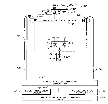
~ 35 Figure 3 illustrates a series thyristor string 32A
and its relationship to the current pulse shaping
circuitry 64 of the invention. The current pulse
shaping circuitry 64 of the invention is a dual resonant
wog6101010 ~1 q3b~6 PCr/U~9~07253 ~ .
_~_
current generator. The current pulse shaping circuitry
64 generates a first pulse current pulse train on
current loop 72A and a second half-cycle shifted current
pulse train on current 109p 72B. Each current loop
serves as a single primary turn of a current
transformer. Each current loop 72 is placed within a
dielectric tube 76, such as plastic, that runs through
the center hole of a set o~ current transformer cores 74
associated with each opposing thyristor-diode pair 36 of
lC the thyristor string 32A. (The connections to the other
opposing thyristor-diode pairs 36 of the thyristor
string 32A are omitted for the sake of simplicity).
Each current transformer core 74 has an associated
secondary winding coupled to the thyristor gate driver
70 to reduce the primary current to a rated gate current
value. The thyristor gate driver 70 combines and
rectifies the signals from the two current loops 72A and
72B to form a current pulse train firing signal for the
opposing thyristor-diode pair 36.
A few key aspects of the disclosed technology
should be noted at this time. First, a true current
source pulse stream is provided, thus variations in
thyristor impedance will not disrupt firing of the
thyristors. In addition, a shorted thyristor will not
result in serious damages to the other thyristors, as
would be the case with a voltage sourced current pulse
stream. Next, the current pulse shaping circuitry 64
operates at a low-voltage side o~ the power conditioning
device with simple isolation between the low-voltage
current pulse shaping circuitry 64 and the high-voltage
thyristor string 32A. Thus, typical bulky and expensive
transformer isolation between the power system voltage
and the gate control circuitry is obviated. Similarly,
there is no problem from electrical magnetic noise on
the power system being coupled to the low voltage
controls through a voltage pulse transformer. As a
result, the likelihood of thyristor mis-firing is
~;m;n;ch~d It should also be noted that expensive
~ WO96/0l010 2 1 ~ 3 6 ~ ~ F~ as
fiber optic equipment is not required.
Figure 4 illustrates the current pulse shaping
circuitry 64 of the invention, which includes current
pulse generating circuitry 80 and edge-triggered logic
82. Attention initially turns to the current pulse
generating circuitry 80.
Figure 5 illustrates that the current pulse
generating circuitry 80 includes a current pulse
generating circuit 80A and current pulse generating
circuit 80B. Both circuits are identical and share a
common storage capacitor C5. In current pulse
generating circuit 80A, capacitor C1 and inductor L1
comprise a resonant LC circuit. Field Effect Transistor
(FET) F1 completes the current loop for the resonant
circuit each time it is gated on. FET F3 replenishes
the charge on capacitor C1 each time transistor T1 is
switched on. Resistor R3 limits the initial current
when F3 conducts. Diode D5 shunts the base drive of T1
and prevents the charging of C1 when either F1 or its
internal diode D F1 is conducting. Diode D1 clamps the
maximum voltage of the drain terminal of F1 to the
supply voltage.
Assume that capacitor C1 is fully charged to a
positive voltage and the gate drive loop terminals are
shorted together through current loop 72A. When F1 is
gated ON, capacitor C1 discharges through Ll, the
current loop 72A, the F1 drain-source terminals and back
to the negative terminal of C1. The current flows in a
resonant manner. The activation of the gate of F1 is
shown in Figure 6(a). Figure 6(b) shows the resultant
resonant current.
Capacitor C1 then charges to a maximum negative
voltage as the LC current reaches zero as seen in Figure
6(c). The negative voltage on C1 causes the current to
~ 35 reverse direction. The current now flows through the
reverse diode D_F1, the current loop 72A, L1 and the
positive side of C1. The F1 gate drive may be removed
at any time during the negative current period and the
WO~6101010 ~' ~3~6 ,~
--10--
resonant cycle will be completed as shown in Figures
6(a) and 6(b). The voltage on Cl does not return to the
original voltage due to losses in the resonant loop,
current transformers and thyristor gate circuits. When
the resonant current becomes zero, F1 retains a blocking
state, as shown in Figure 6(d~.
To restore C1 to the original voltage value
existing before the voltage drops of the resonant loop,
the capacitor is re-charged when the resonant current is
zero. At this time, transistor Tl is gated ON. F3 is
then gated ON to provide a pulse of current to ~uickly
charge C1 to the initial voltage. This operation is
shown in Figures 6~c) and 6(e). At this point, the
circuit is ready to generate another current pulse when
F1 is gated ON in the manner previously described.
To ensure that all thyristors in the series string
conduct within a given time period, it is often
necessary to provide an initial gate pulse with a
leading edge within the given time period. Thus it is
desirable to include a steep-rise RC circuit 83 in the
current pulse generating circuitry ~0 of the invention.
The steep rise RC circuit 83A includes resistors Rll and
R13, capacitor C3 and diode D9. When F1 is gated ON,
capacitor C3 rapidly charges through resistor Rll, the
current loop 72A, transistor F1 to the negative side of
the input capacitor C5. The risetime of the current
spike is basically limited by R11 and the i~p~nce of
the current loop. This current spike is added to the
leading edge of the first current pulse generated by
each current generator circuit. Thus, the waveshape of
the first sinusoidal current pulse applied to each input
of the thyristor gate drive circuit is modified to have
a steep front edge, as shown in Figure 6(f). The first
sinusoidal current pulse from current pulse generating
circuitry 80B will have the same steep front edge.
Preferably, the steep front edge rises to a~out 0.7 amps
of secondary current in 0.5 microseconds. The disoharge
time constant (C3, R13) is set for several milliseconds
W096/010l0 ~~ q~ i3 ~ r~llL~
to ensure that only one fast rising pulse is developed
by each generator during each pulse train.
Current pulse generating circuitry 80b operates in
the same manner as current pulse generating circuitry
80a, except that the firing of F2 is shifted 180 degrees
from the firing of Fl. Thus, the positive current half
cycle of current pulse generating circuitry 80B occurs
during the negative current half cycle of current pulse
generating circuitry 80A, and vice versa. The positive
half cycle of each current loop is applied to the gate
input terminal of each thyristor in the series/parallel
string.
The currents are directed to the gate terminal by a
thyristor gate driver 70, shown in Figure 7. Note that
the unused negative half cycle currents are shorted by
diodes D3 and D4 to minimize power losses supplied by
the current generator. The shorted negative half cycle
current in one current loop is replaced by a full
positive half cycle current from the other current loop.
Thus, a train of equal positive current pulses is
applied to the thyristor gate terminal, as shown in
Figure 9(m).
The operation of the current pulse generating
circuitry 80 is controlled by edge-triggered logic 82,
shown in Figure 4. Transistor F1 of the current pulse
generating circuitry 80A is gated by a driver circuit
for a period set by a one-shot IC (monostable
multivibrator integrated circuit) 90A. Each time the
one-shot IC gOA is triggered, the Q output voltage
switches high for roughly 3/4 of the resonant period,
gating the F1 driver 92A. At the completion of the F1
drive period, the Q output switches low as the Q- output
(signal B1) goes high to enable the capacitor charge
circuit g4A.
~ 35 The capacitor charge circuit 94A is shown in Figure
8. The capacitor charging circuit quickly restores the
initial voltage level at the end of each cycle generated
by the current-source circuits. The purpose of this
WO96101010 2 ~. '? J 6 ~3 ~ ~~ Y~u,~s~ ~ .
-12-
circuit is to quickly charge the capacitor Cl to a
voltage reference level established at the positive (+)
terninal of ~ tor Ul. The voltage across Cl is
applied to the negative (-) terminal throuyh the voltage
divider of R5' and R6'. The output of Ul wlll switch to
a logic one (positive) when the reference voltage is
greater than the capacitor feedback voltage VCl. If the
NAND gate U2 is enabled by signal Bl, the output of ~2
will be logical zero and the output of U3 will be
logical one. The output of U3 thereby serves as the
base drive to transistor Tl of the current pulse
generating circuitry 80A, causing F3 to conduct and Cl
to charge to the reference voltage.
The capacitor charge circuit 94A of Figure 8
includes transistor T3 which is used to modulate the
voltage reference input to comparator Ul. That is,
transistor T3 may be turned on to reduce the voltage
reference signal to the comparator Ul when a smaller
gate pulse is desired. The base drive to T3 is signal
Dl that is developed by low current one-shot circuit 95.
When the Q output of the low current one-shot circuit 96
goes to a logical one for a selected time, T3 is
switched on and reduces the peak gate drive current
reference to Vl for that period. As a result, the
feedback signal VCl needed to switch off the Tl drive
signal is reduced and the capacitor Cl is charged to a
lower voltage. Consequently, the generated current
pulse train signal has a ~;min;~h~ amplitude.
The L- ining elements of the edge triggered logic
82 control the duration of the gate drive pulse train.
These elements include standard low cost integrated
circuits that precisely control the timer frequency,
phase shift, charging time, periods of current level
changes and the Lnitiation and duration of the current
pulse train. The oscillator 98 and the flip-flop
switcher lO0 establish the phasing between the two
current pulse generating circuits 80A and 80B. The
and Q- outputs of the flip-flop switcher lOo change
~ W096101010 2 1 '~ 3 ~ 1~ 6
state each time the clock input receives a pulse from
the oscillator 98. The oscillator 98 frequency is set
to slightly less than twice the ~C resonant frequency of
the pulse generator circuits to provide a few
microseconds of charging time for C1 and C2.
The initiation and duration of the gate drive pulse
train is established by high current one-shot circuit
102 and low current one-shot circuit 96. The high
current one-shot circuit 102 receives a gate signal from
thyristor firing command logic 62. The gate signal at
the high current one-shot circuit 102 makes the Q-
output low, thereby driving the NAND gate 104 high to
activate the input to the oscillator 9g. This initiates
a train of gate pulses. At the end of the high current
period, Q- goes high and triggers the low current one-
shot circuit 96. The Q- output of the low current one-
shot circuit 96 goes low and continues to enable the
oscillator 98. The Q output switches high, turning on
transistor T3 of the capacitor charge circuit 94A. This
changes the reference voltage to the comparator U1 low.
When the low current one-shot circuit 96 times out,
the oscillator 98 stops and the gate pulses are
terminated until the thyristor firing command logic 62
generates another pulse for high current one shot
circuit 102. During this period, the Q output of the
low current one-shot circuit 96 is zero and the
capacitor charge circuits 94A and 94B maintain the
voltage on Cl and C2 to a high value. This insures that
the first pulses of the next drive train have a high
value.
The foregoing description of the current pulse
shaping circuitry 64 of the invention is more fully
appreciated with reference to the timing diagrams of
Figure 9. The timing diagram 9(a) illustrates a start
pulse that is initiated by the thyristor firing command
logic 62. This signal drives the high current one-shot
circuitry 102 low, as shown in Figure 9(b). This action
initiates the oscillator 98, as shown in Figure 9(e) and
~0 9(i~Ul~llQ 2 1 q ~ r 8 6 ~ ~".,~
--14--
the switcher 100, as shown in Figure 9(f). In turn, the
switcher 100 initiates the one-shot IC 90A and the F1
drive 92A, as shown in Figure 91g). A half cycle later,
the switcher 100 initiates ths one-shot IC 90B and the
F2 drive 92B, as shown in Figure 9(h~.
Figure 9(i) illustrates the current spike produced
by the RC circuit 83A, while Figure 9(j~ illustrates a
half-cycle shifted current spike produced by the RC
circuit 83B. Figure 9(k) depicts the current pulse
train generated in current loop 72A, while Figure 9(1)
depicts the half-cycle shifted current pulse train
generated in current loop 72B. Figure 9(m) illustrates
the composite current pulse train firing signal. The
rectified signals of Figures 9(k) and 9(1) form the
signal of Figure 9(m). Note that the first two pulses
of the composite current pulse train gate drive signal
of Figure s(m) have steep leading edg*s (steep rises) as
a result of the current spikes shown in Figures 9(i) and
9(j)
Figure 9(m) illustrates that the amplitude of the
current pulse traln firing signal falls off after the
initial pulses. This trait i5 desirable to insure
nearly instantaneous turn-on of all thyristors followed
by a lower level of drive to reduce losses. The fall in
amplitude of the signal ~OLL~a~Cnd5 to the activation of
the low current one-shot Q output signal shown in Figure
9(d). As previously described, this signal forms a gate
drive for transistor T3 of Figure 8. The transistor
therefore turns on and pu118 down the voltag* level of
the reference voltage into the positive terminal of
comparator Ul. Thus, a reduced value of capacitor
feedback Yoltage is needed to equal the reference
voltage and switch off the T1 charge signal. This
results in a current pulse train signal with a
diminished amplitude.
The edge-triggered logic 82 of Figure 4 includes
edg*-triggered elements that are highly susceptible to
false triggering from various transients. When the
~ W096/OlOlU 2 ~ 9 3 ~ ~ 6 A ~ I /~ as
edge-triggered logic is triggered by noise it activates
that current pulse generating circuitry 80. Ultimately,
the thyristors are fired in response to a false signal.
As indicated in the background section, this can result
in the destruction of the thyristors. To avoid this
problem, the apparatus of the present invention includes
noise lock-out circuitry 66.
Figure 10 depicts the relation of the noise-lock
circuitry 66 of the invention to the other elements of
the invention. By way of overview, the noise-lock
circuitry 66 of the invention operates in the following
manner. The output of the previously described edge-
triggered logic 82 is only allowed to reach the current
pulse generating circuit 80 if the noise-lock circuitry
66 is enabled. This event occurs only if the thyristor
firing command logic 62 generates two valid signals.
The first, an edge-trigger signal used by edge-triggered
logic 82, and the second a level-trigger signal with a
duration sufficient to activate the level-triggered
logic. Since a noise spike or other transient which
would trigger the edge-triggered logic 82 is
insufficient to activate the level-triggered logic of
the invention, the edge-triggered logic 82 prevents the
noise spike or other transient from generating a pulse
stream to the series thyristor string at the wrong
instance.
The thyristor firing command logic 62 generates a
signal on the edge-triggered logic line 106 of the edge-
triggered logic 64 and a signal on the noise lock-out
line 108 of the noise lock-out circuitry 66. Typically,
the thyristor firing command logic 62 will be in the
form of a microprocessor executing appropriate software.
The software will generate thyristor firing ~o~~-n~q
based upon a control strategy, such as only firing the
thyristors when the line voltage is within 10% of the
compensating capacitor voltage, a zero voltage crossing
scheme, or the like. In any event, the noise lock-out
circuitry 66 includes level-triggered logic 110. The
wog6~~ 0 ~ ' ~ 3 6 ~ ~ r~ u..,!,. ~
level triggered logic 110 is not activated by an edge,
rather it is only activated by a sustained signal and
only operates during the duration of the signal.
Therefore, a noise spike or other typical transient
would not activate the level triggered logic 110. The
level-triggered logic 110 may be implemented as serial
inverters. The serial inverters also serve to boost the
computer signal sufficiently to drive a switch.
When a valid activation command is generated by the
thyristor firing command logic 62, the level-triggered
logic 110 generates an output signal on line 111 which
is used to close switch 112. Preferably, the signal on
line 111 is boosted with a driver 113 to provide a
boosted signal on line 115. When switch 112 is closed,
the drive power for the current pulse generating circuit
80 is present, thus allowing the current pulse
generating circuitry 80 to produce its output on 72A and
72B for the thyristor gate drives 70.
The noise lock-out circuitry 66 of the invention
optionally includes a Schmitt Trigger 116 with a low-
pass filter. The low-pass filter may be implemented as
an RC circuit with a time constant set in accordance
with the largest expected noise pulse width.
Figure 11 illustrates an ~mho~ nt of the level-
triggered logic 110 of the invention. In thisembodiment, an active low signal from the thyristor
firing command logic 62 is applied to level-triggered
logic line 108. Since the computer signal is not
suitable for driving a FET directly, an inverting
peripheral driver integrated circuit is used comprising
inverters 130 and 132. The output of the inverters of
the level-triggered logic is used to turn-on the actlve
low gate of lock-out FET LO. FET LO enables the drive
power to the current pulse generating circuit 80. lf
this drive power is not present, then the open collector
outputs the edge-triggered logic 82 cannot be pulled up
to a level sufficient to drive switch 112 into the on
state. Thus, in this embodiment of the invention,
~ WO~6101010 21 936~3~ r~ s~ .
-17-
switch 112 is implemented as FET LO, which initiates
operation of the current pulse train.
Thus, it will be appreciated that the present
invention describes a thyristor gate drive device that
provides uniform gate current pulses, regardless of
variations in thyristor im~e~nr~ or the presence of
failed thyristors. The invention also provides a
thyristor gate drive device that operates at low voltage
and thereby eliminates the requirement for costly and
complicated high-voltage side control devices.
Furthermore, the low voltage-side thyristor gate drive
circuitry of the invention i5 isolated from the high-
voltage side of the device with a simple and in~Yr~nqive
isolation r-~h~n;-m The disclosed invention also
provides a technique for eliminating the problem of
false thyristor gate firing signals.
The foregoing descriptions of specific embodiments
of the present invention are presented for purposes of
illustration and description. They are not intended to
be exhaustive or to limit the invention to the precise
forms disclosed, obviously many modifications and
variations are possible in view of the above t~~h;ngs.
The Pmho~; r-ntS were chosen and described in order to
best explain the principles of the invention and its
practical applications, to thereby enable others skilled
in the art to best utilize the invention and various
embodiments with various modifications as are suited to
the particular use contemplated. It is intended that
the scope of the invention be defined by the following
Claims and their equivalents.