Note: Descriptions are shown in the official language in which they were submitted.
~ WO 96139780~ 2 1 9 4 3 8 3 PCT/US96l07980
RADIO ~ u~ _ I TR~ K
HAVING ~w~ ~ MODE POWER SUPPLY
BA~KUUN~ OF THE lNV~
.
The invention relates in general to radio
frequency transmitters and, in particular, to a switched
mode power supply for a radio frequency transmitter.
Garage door opPrPtnrs commonly may be controlled
from wired switches as well as radio frequency transmittins
switches such as hand-held radio transmitters. Hand-held
radio transmitters are energized by a battery and it i5
desirable to ~-~nt~n as long a battery life as posaible.
However, it is also important for hand-held radio trans-
mitters to be inPYrPnqive~ while still conforming with
requirements of the Federal ~ ;r~t~nnq C ~sion for
center frequencies, bandwidth limitations, power limi-
tations and the like. In the past hand-held radio trans-
mitters, particl~lArly of the type disclosed in U.S. Patent
No. 4,806,930 to Wojciak, Jr., were directed to battery
operated systems wherein a radio transmitter might include
a code gPnPratnr as well as an osc~ tor having an output
' l~ted in some fashion by a code gPnPrator for producing
a - l~tP~ radio frequency output. The transmitter was
energized by a battery E.
Such a transmitter, however, was relatively
hulky, in part because relatively large batteries, such as
9-volt and 12-volt batteries were used to energize the
tr~n~tters. Today, however, people have come to enjoy
keyfob-type transmitters which have very small volumes and,
accordingly, in many cases are now using 3-volt lithium
batteries. Unfortunately, 3-volt lithium batteries do
suffer from voltage drop off with battery life and the
initial voltage of the batteries as received from the
supplier varies to some extent. As a result, the trans-
mitter radio frequency gPnPrat~ng section will not always
receive the same energizing voltage and this may lead to
the transmitter drifting in frequency and possibly having
.~ 3 :.
WO96/39780 t~ P~ T~ ~9g383 Pcr/US96107980 ~
-- 2 --
its electrical ~h~rPctPristics DffectDd greatly by the
change in the battery voltage that it will be unable to
osr~ te at all and, hence, will be unable to gDnPr~te a
radio frequency signal.
What is needed, then, i8 a hand-held radio
fre~Pncy transmitter ~nr~ ng a voltage st~hil~7D~ power
supply which is compact and has a relatively small number
of cn~nnDnt~.
SUMWARY OF T~E lNV~N'l'lU
~0 A hand-held radio freguency transmitter includes
a switch mode power supply for delivering a pre-selected
potential to a radio-frequency os~ tor. The 6witched
mode supply is controlled by a micLu~LucessuL or other
digital logic device, such as an application-specific inte-
grated circuit or a custom ~ntegrate~ circuit and ;nr1uAPR
a switch controlled by the mi~Lu~LucegsoL, which switch
enables or ~lD~hlpR current from flowing through an induc-
tor coupled to a storage c~p~c{tor. A feedback loop i8
coupled to the storage capacitor for signalling the micro-
controller when the storage ~p~r;tnr has reached a pre-
selected voltage. A radio frequency os~ tor is
cnnnected to be energized from the 8torage capacitor and
~ludPR an input for receiving a -' lAt~ng code. The
~ t;ng code causes the o~r~ tor to be switched on and
off, thereby producing a pulsed carrier wave which may be
supplied to a garage door orPr~tor or other device to be
opPr~ted.
It is a principal aspect of the preEent invention
to provide a hand-held radio frequency transmitter
30 ~n~lu~lng a switch mode power supply driven from a battery
for supplying unlform potential electrical energy to a
radio frequency osc;11~tor.
Cther advantages o~ the present invention will
become apparent to one of ordinary skill in the art, upon
~ $ ~
Wos6~9780 ~ ~ ~ Q ,~ S 2 1 9 4 3 8 3 P~
a perusal of the following sper~flr~t~n~ and claims in
light of the a~ , ylng drawings.
BRIEF DESCRIPTION OF THB D~ ~TNr,~
PIG. 1 is a 8~h~ t~c diagram of a hand-held
radio fL~uen~y transmitter embodying the present inven-
tion; and
FIG. 2 is a flow chart ~howing operation of a
microcontroller of the radio frequency transmitter shown in
FIG. 1.
DETAILED DESCRIPTION OF T~E ~K~Kh~ EMBODIMENT
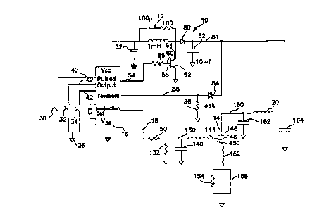
Referring now the drawings and P~per~lly to FIG.
1, a hand-held radio frequency transmitter embodying the
present invention is ge~er~lly shown therein and is iden-
tified by numeral 10. m e transmitter 10 inr~ a switch
mode power supply 12 coupled to a radio frequency oscllla-
tor 14. A microcontroller 16 produces a '~t~ng code on
an output line 18 which is supplied to the 08~11 ator 14
for causing the osc~ tor 14 to generate radio frequency
energy which is emitted by an antenna 20 and which may be
received by a garage door op~r~tor or other device to be
operated.
A plurality of switches, respectively ~umbered
30, 32 and 34, are cnnn~cted in p~rallel to a ground 36 and
to ~hree inputs 40, 42 and 44 of the microcontroller 16.
Closure of switches 30, 32 or 34 each will respectively
cause a different m~ tlon code stream to be produced by
the microcontroller 16 on the line 18. For instance, each
of the switches may be dedicated to a particular garage
door 80 that three garage doors could be op~rated separate-
ly from the three switche3. In the ~lt~rn~t~ve, one of the
switches might be de~c~ted to sending the code, which
would cause a light to be il~ 'n~te~ within the garage
W09639780 ~ S ~ 1 94383 PCT~S960~98
even when a garage door i8 not being opDn~P~i. In response
to closure of one of the three switcheg 30, 32 and 34, the
modulation output is s~pplied on line 18 to a resistor 50
which ultimately feeds to the osci~l~tnr 14. The oscilla-
tor 14, however, must be energized in order to provide anoutput. It ~hould be appreciated that a battery 52 i9
coupled to VCC pin of the microcontroller 16 to energize it
at all time8. The mi~Lucu..tLùller 16 may, for instance, be
a CMOS 8-bit microcontroller such as a Zilog Z86C03. One
of the pins of the mi~Locu~Lroller 16 provides a pulsed
output at pin 54 which is fed through a 470-ohm resistor 56
to an NPN transistor 58 which receive~ the pulses at its
base 60, transistor emitter 62 is connocte~ to ground and
its cnllector 64. Current from the battery 52 may be
supplied to a one mi 11; h~nry in~nctnr 70 coupled to the
battery 52 and to the collector 64. A pulse on the line 54
switches the transistor 58 of ~ llnrollrl ing the inri~lctor 70
from ground and causing current to flow through a diode 80
to a 10 microfarad electrolytic capacitor 82 and charging
the 10 microfarad electrolytic capacitor 82 until the point
that it reaches a voltage which is e~ual to the breakdown
voltaye of a Zener dlode 84 cnn"Pcte~ to the capacitor 82.
A 100 kilohm resistor 86 is cn"nPcted between the Zener
diode 84 and ground and a feedback line 88 couples the
junction of the Zener diode 84 and resistor 86 to a feed-
back input tPrmi"~l on the mi~LucuntLuller. Thus, when the
Zener diode goes into avalanche, driving the line 88 high,
the microcontroller drives the pul8ed output 54 high, bia~-
ing the transistor 58 on and interrupting current flow to
the capacitor 82. The capacitor 82, however, has received
sufficient potential to energize the osrillAtor 14 as will
be ~een hereinafter.
Referring now to FIG. 2, operAtinn of the micro-
controller 16 is 8hown therein. In a step 100 an interrupt
occurs every 50 milliseconds. In a step 102, a test is
made to ~tPrm;nP whether the pul8ed output pin cn"nected
~ W096~9780 ~,~gf~ T5 2 1 9 4 3 8 3 PcT~s96lo798o
to the line 54 is high. If it 18 high, the switched mode
output on the line 54 is set low in a step 104. If the
test of step 102 is negative, a test is made in a step 106
to determine whether the fPeAhar~ input on line 88 is high.
~ 5 If it is, control is transferred to the step 104, causing
the pin crnnPrtP~ to line 54 to switch low. If it is not,
control is transferred to a step 110, cauging the switch
mode output line ronnPcteA to line 54 to switch high, turn-
ing on transistor 58. In a step 112, a test i8 made to
determine whether the period for the , 17tir~n bit timing
for the lAt1On generated on line 18 has expired. If
the period for lP~on bit timing has expired, the
routine i8 exited in a step 114. If it has not expired,
the next bit position i8 nht~lnpA in a step 116 and it is
outputted, following which the routine i8 exited in a step
118.
The l~rirn bit8 8l~rpliPA to resistor 50 are
fed to a line 130 after having been reduced in potential by
the voltage divider, ~nr~llA~nrJ resistor 50 and a resistor
132, cnnnPcted thereto. A capacitor 140, connected to
ground, compriseR a s~hil~;ng filter capacitor and is
connected to a series ~rAllctor 142 which blocks radiation
of stray harmonics of the radio frequency in the range of
300 to 400 MHz. The l~teA signal is then fed to a base
144 of an NPN transistor 146, also having a collector 146
and an emitter 150. The emitter 150 is CnnnPctPA through
an inductor 152 for h~ ~ ~R ~uy~L~s~lon and through a
parallel resistor 154 and capacitor 156. The resistor 154
and capacitor 156 which are crnnPctPd to ground. The
resistor 154 sl~rp1ieR control over the DC bias and the
capacitor 156 controls the radio frequency gain of the
oscillator of transistor 146. The emitter 148 of the
transistor is cnnnPcted via a line 160 to a grounded
capacitor 162, having an antenna coil cnnnPrteA thereto.
A second grounded capacitor 164 is connected to the line 81
as well as to the antenna coil 20. The coded tL - Rsion
W096~9780 ~ 9 4 3~ 3 PCT~S9610~980
-- 6 --
is transmitted by the antenna 20 to a garage door operator
or other device to be operated as appropriate. Attached a3
Appendix A is a listing of ,- ,_8~r instructions used in
implementing the present ~
While there have been illustrated and described
particular ~ s of the present invention, it will be
appreciated that numerous changes and modifications will
occur to those skilled in the art, and it is lntPn~d in
the appended claims to cover all those changes and modifi-
cations which fall within the true spirit and scope of the
present invention.
~ W0 96/39780 ~ 'pi~ 7 2 ~ 9 4 3 8 3 PCTIUS96107980
APPENDIX A
EQUATE STATEMENTS
P01 M_INIT .EOU 00000100B ; set mode p00-p03 out
P2M INIT .EQU 00000001 B
P3M_INIT .EOU 00000001 B ; set port3 p30-p33 hput
P01S iNlT .EQU 00000001B
P2S_INIT .EOU 00000000B
P3S_INIT .EOU ooooooooB
INTERRUPTS
ALL_ON_IMIR .equ 00010000b ;tumon intforradio
RETURN_IMR .equ 00010000b ; retum on Uhe IMR
;
GLO8AL HtGi;:i I tHS
;
Code output functions
.. . . .. . . . . . .. .... .
CODE GRP .eqL 10H
CODEPOS .ffU CO9 GRP+0 ;codepresenUybeingoutputed
C11 .ec u CO ~~ GRP+1 ; code first bit
C12 .ecu CO~ GRP+2 ;codesecondblt
C13 .er u CO ~ C ~P+3 ; code third bit
C14 .ecu CO~ G~P+4 ;codetourlhbit
C15 .ec u CO ~ G ~ '+5 ; code fifth bit
C16 .ecu CO~ G~'+6 ;cocesixedbit
C17 .ec u CO ~ G ~ '+7 ; coc e seventh bit
C18 .ec u CO ~ G '~ '+8 ; coc,e eight bit
C19 .ec u CO ~ C ~ '+9 ; cooe nineth bit
C110 .ec u CO ~ G ~ '+10 ; coce tenth bit
TEMP .ecu CO ~ G ~ '+14 ; temp nurnber for finding acdress
BITTEMP .ec u CO ~ _G ~ '+15 ; the bit value temp
codepos .eou rO
c11 .ec u r1
c12 .ecu r2
c13 .ecu r3
c14 .ecu r4
c15 .ecu r5
c16 .ecu r6
c17 .ecu r7
c18 .ecu r8
c19 .ecu r9
c110 .ec u r10
temp .ecu r14
bittemp .ecu r15
W096139780 ~ t~ 943~3 PCr/USs6/07980
, Codeoutputfunctions . .. .....
CODE2_GRP .eqc 2~H
C21 .ecu CO ~ 2_GR '+1 ; code fird bit
C22 .ecu CO~ 2 GR'+2 ;codesecondbit
C23 .ecu CO~ 2 G~'+3 ;rodethirdbit
C24 .ec u CO ~ 2_G ~ '+4 ; r ode tourth bit
C25 .er u CO ~ _ G ~ '+6 ; code tif~h bit
C26 .ec u CO ~ 2_G ~ '+6 ; code sixed bit
C27 .ec u CO ~ 2 G ~ '+7 ; code seventh bit
C28 .ecu CO ~ __C ~ '+8 ; code ei~ht bit
C29 .ecu CO~ '_GRP+9 ;codeninethbit
C210 .ecu CO~ F_GRP+10 ;codetenthbit
c21 .ec u r1
c22 .ec u r2
c23 .ecu T3
c24 .ecu r4
c25 .ec u r5
c26 .ecu r6
c27 .ec u r7
c28 .ec u r8
c29 .ecu r9
c210 .ecu r10
CHECK GRP .equ 30H
CODECNT .equ CHECK_GRP ; / DOWN FOR 1 mS
STACKTOP .equ 127D ; dart ot the stack
STACKEND .equ 060H ; end ot the stack
WDT .macro
.byte 5th
.endm
WDH .macro
.byte 4th
.endm
FILL .macro
.byte OFFH
.endm
TFLL .macro
FILL
-ILL
-ILL
-ILL
-ILL
=ILL
ILL
FILL
FILL
FILL
WO 96139780 , ~ 2 1 9 4 3 8 3 PCrlUS96/07980
~ _ g _
.endm
HFILL .macro
TFILL
TFli L
TFli L
i L
LL
L
LL
LL
--I LL
.endm
... ..... . . .
;'
~ ;- interrupt Vector Table
.... ...... .
.org 0000H
.word 000CH ;iRQ0 '3.2 n
.word 000CH ;IRQ1, '3.3
.wond OOOCH ;IRQ2, '''.1
.word 000CH ;IRQ3, '0.2p
.word TIMERUD ;IRQ4, T0
.word 000CH ;IRQ5, T1
.org 000CH
, WATCHDOt~ INiT!LlZATlON
;-
start:
START: di ; tum otl the intemupt for init
WDH
WDT ; kick the dog
, STACK INITILIZATION
. ... .. . .. ...
SETSTACK:
dr 254
Id 255,#STACKTOP ; sel the start of the stack
, DATA INITILIZATlON ... .
PIT1 TO10
Id C11,N03 ; code 3~.~3.~ 33.~ MAX POWER
Id C12,#03
Id C13,#03
Id C14,#03
W096/39780 ., ~ 3 PCrlUS96/07980 ~
-- 10 --
d C15,#03
d C16,#03
d C17,#03
d C18,#03
d C19,#03
d C110,1~03
BIT11 TO20
c C21,#03; c ode ~3 ~ 3 ~ 333 MAX POWER
c C 23,#03
c C24,#03
c C25,#0.,
d C26,#09
d C27,#03
Id C28,#03
Id C29,#03
Id C210,#03
dr CODEPOS
, TIMER INITILIZATION
Id PRE0,#00000101B ;setthepresralertol1 for4Mhzxtsl
Id PRE1,#01000010B ; one shot mode n 6
Id To,#o~H ; set Ule counter to ccunt ~ through 0
Id TMR,#00000011 a ; tum on the limer
. . .
; PORT INITILIZATION
Id ~o~#pn1 S_INIT ; RESET all pOlts
Id '2,#P7S_INIT
Id '3,#P'S INIT
Id '01 M,ilP01 M_INIT ; set mode
Id '3M,#'3M_INIT ; set port3 p3~p33 input snalo~ mode
Id '2M,#'2M_INIT ; set port 2 mode
.... . .. .. .
; INITERRUPT INITILIZATION
.
SETINTERRUPTS:
Id IPR,#00000û0113 ; set the priority to timer
Id IMR,#ALL_ON_IMR ; tum on fhe interrupt
.. . . .... ... ...
; MAIN LOOP
MAINLOOP
ei ; enable intemupt
Id P01 M,#P01 M_INIT ; set mode
-
Wo 96139780 .l ~- ~, P ~ ll 2 1 ~ 4 3 8 3 PCIIUS96/07980
Id P3M,#P3M INiT ; set pori3
Id P2M,#P2M INiT ; set port 2
jr MAINLOOP
.
. .
; TIMER UPDATE FROM INTERUPT EVERY 50uS
;.
TIMERUD:
WDT ; kick the d~
-m P2,Jt0000000t b ; test for the voitage max meet
r z,dearexa
~or P2,#000û0010b ; toggle the output pln
r CODE
clearexa:
and P2,#11111101 b ; tum off the output
CODE:
dec CODECNT ; decrease the code counter
jr nz,NOCODFOUT
Id CODECNT,#20d ; set the count tor 1 mS period
ei ; ailow stacking of intemupts
call CODEOUT ; ouiput the code
N-OC(:IDFOUT:
iret
, CODE OUTPUT ROUTINE EVERY 1 mS
. .
CODEOUT:
BILLOUT
inc CODEPOS ; set the position to the next one
cp CODEPOS,#1 60d ; tust br the last count position
jr ult,ACODEOP ; if not the last count then conbnue
cir CODEPOS ; else reset the counter
ACODEOP:
cp CODEPOS,#128D ; test for the blank time
jr uit,ABL2 ; if not the do the code
jp OFFEXiT ; tum off the output
~BL2:
cp CODEPOS,#83D ; test tor second frame active 0me
jr ugt,AF2 ; U the second frame then jump
cp CODEPOS,J~44çi ; test br the first blank time
jr uit,ABL3 ; a not the first blank time then output
bits
jp OFFi-XlT ; blank tiem tum off the outputs
ABL3:
cp CODEPOS,N03 ; tegt for the sync
jr ugt,ABiTS ; H not do the bits
jp z,ONEXlT ; U sync time set the output
jp OFFEXIT ; else turn off the output
ABiT5
Id TEMP,CODEPOS ; get the present counter
rct ; dear the cany flag
nc TEMP ;/2
rct ; dear the cany flag
Wo 96/39780
rrc --'Jl ' ; /4
aod ~~' ',#CODE_GRP ; add in the off aet
Id , ~ MP,@TEMP ; read ths bit to output
Id ~ ',CODEPOS ; ~et the psit on in the bit
end ~ M',~0000011B
sod ~ U ', llTTEMP ; see it the output neerJs to be set
cp ~ H ',1 ~~ ;
jr u,o~F~xlT
;p o~ r
AF2:
Id TEMP,CODEPOS ; remove the ofl set
sub TEMP,~iô4D
cp TEMP,#03 ; test for the sync
jr ugt,ABlTS2 ; it not do the bits
cp TEMP,N00
jp ugt,ONEXlT ; it sync tirne set the output
jp OFFEXIT ; else turn off the output
ABITS2:
rcf ; dear the carry flag
rrc TEMP ; / 2
ncf ; dusr the carry flap
nc ~ M' ;/4
add ~ M ',#CODE2_GRP ; add in the ofl set
Id I -r ~J p,@TEMP ; read the bit to output
Id M ',CODEPOS ; Set the position in the bit
and ~ M',=00000011B
add T M ', llTTEMP ; see il the output needs to be set
cp ~ M',~104
jr u ,O-FEXIT
jp ONEi(lT
ONEXIT:
Id P0,#~0 I L, ; tum on the output
jr CODEDONE
OFFEXIT:
Id P0,#0000001 OB ; tum off the output
CODEDONE:
ret
.end