Note: Descriptions are shown in the official language in which they were submitted.
WO96/01502 2 1 9 4 4 0 0 PCT~S~5~ 5~
-
DESCRIPTION
EPITAXIAL THALLIUM HIGH TEMPERATURE SUPERCONDUCTING
FILMS FORMED VIA A NUCLEATION LAYER
Field of the Invention
The present invention relates to epitaxial high
temperature superconductor thin films on substrates
preferably having low (e.g. less than 30) and isotropic
dielectric constants, and a low dielectric loss tangent
(e.g. less than 10-4) particularly epitaxial high tem-
perature superconductor thin films for use in microwave
and/or RF applications. For example, the present inven-
tion relates to epitaxial thallium and copper oxide
based superconducting thin films, such as TBCCO, on MgO.
Federal Funds Statement
Federal funds from Strategic Defense Initia-
tive/Innovative Science and Technology under Contract
No. N00014-92-C-2155 were used in the reduction to prac-
tice of the invention.
Backqround
There are many benefits to including superconductive
elements in electronic circuitry. Superconductivity re-
fers to that state of metals and alloys in which the
electrical resistivity is zero when the specimen is
cooled to a sufficiently low temperature. The tempera-
ture at which a specimen undergoes a transition from a
state of normal electrical resistivity to a state of
superconductivity is known as the critical temperature
(Tc). The use of superconductive material in circuits is
advantageous because of the elimination of normal elec-
trical resistive losses.
In the past, attaining the Tc of known superconduct-
ing materials required the use of liquid helium and
expensive cooling equipment. In 1986 a superconducting
material having a Tc of 30 K was announced. See, e.g.,
Bednorz and Muller, Possible High Tc Superconductivity
WO96/01502 PCT~S95/09063
21 94400
in the Ba-La-Cu-O System, 64 Z.Phys. B-Condensed Matter
189 (1986). Since that announcement superconducting
materials having higher critical temperatures have been
discovered. Collectively these are referred to as high
temperature superconductors (HTSs). Currently, HTSs
having critical temperatures in excess of the boiling
point of liquid nitrogen, 77 K (i.e. about -196 ~C or
about -321 ~F) at atmospheric pressure, have been dis-
closed.
Superconducting compounds consisting of combinations
of alkaline earth metals and rare earth metals such as
barium and yttrium in conjunction with copper (known as
"YBCO superconductors") were found to exhibit supercon-
ductivity at temperatures above 77 K. See, e.g., Wu, et
al., Superconductivity at 93 K in a New Mixed-Phase Y-
Ba-Cu-O Compound System at Ambient Pressure, 58 Phys.
Rev. Lett. 908 (1987). In addition, high temperature
superconducting compounds containing bismuth have been
disclosed. See, e.g., Maeda, A New High-Tc Oxide Super-
conductor Without a Rare Earth Element, 37 J. App. Phys.L209 (1988); and Chu, et al., Superconductivity up to
114 K in the Bi-Al-Ca-Br-Cu-O Compound System Without
Rare Earth Elements, 60 Phys. Rev. Lett. 941 (1988).
Furthermore, superconducting compounds containing thal-
lium have been discovered to have critical temperaturesranging from 90 K to 123 K (some of the highest critical
temperatures to date). See, e.g., Koren, et al., 54
Appl. Phys. Lett. 1920 (1989).
These HTSs have been prepared in a number of forms.
The earliest forms were preparation of bulk materials,
which were sufficient to determine the existence of the
superconducting state and phases. More recently, HTS
thin films on various substrates have been prepared
which have proved to be useful for making practical
superconducting devices.
It is desirable to use HTS films for microwave and
-RF applications. Optimally, such HTS films must have
' WO96/01502 2 1 9 4 4 0 0 ~CT/U~5S~ '3
_
low surface resistance and must be able to handle sig- -
nificant power levels. It is preferred that HTS films
used for microwave applications have a high Tc and have a
substantially linear response at high power levels (i.e.
R8 does not significantly vary with RF current density).
Many of these criteria are satisfied by HTS films which
have both a low fault density and are epitaxial. Epi-
taxy refers to that state of a film wherein there is a
systematic and single (or uniform) orientation of the
crystal lattice of the film with respect to the sub-
strate. However, not many films exhibit linear perfor-
mance characteristics.
Epitaxy may even be necessary for certain HTS films
to exhibit desirable microwave and RF applications prop-
erties. For example, epitaxial TBCCO thin films (i.e.films containing thallium, barium, optionally calcium,
and copper oxide) exhibit desirable microwave proper-
ties. See Eddy, et al., "Surface Resistance Studies of
Laser Deposited Superconducting Tl2Ba2CalCu2O~ Films," 70
J. Appl. Phys. 496 (1991). Examples of various phases
of such TBCCO thin films which are known to exist in-
clude Tl2Ca1Ba2Cu2O8 (i.e. 2122), Tl2Ca2Ba2Cu3Ol0 (i.e.
2223), TllCalBa2Cu2O, (i.e. 1122), and TllCa2Ba2Cu3Og (i.e.
1223). See Olson, et al., "Preparation of Supercon-
ducting Tl-Ca-Ba-Cu Thin Films by Chemical Deposition,"
55(2) Appl. Phys. Lett. 188 (1989); and Beyers, et al.,
"Crystallography and Microstructure of Tl-Ca-Ba-Cu-O
Superconducting Oxides," 53(5) Appl. Phys. Lett. 432
(1988). However, TBCCO thin films having optimal or
uniform nucleation grow on only a few substrates (e.g.
such TBCCO thin films have been shown to grow on LaAlO3
and SrTiO3).
In addition, LaAlO3 is the only substrate at present
upon which TBCCO films suitable for microwave applica-
tions may be grown, but such films exhibit non-linear
performance characteristics. Also disadvantageously,
LaAlO3 substrate exhibits a high dielectric constant
WO96/01502 PCT~S95/09063
21 94400
which is variable due to twinning. These properties of
LaAlO3 make microwave design difficult. For example,
microwave design and microwave performance modelling is
limited by the use of LaAlO3 as a substrate. The high
dielectric constant results in line widths at high fre-
quencies which are narrow, and excessive twinning limits
frequency setability to +/- 1 percent.
Important microwave and RF applications require
twin-free, low dielectric constant substrates. In addi-
tion, it is preferred that the substrates be availablein large areas (two inch round or greater) to fabricate
devices such as narrow band filters at desired frequen-
cies. Substrates such as MgO satisfy these criteria.
However, good HTS thin films which are thallium and
copper oxide based, such as TBCCO, do not easily grow
epitaxially on MgO. Often, such HTS films grow on MgO
in several orientations, resulting in high angle grain
boundaries and degraded superconducting properties.
The prior art has failed to provide a combination of
both a good HTS film and a good substrate which exhibit
properties suitable for microwave and/or RF applica-
tions. Specifically, the prior art does not provide a
device suitable for such applications comprising a HTS
film having low surface resistance, exhibiting substan-
tially linear response characteristics at high RF cur-
rent density (i.e. R8 does not significantly vary with RF
current density), and which can be grown on a substrate
which has a low dielectric constant, which is twin-free,
and which does not degrade the superconducting proper-
ties of the film.
SummarY of the Invention
The present invention comprises a high temperaturesuperconducting (HTS) film on a substrate (and a method
of providing the same) wherein the HTS film and sub-
strate combination exhibits properties s~itable formicrowave and/or RF appli-cations. Specifically, the
WO96/01502 2 1 9 4 4 00
-
present invention provides a device suitable for micro- -
wave and/or RF applications comprising HTS films having
low surface resistance, exhibiting linear response char-
acteristics at high RF current density (i.e. R8 does not
significantly vary with RF current density), and which
can be grown on a substrate which has a low dielectric
constant, which is twin-free, and which does not degrade
the superconducting properties of the film. The present
invention also comprises a method of providing the same.
10The present invention comprises a high quality,
epitaxial HTS thin film which is thallium and copper
oxide based, such as TBCCO, on both MgO and other sub-
strates and a method of providing the same. It is pre-
ferred that a thallium based HTS film be used because
such films exhibit Tcs which are higher than other films.
The present invention is achieved using a nucleation
layer to provide a template for subsequent HTS film
growth. Broadly, a two-step process consists of first,
forming ln situ an intermediate layer of YBCO (or a
structural analog) on a support layer, and second form-
ing a thallium and copper oxide based film on the inter-
mediate layer by precursor deposition followed by a
post-deposition thermal processing for crystallization.
In this way the benefits of high quality in situ crystal
growth are combined with the predictable thallium HTS
manufacturing techniques to form a high-quality thallium
HTS film. More specifically, a YBCO film or a film hav-
ing growth characteristics (e.g. can be grown in situ)
and physical structures (e.g. lattice structures in the
a-b plane) analogous to YBCO films (i.e. a YBCO analog)
is used as a nucleation layer on MgO or another sub-
strate to enable the growth of epitaxial HTS films such
as TBCCO. Although YBCO may form an HTS film itself, it
is not necessary that the nucleation layer be an HTS or
a superconducting film. For example, YBCO could be used
or a bismuth film could be used in place of YBCO. Bis-
muth films qualify as YBCO analogs as bismuth films and
WO96/01502 PCT~S~
21 94400
YBCO films both can be grown ln situ epitaxially and
both have analogous a-b plane lattice structures. Addi-
tional examples of films which can be used as a nucle-
ation layer (i.e. films which qualify as YBCO analogs)
include bismuth cuprates, neodymium cerium cuprates,
lanth~nllm cuprates, and strontium cuprates. Doping or
substitutions in such films may be used. For example,
praseodymium or other rare earth may be substituted for
the yttrium in the YBCO to make an acceptable non-super-
conducting nucleation film.
In the preferred embodiment, YBCO is used as a nu-
cleation layer between MgO and TBCCO. In situ growth of
YBCO occurs in a single, epitaxial orientation on MgO.
Using such a layer of YBCO as a nucleation layer for
TBCCO allows the orientation information to pass between
the two layers. In addition, using a thin layer of YBCO
as a nucleation layer allows the passage of orientation
information without degradation of the top TBCCO layer
due to interdiffusion between YBCO and TBCCO. With a
thin YBCO layer there is not sufficient interdiffusion
to significantly degrade the superconducting properties
of the TBCCO layer. Preferably, the YBCO layer is be-
tween about 10-600 A in thickness as the layer should be
thick enough to be pin-hole free and the unit cell
thickness of YBCO is approximately 10 A.
The preferred method of preparing a MgO substrate is
by in situ growth of a thin YBCO or YBCO analog film
layer on the substrate. This same method could be used
to prepare a different substrate buffered by YBCO or a
YBCO analog film. A high vacuum system may be used for
the in situ growth of YBCO (or YBCO analog) which may be
deposited by laser ablation, sputtering, CVD (chemical
vapor deposition), MBE (molecular beam epitaxy), or
other deposition methods.
The preferred method of growing a TBCCO film on the
thin YBCO (or YBCO analog) layer is to first deposit a
precursor layer by laser ablation, sputtering, CVD, MBE
WO96/01502 PCT~S95/09063
_ 21 94400
or other deposition method. The precursor layer is then
crystallized, preferably by annealing at high tempera-
ture in a reactor which controls the thallium loss dur-
ing the post-deposition processing. This method is
known as the Epitaxial Lowloss Film or ELF method and is
described in detail in Olson et al., U.S. Pat. No.
5,071,830, and Eddy et al., U.S. Pat. No. 5,139,998,
both of which are assigned to the applicants' assignee.
As is mentioned above, thallium films are preferred
because they achieve high Tcs.
Additional layers may be grown on the MgO or other
substrate before deposition of the YBCO or YBCO analog
layer. Having such additional layers allows progressive
grading of any lattice mismatch between the substrate
and the YBCO or YBCO analog (e.g. the lattice mismatch
between YBCO and MgO is about 10%). By grading the
lattice mismatch, there is a lesser likelihood of expe-
riencing grain boundary rotations (i.e. lesser likeli-
hood of seeing grains lying parallel to the growth sur-
face but which are not aligned) and, therefore, a betternucleation layer is provided. Examples of acceptable
grading layers include barium titanate (BaTiO3), stron-
tium titanate (SrTiO3), barium zirconate (BaZrO3), and
calcium zirconate (CaZrO3) among others. Such grading
layers are well known by those skilled in the art.
In addition, it is well known by those skilled in
the art that certain substrates require buffer layers to
limit interdiffusion between the substrate and any over-
lying layer. Such buffer layers may be provided on
substrates used in the present invention.
The growth of epitaxial HTS thin films which are
thallium and copper oxide based, such as TBCCO, on large
area substrates which have low dielectric constants
enables the production of HTS devices which are useful
for microwave and/or RF applications.
WO96/01502 PCT~S95/09063
21 94400
It is a principal object of the present invention to
provide a thallium based HTS film which is suitable for
microwave and/or RF applications.
It is also on object of the present invention to
provide a thallium based HTS film on a substrate which
is suitable for microwave and/or RF applications.
It is an additional object of the present invention
to provide an epitaxial thallium based HTS film on a
substrate which is suitable for microwave and/or RF
applications.
It is a further object of the present invention to
provide a thallium based HTS film on a magnesium oxide
substrate.
It is another object of the present invention to
provide a thallium based HTS film on a magnesium oxide
substrate using as a nucleation layer a thin film which
has growth characteristics and physical structures anal-
ogous to a yttrium based thin film.
It is yet another object of the present invention to
provide a thallium based HTS film on a magnesium oxide
substrate using as a nucleation layer a yttrium based or
bismuth based thin film.
It is still another object of the present invention
to determine and define growth conditions which are
compatible for growth of the thallium based HTS films
set forth above.
It is yet an additional object of the present inven-
tion to provide an HTS film which exhibits a linear
response up to high RF current densities.
Brief Description of the Drawings
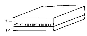
Figure lA is a cross sectional view of a substrate
having a YBCO or YBCO analog thin film as a nucleation
layer and a thallium based precursor layer.
Figure lB shows a cross sectional view of the device
of Figure lA after post-deposition thermal processing
- has crystallized the precursor layer.
WO96/01502 PCT~S95/09063
2 1 ~440û
Figure 2 shows the microwave performance of TBCCO
films on MgO with a YBCO nucleation layer compared to
the microwave performance of a TBCCO film on LaAlO3.
Figure 3 shows the critical temperatures of TBCCO
films on various substrates.
Detailed Descri~tion of the Preferred Embodiment
A high quality, epitaxial high temperature supercon-
ducting (HTS) thin film containing thallium and copper
oxide can be provided on MgO and other substrates. Such
substrates preferably have characteristics favorable to
microwave and/or RF applications. Using nucleation
layers which provide a template for subsequent growth
allows epitaxial growth of such thallium based HTS films
on such substrates. Specifically, YBCO or a film having
growth characteristics and physical structures analogous
to YBCO (i.e. a YBCO analog) can be used as a nucleation
layer on MgO to enable the growth of epitaxial TBCCO
films suitable for microwave and/or RF applications.
For example, YBCO or a YBCO analog may be used as a
nucleation layer between MgO and a thallium based HTS
film. In situ growth of YBCO and YBCO analog films
occurs in a single, epitaxial orientation on MgO (i.e.
the films have analogous growth characteristics). Using
a layer of such a YBCO or YBCO analog film as a nucle-
ation layer for thallium based HTS films allows theorientation information to pass between the two super-
conducting layers.
However, when a YBCO film layer and a thallium based
HTS layer are in contact yttrium will diffuse from the
YBCO layer into the thallium based layer and thallium
will diffuse from the thallium based layer into the YBCO
layer. Where there is substantial interdiffusion be-
tween YBCO and thallium based layers a series of doped
layers may result thereby degrading the superconducting
properties of the thallium based HTS film relative to
its pure phase.
WO96/OlS02 PCT~95l~5~3
21 944~0
To avoid such degradation due to interdiffusion, the
present invention employs a relatively thin layer of
YBCO or YBCO analog film which provides orientation in-
formation without poisoning the thallium based HTS layer
to the point of degrading its superconducting proper-
ties. For example, four different thicknesses of YBCO
film were deposited on MgO substrates. As is shown on
the table below, the YBCO film thicknesses ranged from
50 A to 500 A; the rocking curves of each were sharp
(0.12~ to 0.20~); one of the MgO substrates had no sur-
face preparation and the other MgO substrates were pol-
ished with a Syton polish and annealed in air at 1100 ~C
for 24 hours. High fields were used to test AC suscep-
tibility to increase the sensitivity.
TBCCO
YBCO MgO Rocking High
Thickness Preparation Curve Tc (K) Field
Width Delta Tc
50 A Syton 0.54~ 103.9 2.8 K
1100 ~C (0.3)
oo A No 0.48~ 100.6 5.6 K
Preparation (0.6)
200 A Syton 0.48~ 102.8 3.2 K
1100 ~C (0.3)
20500 A Syton 0.48~ 103.7 3 K
1100 ~C (0.30)
There was an improvement in Tc and ~Tc for filmsgrown on MgO substrate the surface of which was Syton
polished and ~nne~led in air at 1100 ~C. A typical
Tscco film on LaAlO3 has a transition width at high field
(4.2 gauss) of approximately 6 K. Therefore, sharper
transition widths were obtained. An acceptable MgO
substrate which exhibits results comparable to those of
prepared MgO substrate yet which does not require sur-
face preparation other than simple rinsing, is available
from Akzo Corporation, Single Crystal Technology, B.V.,
Enschede,-The NetherlandS.
W096/01502 PCT~Sg5~ 3
~ 1 ~44QO
Figure 2 compares the microwave performance of three
films: TBCCO on a YBCO buffered annealed MgO substrate;
TBCCO on a YBCO buffered MgO substrate (no preparation);
and TBCCO on LaAlO3. A 7 mm long by 150 ~m wide straight
line resonator of each film was tested. The results
shown in Figure 2 plot Unloaded Q as a function of input
power. As is shown in Figure 2, all three of the tested
films show comparable low power performance. The TBCCO
on a YBCO buffered, Syton polished, and annealed MgO
substrate, shown by the white squares on Figure 2, ex-
hibits one of the best power dependence observed for a
TBCCO film measured at the applicants' assignee. This
film also shows a substantially linear response at high
RF power levels up to -20 dBm. The TBCCO on LaAlO3
(black circles in Figure 2) and the TBCCO on untreated
MgO ~black squares in Figure 2) less acceptable power
dependence. Indeed, the TBCCO on untreated MgO dis-
played degradation in Q as the power was increased, i.e.
a non-linear response at high RF power levels. However,
as is mentioned above, an acceptable MgO substrate which
does not require surface preparation beyond that provid-
ed by the vendor is available from Akzo Corporation, The
Netherlands, and does provide superior results.
In addition, the critical current density of the
TBCCO film grown on Syton polished and annealed MgO
which includes a nucleation layer of YBCO was measured.
On a 200 ~m x 20 ~m line, a Jc of 1.5 x 10⁶ A/cm2 was
measured at 77 K. This critical current density is
higher than similar structures measured for TBCCO on
LaAl03. Typical critical current densities of films
grown on LaAl03 fall within a range of approximately 0.2-
0.8 x 10⁶ A/cm2. The voltage criteria used for Jc was 1
~V per 200 ~m (i.e. one of the most sensitive measure-
ments currently available).
It is clear that the microwave performance of the
TBCCO film on a polished and annealed MgO substrate
having a YBCO nucleation layer is better than that ob-
WO96t01502 PCT~S95/09063
21 94400
served for TBCCO film on MgO or for TBCCO film on LaAlO3.
Therefore, such a TBCCO film may be fabricated as a
microwave device which is capable of handling large
powers at higher frequencies than are currently achieved
in present HTS microwave devices. In addition, other
thallium based HTS films may be similarly fabricated.
In preparing an epitaxial thallium based HTS film,
such as TBCCO, on a substrate having a nucleation layer
thereon, growing a YBCO or YBCO analog nucleation layer
on the substrate is the starting point. However, prepa-
ration of the substrate should be considered. For exam-
ple, there are two low energy, epitaxial orientations
between YBCO and MgO. The grain boundary which is
formed between the two orientations may be detrimental
to the properties of the film. However, the growth
surface of the MgO may be treated to promote single
domain growth of the film. Such treatment may include
polishing and annealing the MgO surface as is described
above. In addition, such treatment may be provided by
the vendor. As is mention above, an MgO substrate which
requires no preparation (i.e. it has been sufficiently
prepared by the vendor to obtain results comparable to
those achieved with the polished and annealed MgO de-
scribed above) is available directly from Akzo Corpora-
tion, The Netherlands.
The next step is growing the YBCO or YBCO analogfilm on the substrate. The preferred steps, which are
consistent with current crystal growth technologies, are
set out below. A high vacuum system is preferably used
30 for the in situ growth of YBCO or other film by laser
ablation, although other deposition processes (e.g.
sputtering, CVD, MBE) would work. The system preferably
allows precise control over all key deposition parame-
ters including laser fluence, substrate temperature and
gas pressure, which, in turn, makes the deposition pro-
cess stable and reproducible. The laser energy density
-on the target is preferably varied from 2-5 Joules/cm2
WO96/01502 2 1 9 4 4 00 PCT~S95/09063
depending on the target stoichiometry and the oxygen
pressure. Films are preferably deposited onto a sub-
strate which has been sufficiently heated so an epitax-
ial film is formed without the necessity of post-deposi-
tion processing. Although this process may result insome laser ablation-induced particles on the surface of
the film, these particles are at a reduced density.
Finally a thallium based HTS film is grown on the
thin YBCO or YBCO analog nucleation layer. The pre-
ferred method of growing the thallium based film on thethin nucleation layer is to first form a precursor layer
by laser ablation at room temperature, although other
deposition processes (e.g. sputtering, CVD, MBE) would
also work. Figure lA shows a substrate 1 with a thin
YBCO analog nucleation layer 2 and a thallium based
precursor layer 3. The targets for laser ablation are
typically hot pressed from metal oxide powder mixtures.
The precursor layer is then crystallized (i.e. converted
to epitaxial superconducting film) by ~nne~ling at high
temperature in a reactor which controls the thallium
loss from the film during post-deposition processing.
This method is known as the ELF (Epitaxial Lowloss Film)
process and is described in detail in Olson et al., U.S.
Pat. No. 5,071,830, and Eddy et al., U.S. Pat. No.
5,139,998, both of which are assigned to the applicants'
assignee. Figure lB shows a substrate 1 with a crystal-
lized YBCO analog / thallium based epitaxial supercon-
ducting layer 4. Figure lB also shows that there may be
interdiffusion between the thallium based layer and, for
example, the Ysco layer, but that the YBCO layer is
sufficiently thin that the interdiffusion is not suffi-
cient to affect the superconductivity of the thallium
based layer.
The preferred process of the present invention, as
is described above, has been successfully used to grow
epitaxial thallium based HTS films on two inch MgO wa-
fers which include a YBCO nucleation layer. Such films
WO96/01502 PCT~S~5~
21 q4400
have been incorporated into high temperature supercon-
ductor devices.
As is shown in Figure 3, the critical temperatures
achieved by thallium based HTS films on YBCO buffered
MgO and other substrates are comparable to that achieved
with a standard film on LaAlO3. As is described above,
the film on MgO exhibits some unexpected advantages
(i.e. advantages in addition to being a substrate with a
low dielectric constant). The sharpness of the suscep-
tibility transition is a performance characteristicshown in all aspects of the performance of these films,
such as good power dependence in a microwave circuit.
In addition, the film exhibits linear response to high
RF current densities, calculated to be up to 106 A/cm2.
Furthermore, as is mentioned above, Figure 2 shows that
the film has a substantially linear response up to -20
dBm input power.
The use of a YBCO or a YBCO analog film as a nucle-
ation layer rather than as a superconducting film it-
self, removes some of the constraints on the growthparameters imposed by the necessity to produce high
quality film if it were to be used as a superconductor.
Consequently, the more forgiving growth parameters have
greater reproducibility and enable the growth of double
sided films. Previously, high quality, double sided
films were difficult to prepare due to degradation in
the superconducting properties of the first deposited
side, presumably due to oxygen loss during deposition of
the second side. Since only the orientation of the YBCO
or YBCO analog layer is important to the present inven-
tion, double sided films are much less difficult to
prepare.
Bismuth films could also be used as a nucleation
layer in place of YBCO. Bismuth fiIms have growth char-
acteristics which are analogous to YBCO films. Particu-
larly, bismuth films may be grown epitaxially by an in
situ process. It is also known that bismuth films have
WO96/01502 PCT~S95/09063
2~ 94400
physical structures similar to that of YBCO films in
that the lattice structures in the a-b plane are simi-
lar. Therefore, bismuth films are suitable YBCO analogs
and may be used in place of YBCO films described above.
Other YBCO analogs could also be substituted for the
YBCO nucleation layer described above, provided that
they have similar crystal structures in the a-b plane
and can be grown ln situ.
Additional layers may be grown on the MgO or other
substrate before deposition of the YBCO or YBCO analog
layer. Having such additional layers allows progressive
grading of any lattice mismatch between the substrate
and the YBCO or YBCO analog (e.g. the lattice mismatch
between YBCO and MgO is about 10~). By grading the
lattice mismatch, there is a lesser likelihood of expe-
riencing grain boundary rotations (i.e. lesser likeli-
hood of seeing grains lying parallel to the growth sur-
face but which are not aligned) and, therefore, a better
nucleation layer is provided. Examples of acceptable
grading layers include barium titanate (BaTiO3), stron-
tium titanate (SrTiO3), barium zirconate (BaZrO3), and
calcium zirconate (CaZrO3) among others. Such grading
layers are well known by those skilled in the art.
In addition, it is well known by those skilled in
the art that certain substrates require buffer layers to
limit interdiffusion between the substrate and any over-
lying layer. Such buffer layers may be provided on
substrates used in the present invention.
While embodiments of the pre~ent invention have been
shown and described! various modifications may be made
without departing from the scope of the present inven-
tion, and all such modifications and equivalents are
intended to be covered.