Note: Descriptions are shown in the official language in which they were submitted.
~ 94629 Docke~; No. 95-OQ10-1
GAS DISCHARGE LASER CONTROL SYSTEMS USING
MULTIPLE CPU'S WlTH SHARED MEMORY ON A COMMON BUS
BACKGROUND OF THF. ~JTION
Field of the Tnvention
The present invention relates to the field of gas discharge laser controllers.
Prior A t
Gas discharge lasers of various kinds are well known in the prior art. Of
particular interest to the present invention are excimer lasers operating in thedeep ultraviolet region, though the present invention is not nec~s~-ily limited to
use with such laser e lui~lent.
Excimer lasers are utilized for various ~yoses~ many of which may have
their own separate control ~ui~lllents. By way of example, excimer lasers are
useful for ablative material removal, providing clean material removal for the
drilling of holes, patterning and the like, in various materials. Generally, in such
applications, accurate control of the precise intensity of each laser pulse is not
particularly important, though a~ro~ate energy per pulse, pulse rate, and
perhaps the total number of pulses, are important. Of course, on/off control is
also important to initiate the laser pulsing after positioning of the work piece or
work pieces, and to hold the pulsing off until a subsequent work piece is
positioned for ~.~PS5:~.g
~ other applications, such as in photoresist exposure during
semiconductor device E,rocessLI~g, close control of the energy in each pulse, aswell as the pulse rate itself, is very important. In particular, underexposure of a
photoresist will result in the photoresist not washing away which should wash
away in a subsequent operation~ or alternatively photoresist washing away which
- 21 94629
should not wash away, typically resulting in faulty integrated circuit region
definitions and a malfunction in the resulting integrated circuit. Over eAposu~,on the other hand, while adequately eA~o~ g the photoresist intended to be
exposed, will reduce the line definitions in the finished integrated circuit due to
5 some e~.~osu~ of immediately ~ljacPnt photoresist caused by scattering, etc. of
the e~os.llg radiation. Conse~ ently, with the ever decreasing geometry sizes ofintegrated circuits, it is important to have as uniform exposure of the photoresist
over its entire area as possible. Also, in the newer photo eA~osuJ~ systems, only a
small part of the photoresist area is exposed through a mask at any one time. In10 such systems there is relative motion between the source of laser radiation and
the mask and wafer, so that the entire photoresist area is exposed through the
mask over the time period of a relatively large number of laser pulses. Thus, insuch ex~osure systems, it is particularly important to control not just the total
exposure, but to control the energy in each pulse. Typically this is done by
15 providing compensation to the ~r~ parameters defining the pulse energy of
each pulse based upon the difference between the measured energy in either the
prior pulse, or a simil~r prior pulse and the desired energy level of each pulse.
Analytical techniques to determine the adjustment of the various laser
parameters to compensate for the difference between the desired energy per
20 pulse and the actual measured energy per pulse on the prior pulse are well
known in the prior art Such methods, however, require not only the
measurement of the energy in the prior pulse, but the use of that measurement,
together with other parametric measuremenb of the laser system, in an analysis
to determine the parameter adjustments to obtain the proper pulse energy in the
25 next pulse based on the error in energy in the prior pulse. However, such
techniques require a sigr ifi~nt amount of data ~ioc~s;n~, and tke~fole are
most easily done using a dedicated processor or controller for this pu. ~ose.
Other responsibilities of a laser controller are to communicate with and
respond to a host computer or other source of commands, and to monitor and/or
30 control various parts of the laser system to assure the desired operation thereof, to
--2--
- 21 94629
maintain statistical information with respect to operation over a period of time,
and to monitor such things as maintenance intervals and lifetimes of various laser
hardware modules, to monitor and control the gas system, etc. Many of such
additional tasks are not done on a per-pulse basis, but rather on a variation over
5 time type basis, such as by way of example, the monitoring of temperature in
various parts of the laser a~ al~ . Consequently, while these functions are alsovery important to the ~ro~r operation, life and maintenance of the laser system,timing for their accomplishment is not as critical as in the adjustment of the laser
on a pulse to pulse basis.
Thus, an excimer laser consists of a number of hardware components
which must act together in a certain way under the direction of a control ay~
in order to produce a pulsed ultraviolet light beam output that meets certai;n
customer l~qui~d specifications. Each of these hardware components can be
classified as either a device which is used for monitoring or a device which is
15 used for controlling a process in real time. Monitoring and controlling devices
can be combined into groups where each group is considered to be a control
Su~ya~e~ for a real time process. The software in the laser controller can then be
subdivided into tasks co..esyonding to the control sul~ay~lems where each task
monitors one or more inputs, makes decisions about the process being monitored,
20 and then as a result of the decisions exerts control to change the real time process
(and tl,elefole the inputs being monitored). Because each real time ~r~xeas
proceeds at its own speed, each co..ea~ol,ding task has a different time limit in
which it ~ ea a control reapo~ If the real time process does not l~eive
control within its time constraints, then either the laser light beam output will
25 drift out of the ~usto~cr imposed specifications, or the laaer hardware
components become damaged, or worse, a safety hazard is created which may
cause harm to the laser operator. Thel~fon~, each task must execute L~u_.ltly
enough so that it can exert control within the time constraints of its associated real
time process. As a result, some tasks must execute more frequently than other
30 tasks. It is the challenge of the laaer control system to manage many real time
21 94629
procPcs~c in progress concurrently and procee~ing at different speeds. In order
to accomplish this challenge, the laser control system must provide execute timefor each task when it needs attention so that all of the concurrent real time
procPssPc are properly controlled.
In the prior art laser control systems for which the present invention is
intended as a replacement, a multi-processor system was used, comprising a
plurality of micro-controllers with one micro-controller serving as a master device
and typically five additional micro-controllers being provided. Each micro
controller in these prior art laser control systems had its own memory associated
therewith, with the micro controllers communicating between each other over
dedicated serial lines. The resulting controller structure required the separatedownloading of the program for each micro controller, making initiation of the
system at start-up rather complicated, as well as software upgrades difficult.
Also, because of limitations in the micro controllers and the resulting laser control
systems, the prior art system was limited in the m~Yimum laser pulse rate it could
sll~pol l, and would not operate at the higher pulse rates now encountered, suchas 1 ~
Bl~l~F SUMMARY OF T~ T~VENTION
A laser control system with multiple CPU's having shared memory on a
common bus to provide high ~:lru,l,lance, relatively low-cost, laser control. Inthe system .iic~losp~l~ a first CPU which h~n~llPc most, if not all, communication
to and from the laser control arat~ for less time-critical tasks and which may
communicate with one or more additional CPU's through the shared memory, so
as to be capable of providing the software and operating commands to one or
more additional procecsors on the common bus. A second prorPccor is provided
to control time~ritical taslcs, such as the control, on a pulse-to-pulse basis, of the
intensity and repetition rate of a gas laser respon_ive to the program and
commands made available thereto through the shared memory by the first
~foceasor. In addition, the second processor may directly respond to specific
- 2194629
controls provided thereto to allow operation of the laser directly in response to
control signals provided thereto from the outside, rather than based on
parameters provided thereto by the first processor. The control system is
configured to allow each CPU to have its own dedicated I/O resources, thereby
5 keeping contenffon for I/O resources at a minimum. Additional ~rlxessors may
be provided on the common bus for other common, typically dedicated functions.
The use of shared memory on a common bus for communication between
processors allows automaffc operaffon of a laser system through communicaffon
with only a single processor, simplifying system initializaffon and
10 implementation of software updates. The controller is configured around a
popular bus structure to make m~Yimum use of commercially available board
level subsyst~ms to provide a highly versatile laser controller without re~ g
substantial and expensive special circuit board design and fabricaffon.
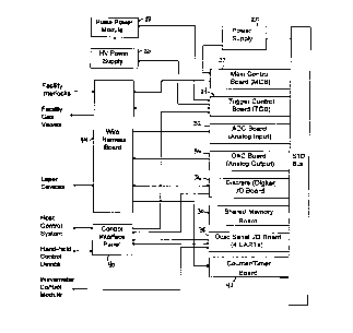
B~F.F T)FSCE~rPI'ION OF THF. DRAW~G
Figure 1 is a block diagram of the gas ~ h~rge laser controller of the
present invenffon.
DF.T.A~.F.D DF.SC~I ION OF THF. Tl~ TION
Referring now bo Figure 1, the gas ~ rh~rge laser control system of the
present invenffon is constructed around a popular bus structure, spe~ifi~lly in
20 the ~refel,æd embodiment, the STD bus, in the form of a card cage acce~ling STD
bus compatible commercially available card level components for the system. In
that regard, power for the system is provided by power supply 20, which
provides power to the power lines of the bus structure for powering the other
boards in the :.r:,t~
2~; A gas ~ rge laser control system in accordance with ff~e present
invenffon will include a main control board 22, containing a ~rocessor and
associated support circuitry, which will funcffon as the master processor in thesystem. In the preferred embodiment, ~e main control board 22 is a single board
- 21 9462q
computer having, at a minimum, an Intel type 486 processor with a minimum of
25 MHz clock speed, 128 Kbytes of battery backed-up RAM (random access
memory), at least 512 Kbytes of flash memory and at least 512 Kbytes DRAM.
This STD-80/MPX compatible processor board will have the capability of
becoming a bus master in a multi-processor environment. Those skilled in the artwill recognize that as operational demands increase for the laser control a,~al~microprocessors which are faster and more powerful and with larger memoAes
will be re~uired in the configuration specified herein.
Also included in the gas ~ rge laser control system is a trigger control
board 24, which operating on its own program, will control a separate high
voltage power supply 26 and the pulse power module 28 to provide the pulse
control and trigger for each pulse of the laser. In the p~.led embodiment, the
trigger control board (TCB) is also a single board computer having, at a
minimum, an Intel type 486 ~l ocessor with a minimum of 25 MHz clock speed, at
least 128 Kbytes of battery-b~ ^~.~ RAM, at least 512 Kbytes of flash memory andat least 512 Kbytes DRAM. This STD-80/MPX compatible l,rocessor board will
also have the capability of becoming a bus master in a multi-processor
envirolunent. An SBX high speed serial/parallel I/O board is also provided
which resides on the TCB for pulse-to-pulse interface capability.
The memory on the main control board 22 is dedicated for use by the
processor on that board. As specified herein, the processor is at least a 486
processor. Similarly, the memory on the trigger control board 24 is dedicated for
use by at least a 486 ~rocessor on that board. In addition, however, an additional
memory board 30 is provided on the STD bus for shared use by the p.ocessora on
the main control board 22 and the trigger control board 24. In that regard, the
shared memory 30 in the ~fe,l~d embo~liment is a memory card cont~ining at
least 64 Kbytes of RAM in the SI D bus card cage. It has an address space
separate and apart from the address space of the memory on the main control
board 22 and the memory on the trigger control board 24, but still within the total
address space of the processors on these boards. In this way, data as well as
21 9462q
programs may be exchanged between processors by a first processor, such as the
processor on the main control board 22, writing such dab into the shared
memory 30 from which the same may be read by another processor, such as the
l,rocessor on the trigger control board 24. Further debils of this exchange and the
5 acffvity on the STD bus in general will be subsequently described.
The laser control s~tel.~ of the ~refelled embodiment also includes an
analog-to-digibl converter board 32 for receiving analog inputs, and a digibl-to-
analog converter board 34 for outputting analog signals. The analog input board
32 in the ~f~.læd embodiment conbins thirty-two 12-bit analog input channels,
10 mulffplexed into a single 12-bit analog-to-digibl (A/D) converter. Those skilled
in the art will recognize that thirty-two rh~nn~lc was a design choice, and that the
number of channels for a parffcular application may vary based upon operational
requirements. The output of the analog-to-digital converter board 32 is a~cP5~ible
by the processors on the main control board 22 and the trigger control board 24 as
15 an V mapped card. The digital-to-analog converter board 34 in the ~re~llæd
embodiment contains eight separate 12-bit digital-to-analog ouLput channels, it
too being accessible by both processors as an I/O mapped card on the SI D bus.
As previously stated, eight channels was a design choice which those skilled in
the art will recognize may vary depending upon operaffonal requirements. There
20 is also provided a second thirty-two channel A/D converter board, spe~fi~lly
dedicated to trigger control board 24.
Also included in the SI D bus card cage is a discreet digital V board 36
and a quad serial V board 38. The discreet digital I/O board in the ~elled
embodiment provides a plurality of decoded (dedicated) I/O lines suitable for
25 various functions. By way of specific example, in the plefel.~l embodiment, the
discreet digital I/O board 36 provides control of such things as the shutter, a
dedicated line having only two states, open and closed.
A control interface panel 40 is provided for communicating with and
receiving instructions from a host control system, or alterna~vely, receiving
30 instructions from a hand-held control device. In general, the host cont~ol system
-7--
21 94629
and/or hand-held control device provides a customer-defined interface generally
including certain dedicated or decoded lines for control signals such as a trigger
signal when the same is provided externally to the laser control system of the
present invention. Such signals, other than a trigger command itself, are
provided to the discreet digital I/O board 36 through the control interface panel
40 as decoded digital signals. In that regard, in one mode of operation the trigger
command may come from the host control system, or the hand-held control
device, with the trigger comm~n~ being provided through the control in~rface
panel 40 to directly trigger the trigger control board 24 without intervenffon of
the processor on the main control board 22 or use of the STD bus, all of course in
accordance with software then operating in the trigger control board 24 in
accordance with this mode.
The quad serial V board 38 in the ~fel.~d embodiment contains four
UARrs (~ iv~rsal asynchronous receiv~l/transmitters) to provide RS 232
communicaffon capabiliffes to and from the laser control system in addiffon to the
two RS-232 communicaffon ports located on the processor. This type of
communication with a system is useful not only for initialization ~ur~Joses~ butalso for providing informaffon to the host system regarding laser status and
operaffon as the system is operaffng.
Finally, also located in the SID bus card cage is a progr~mmable
counter/ffmer board 42 providing progr~mmable timers for the main control
board 22 and the trigger control board 24, as well as counters to count events of
other devices in the system such as the hn inside the chamber.
Most of the laser functions are mo~ulored and/or controlled either directly
from the main control board 22 or the trigger control board 24 through a wire
harness board 44 col,},lel to the various monitoring and control devices, or by
one of these boards through the SI D bus and through the analog-to-digital
converter board 32, the digital-to-analog converter board 34 counter and timer
boards, and/or the discreet digital I/O board 36. In that regard, the analog-to-digital converter board provides the ability to interpret analog monitoring signals
~1 94629
from the laser system, with the digihl-to-analog converter board 34 providing the
ability to output analog control signals for controlling analog propoffional control
devices in the laser system.
The reason each procP~sor board includes its own dedicated I/O resources
5 is to keep contention for the shared V resources on the STD bus to a minimum.In that regard, in the ~,efe.led embodiment of the present invention, the
processors use a bus arbitration scheme as defined by the STLJ 80-MPX s~n~l~rd.
At power-up, the highest priority processor, the master, gains control of the bus.
Once the master finishes initiali7~tion, conhrol is passed to the first slave
10 ~rocessor. While the embodiment described herein only includes a single slave processor, this embodiment will accommodate up to seven processors.
Accordingly, if more than one slave ~rocessor is used, the initialization process
will continue until all slave ~rocessors have been inih~li7P~ When the last slave
processor has been inih~li7P~, then the first slave processor establishes
15 communications with the master and requests its program to be loaded. The
master then hransfers program data to a specific location in shared memory in
discrete chunks, such as 2 Kbytes, ~ign~ling the slave that data is available upon
completion of the hransfer of each discrete chunk. The master then waits for theslave to load the program data and signal back for more. This process repeats
20 unffl the entire program is loaded. The ~cessors then begin operating
independently, with each ~rocessor constantly ~ ing shared memory for
informaffon from each other. Alternatively, an inlL.l .lpt scheme may be
implemented for data passing between l,rocessors, providing a more ~ffl~i ~nt
transfer mechanism and relieving the back plane of the STLl card cage of a lot of
25 otherwise l-nnecf~!ss~ry signal hraffic.
The advantage rP~li7Pfl is that the yrocesso~s in the gas discharge laser
control system of the present invention are configured to serve distinct and
different ~ oses. The master E,rocessor has a real-time operating system which,
in one embodiment, has approximately 32 tasks under its control. These tasks are30 database managers, I/O monitoring routines, post-serial and parallel interface
- 21 946~9
managers, user interface tasks, inter-processor data passing tasks, laser gas
management and monitoring chamber temperature control, interlock monitoring
and lepo. Iillg, laser state managing, and others. These tasks are generaUy
characterized as the slow, less timffritical tasks within the laser control system.
The trigger control processor, the only slave processor in the specific
embodiment described, has the ve~r time-critical tasks, such as the high voltageprofiling, energy control, laser repetition rate, high speed user interface, and any
laser pulse-to-laser pulse procPcsin~ that needs to be done. As previously
discussed, however, up to seven processors may be dedicated to the h~n~lling of
very time~ritical tasks. As a matter of comparison, in the embodiment described
herein, the host ~rocessor operates on a 5 milli~cond time base, with event
timing accuracies of approximately ilO milliceconds, whereas the slave processoroperates on a 100 mi~lose~o,.d time base, with timing accuracies in the ilO
nanosecond range.
The processor on the trigger control board does not have a real-time
operating system, but in a plef~.led embodiment has a program written in a high
level programming language, such as C, and takes complete control of aU
onboard resources as needed. The master processor, on the other hand, uses its
real-time operating system to manage system resources so that it can concentrateon handling the complex task of managing the laser system and coordinating the
many tasks needed to do this s~rcPcsfully. Specific master tasks may include:
Receive key ~n~sses from the hand-held terminal (RS 232)
Display dah on the hand-held terminal (RS 232)
Receive comm~n~ from the host system (RS 232)
Send replies to the host ~ysle~l (RS 23V
Receive commands from the host system (paraUel lines)
Send shtus information to host system (paraUel lines)
Monitor and control the shutter
Monitor and control gas system valves and vacuum pump to implement
automated gas procedures
-10-
2 1 94629
.,
Monitor maintenance intervals and lifetimes of various laser hardware
modules
Monitor safety interlock switches
Control safety lamps mo~u~le.i on top of laser
Manage several data bases:
Pulse-to-pulse data
Configuraffon data
Operating parameters
V data (analog and pulæ inputs)
System errors
Monitor metal fluoride trap
Monitor and control chamber blower hn
Monitor and control chamber gas temperatur~
Monitor High Voltage pulse power supply
Monitor laær exhaust vent flow
Monitor nitrogen gas supply p~
Monitor cooling water temperature
Monitor pulse-to-pulse log data for long term trend changes to determine
err~liveness of chamber gas
Send commands to trigger (slave) processor
Receive data from trigger (slave) processor
Control laær states of re~1in~ffs
Monitor and control line narrowing control subar~
While the present invention has been ~i~lo5e 1 and described with 1 2s~l
to a certain ~refe.l~l embodiment thereof, it will be understood by those skilled
in the art that the preænt invention may be altered in various ways and rP~li
in various embodiments without departing from the spirit and scope thereof.