Note: Descriptions are shown in the official language in which they were submitted.
~ W0 96/029~4 2 1 9 4 8 6 5 r~
SINGLE AND MULTI-LAYER
VARIABLE VOLTAGE PROTECTION DEVICES AND
METHODS OF MAKING SAME
Field of the Invention
The present invention relates generally to variable voltage
protection devices used to protect electronic circuits from overvoltage
L~n~lsie"L~ caused by lightning, ele~l,u",a~"~lk; pulses, eleullu:,Ld9c
di:,~harues, ground loop induced transients, or inductive power surges.
The present invention relates particularly to materials of construction
for variable voltage protection components and methods of making
variable voltage protection components and devices.
Background of the Invention
Voltage transients can induce very high currents and voltages
that can penetrate electrical devices and damage them, either causing
hardware damage, such as semiconductor burnout, or electronic upset,
such as l,~,r,s",;s~io,l loss or loss of stored data. The voltage
l,dnsie,,l~ produce large voltage spikes with high peak currents (i.e,
. overvoltage). The three basic overvoltage threats are electrostatic
- discharge, line lldn~ , and lightning. Cle~,~lu:,~d~ic discharge
typically occurs when static charge dissipates off the body of a person
in direct physical contact with an operating electronic system or an
individual component, such as an integrated circuit chip. Line
~Idnsie"~ are surges in AC power lines. Line transients can also occur
due to closing a switch or starting a motor. Lightning strikes can strike
stationary objects; such as a building, or mobile objects such as
aircraft or cellular phones. Such strikes can suddenly overload a
system's elel~un,~s. At peak power, each of these threats is capable
of destroying the sensitive structure of an integrated circuit chip.
Various overvoltage protection materials have been used
30 previously. These materials are also known as nonlinear ~ .ldnce
WO 96102924 2 1 9 ~ 8 1~ ~ p
, .. .
-2--
materials and are herein referred to as volta~e variable materials. In
operation, the voltage variable material initially has high eiectrical
resistance. When the circuit experiences an overvoltage spike, the
voltage variable material quickiy changes to a low electrical resistance
state in order to short the overvoltage to a ground. After the
overvoltage has passed, the material immediately reverts back to a
high electrical resistance state. The key operational parameters of the
voltage variable material are the response time, the clamp voltage, the
voltage peak and pealc power. The time it takes for the voltage
variable material to switch from insulating to conducting is the
response time. The voltage at which the voltage variable material
limits the voltage surge is called the clamp voltage. In other words,
after the material switches to conducting, the material ensures that the
integrated circuit chip, for example, will not be subjected to a voltage
greater than the clamp voltage. The voltage at which the volta~e
variable material will switch (under surge con~liLions) from insulating to
conducting is the switch voltage. These materials typically comprise
finely divided conductive or semiconductive particles dispersed in an
organic resin or other insulating medium. For example, U.S. Patent No.
3,685,026 (Wakabayashi, et al.), U.S. Patent No. 4,977,357 (Shrier)
and U.S. Patent No. 4,726,991 (Hyatt et al.) disclose such materials.
Voltage variable materials and components containin~q voltage
variable materials have been incorporated into overvoltage pru~ lion
devices in a number of ways. For example, U.S. Patent No.
5,142,263 and 5,189,387 (both issued to Childers et al.) disclose a
surface mount device which includes a pair of conductive sheets and
voltage variable material disposed between the pair of conductive
sheets. U.S. Patent No. 4,928,199 (Diaz et al.) discloses an integrated
circuit chip package which comprises a lead frame, an integrated
circuit chip protected by an electrode cover which is connected to
ground on one side, and a variable voltage switching device including
~ W0 96~02924 2 1 ~ 4 8 6 ~ r~
the voltage variable material connected to the electrode cover on the
other side. U.S. Patent No. 5,246,388 ~Collins et al.) is directed to a
device having a first set of electrical contacts that interconnect with
signal contacts of an electrical connector, a second set of contacts
5 that connect to a ground, and a rigid plastic housing holding the first
and second set of contacts so that there is a precise spacing gap to be
filled with the overvoltage material. U.S. Patent No. 5,248,517 (Shrier
et al.) discloses painting or printing the voltage variable material onto a
substrate so that conformal coating with voltage variable material of
10 large areas and intricate surfaces can be achieved. By directly printing
the voltage variable material onto a substrate, the voltage variable
material functions as a discreet device or as part of associated
circuitry.
The above U.S. Patents referred to are incorporated herein by
1 5 reference.
Although the prior art discloses various materials and devices,
there is a continuing and long felt need to provide improved cost-
effective voltage variable materials and devices of more consistent
performance properties to prevent variations in the clamp voltage under
20 various conditions in which the materials and devices are used.
Summarv of the Invention
This invention co"l,uri~es in one aspect a variable voltage
protection device which co"lpfises a single layer of neat dielectric
polymer, glass or ceramic positioned between a ground plane and an
25 electrical conductor of an electronic device. It has surprisingly been
found that overvoltage protection can be effectively provided by such a
polymer, glass or ceramic layer, provided that the polymer, glass or
ceramic layer is sufficiently thin to provide the switching and the
voltage clamping chald~L~d~LiGs desired for a given protective device
30 for a given electronic device. It has been found that for certain
W0 96/02924 21~ 48 ~ r.~
. ~ .
. ,.~4, . .
polymers the thickness must be less than about 0.0406 mm (1.6 mils)
and for other polymers the thickness must be less than about 0.0203
mm (0.8 mil), preferably less than about 0.0127 mm (0.5 mil~ and
more preferably less than about 0.0051 mm (0.2 mil). For certain
5 glasses and ceramics the thickness must be less than about 0.127 mm
(5 mils), preferably less than about 0.0965 mm (3.8 mils) and more
preferably less than about 0.0406 mm (1.6 mils), with thicknesses less
than 0.0203 mm (0.8 mil) preferred in many applications.
In another aspect of the pre.sent invention, superior pe~ru""a"ce
10 can be provided by a variable voltage protection component which
comprises the combination of (a) a layer of variable voltage p,uleclion
materlal comprising a binder containing conductive partlcles and/or
se",iconductive particles; and (b) a layer of neat dielectrlc polymer,
glass or ceramic in contact with one surface of said layer of variable
15 voltage material; wherein the neat dielectric polymer, glass or ceramic
layer Is present in a thickness of less than about 0.0406 mm (1.6
mils). The presence of the thin layer of neat dielectric polymer, glass
or ceramic on the surface of the binder/particle type of variable voltage
p~uL~l,Lion material provides a component having desirable voitage
20 clamping properties, as well as other desirable properties.
In another aspect, this invention provides a layered variable
voltage protection component comprising a first layer of variable
voltage protection material comprising a binder having dispersed
therein at least about 20% by volume of conductive or semlconductive
25 particles; a second layer of variable voltage pruL~uLion material in
contact with the first layer comprising a binder having dispersed
therein at least 40~/0 by volume of conductive or semiconductive
particles; and a third layer of variable voltarJe p,uL~uLiu" material in
contact with said second layer comprising a binder having dispersed
30 therein at least 20% by volume of conductive or semiconductive
particles. It has been found that the multiple layer constructlon
WO 96102924 2 ~ 9 4 8 6 ~ r~
_5
provides an opportunity to vary the conductor particle loading and/or
semiconductor particle loading in each layer, such that the outer layers
contain lower particle loadings than the inner layer, in order to achieve
a wide range of clamping voltages and other desired properties. In an
5 additional aspect of this invention, the outer layer in contact with the
electrical conductor of the electronic device should have a lower
particle loading than the inner layer with a higher particle loading, but
in such case the other outer layer in contact with the ground plane can
be higher or lower in particle loading. In an additional aspect of this
10 invention, this multi-layer variable voltage protection component can
further be provided with a thin layer of the neat dielectric polymer,
glass or ceramic as referred to above on one outside surface or both
outside surfaces, in order to provide additional p,upe, lies and
characteristics of the co"lponer,L. In this aspect of the invention, the
15 layer on the side of the electrical conductor can have a higher or lower
particle loading than the inner layer provided the neat dielectric
polymer, glass or ceramic layer is positioned between the outer layer
and the electrical conductor. In another aspect of this invention this
multiple layer component can be provided with a conductive, e.g.,
20 metal, layer interposed between the first layer and second layer and/or
between the second layer and third layer of variable voltage protection
material. In yet another aspect of this invention, these multiple layer
components li,e"~selves can be stacked, with or without the outer
layers of neat dielectric polymer, glass or ceramic layers, and with or
25 without an intervening layer of neat dielectric polymer, glass or ceramic
between components to achieve desired performance cl-ald.,~t:li ,lics.
In another aspect, this invention provides a method of making a
variablç voltage protection material comprising forming a mixture
~ co,,,,uri:~i,,g (a) conductive, semiconductive and/or insulative particles
30 and (b) colloidal insulating particles in (c) a light organic solvent; mixingsaid mixture to disperse the colloidal insulating particles in the
_ _ _ . ... ..
21~,86S
WO 96/02924 ' r_l~a,.
- 6 ~
conductive/ semiconductive/insulative particles; evaporating at least a
portion, preferably all, of the solvent; and mixing the resultant mixture
of conductive/semiconductive/insulative particles and colloidal
insulating particles with a binder to form a variable voltage protection
5 material.
Brief Des.,,iution of the Drawings
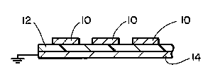
Figure 1 is a cross-section view of an illustration of a variable
voltage protection device incorporating a layer of neat dielectric
polymer, glass or ceramic.
Figure 2 is a cross-section view of an illustration of a variable
voltage protection compound having a layer of variable volld~ nldL~ddl
comprising a binder and conductive particles, se"licondL~ctive particles
and/or insulative particles in combination with a layer of neat dielectric
polymer, glass or ceramic.
Figure 3 is a cross section view of an illustration of a multi-layer
variable voltage protection compor ent according to this invention and
illCOI,uOldlillg optional exterior layer of neat dielectric polymer, glass or
ceramic .
Figure 4 is a cross-section view of an illustration of a multiple
20 layer variable voltage p,ol,:~,Lion camponent according to this invention
ill~,OI,uOldLillg optional interposed metal layers between the layers of
variable voltage protection material.
DetR~ Des~.,iuliun of the Invention
Referring to the first aspect of this invention which comprises a
25 variable voltage protection device comprising as the variable voltage
protection material a thin layer of a neat dielectric polymer, glass or
ceramic, it has been found that such a device is surprisingly effective
at a desired range of clamping voltages provided that the layer of neat
dielectric polymer, glass or ceramic is sufficiently thin. For some
WO 961029~4 2 ~ 9 l 8 65 r~l,u~ ~
7--
polymers a layer of less than about 0.0203 mm (0.8 mil) will provide
effective overvoltage protection under various conditions, while for
other polymers a layer of less than about 0.0406 mm (1.6 mils)
provides the desired pel ru~ ~uance cha,dl,L~ ius. It is preferable in
5 many variable voltage protection ~F~i lions that the polymer layer be
less than about 0.0127 mm (0.5 mill and more preferably less than
about 0.0051 mm (0.2 mil). Similarly, when the layer is a glass or
ceramic, it is preferred that the layer be less than about 0.0203 mm
(0.8 mil), but for some ,qlasses in certain applications a thickness of up
to about 0.0965 mm (3.8 mils) is applup,idL~. As will be apprt:-,id~ed
by one skilled in the art, the actual thickness of the neat dielectric
polymer, glass or ceramic layer employed in a particular variable
voltage protection function will vary depending on the type of polymer,
glass or ceramic used, its dielectric prupe, lies, the operating cond;lions
of the device in which the variable voltage prul~.,lion element is
employed and the pe,ro""dnce p~upelLies required of the protection
device .
Fig. 1 illustrates the device of this invention where layer 12 is
positioned between electrical conductors 10 and ~qround plane 14.
As used in the disclosure and description of the present
invention, the term "neat dielectric polymer, glass or ceramic" refers to
a polymeric, glass or ceramic material which can act as a dielectric or
insulating material under the normal voltage and current conditions of
intended use and which is unfilled, i.e., does not contain conductive or
semiconductive particles such as those typically used in binders or
otherwise dssocidLed with variable voltage p,uLe~Lion materials of the
prior art. However, "neat dielectric polymer, glass or ceramic" is
intended to include polymeric, glass or ceramic materials which fulfill
the above criteria, but which may contain or have added to them
insulative or inert particles or materials that are inactive or do not
interfere with the desired dielectric/variable voltage p~ul~,lion
wos6/02s24 21~ 6~ r~
properties of the polymer, glass or ceramic layer as used in the present
invention. The polymer, glass or ceramic layer useful in the present
invention can be formed or cured in situ or can be;provided in a
preformed or procured sheet or film and placed In position for use
5 according to this invention. Additionally, thé polymer layer can be a
pre-cured polymer block from which sheets or layers of polymer can be
sliced or shaved in the desired thickness. Further, the polymer, glass
or ceramic layer can be provided in the form of a mat of polymer, glass
or ceramic fibers or particles which are co"".,dssed or otherwise
10 treated to provide the polymer, glass or ceramic layer in the desired
thickness and properties for use in this invention. Such a mat, which
may contain an adhesive or binder for the fibers can be heated or heat
treated while compressed to provide a sheet of polymer, glass or
ceramic fibers of desired thickness for use in this invention.
The polymers, glasses and ceramics useful in this aspect of the
invention can be selected from polymers known in the art to be useful
as binders in conventional variable voltage protection materials to the
extent that such polymers are known to have high resistance to
tracking and high ~ allce to arcing. In addition, other polymers,
glasses and ceramics not previously suitable for or used as such
binders are also useful in the present invention if they exhibit sufficient
dielectric p~uperLies~ sufficient l~ "ance to tracking and sufficient
lance to arcing under the operating conditions selected for a
device according to this invention.
In general, the types of dielectric polymers useful in the present
invention include silicone rubber and elastomer, natural rubber,
organopolysiloxane, polyethylene, polypropylene, polystyrene,
poly(methyl methacrylate), polyacrylonitrile, polyacetal, polycarbonate,
polyamide, polyester, phenol-formaldehyde resin, epoxy resin, alkyd
resin, polyurethane, polyimide, phenoxy resin, polysulfide resin,
polyphenylene oxide resin, polyvinyl chloride, fluoropolymer and
~ W096102924 219~6~ r~
chlorofluoropolymer. These and other useful polymers can be used by
themselves or can include various substituent ~roups and can be
mixtures, blends or copolymers thereof, wherein the final polymer is
selected in accordance with the criteria described above. A particularly
5 preferred polymer is a conventional and col,l"lerui.,lly available General
Electric "615" silicone, and it is also particularly preferred to cure this
polymer for about 15 minutes at about 200~C to obtain p,uperli~s
better suited for use in this invention. In such a p,~pa,dlion, the
curable liquid polymer is coated on the desired ground plane to the
10 desired thickness, then cured as indicated. The cured polymer layer is
then placed in contact with the electrical conductor~s~ of an electronic
device to form the variable voltage plu~ ion device of this invention.
It has been found that this polymer provides good pe~ruul'd''ce in a
thickness of about 0.0051 mm (0.2 mil). Another form of polymer
15 useful in this invention is woven or nonwoven polymer fibers
co,,,,u~t~s~ed into a mat of desired thickness. For example, a polymer
fiber material useful in the present invention is a layer of nonwoven
aramid (aromatic polyamide) fibers, co"""err '~y available as
"KEVLAR" or "NOMEX" nonwoven fiber mat from E.l. Du Pont de
20 Nemours & Company. The nonwoven aramid fiber mat of about
0.0406 mm (1.6 mils) has been found to provide good pe"u""ance
when cor"~ ssed to a thickness of 0.0203 mm (0.8 mils~.
The dielectric glass materials useful in this invention are likewise
glass materials which have been used as binders in variable voltage
25 materials such as sodium silicate. As with the polymer type material,
the ~qlass material can be either coated on or formed in place on the
desired substrate, such as the ground plane, or can be p,~u""ed in a
sheet and assembled between the ground plane and the electrical
~ conductor to form the device of this invention. The dielectric ~qlass,
30 such as a sodium silicate is generally useful in this invention in
~h;ukllesses similar to those outlined above for the polymer materials,
WO96/02924 219d~865 r~
1 o
but is also useful in some instances in thicker layers, e.g., up to about
0.127 mm l5 mils), but usually less than about 0.0965 mm (3.8 mils~
and preferably less than about 0.0406 mm (1.6 mils). Further, glass
fibers can be used to form the dielectric glass layer in accordance with
this invention. For example, a fiberglass mat can be co"",,~ ,~ed to the
desired thickness, e.g., about 0.0254 mm (1 mil) or less, to provide
the performance "ha,dl,Led~Lics desired for a particular application in
which this invention is to be used. As with the polymer fiber mat, a
sheet of nonwoven or woven glass fibers can be co"",,~ssed, with or
without an adhesive or binder present, to the desired thickness under
heat treatment to provide a result sheet of desired thickness for use in
this invention.
The dielectric ceramics useful in this invention are glass-
ceramics, devitrified glasses, crystallized glasses, crystalline ceramics,
crystalline ceramic co"~posil~s and diamond. While diamond is not
lechl1ically a ceramic, it is included here within the definition of
dielectric ceramic" because it possesses the dielectric properties of
conventional ceramics which are useful in this invention. Thus,
preferred ceramic materials for use in this invention are aluminum
oxides and aluminum nitride, crystalline ceramic co"",o:,iL~, include
those which include AIN, Al203, Si3N4 and TiN. As noted above for
glasses, the ceramics can be used in this invention up to about 0.127
mm (5 mils), usually less than about 0.0965 mm (3.8 mils) and
prert:rdbly less than 0.0406 mm (1.6 mils).
As used herein "glass" is intended to include the amorphous
type glasses and "ceramic" is intended to include the crystalline type
glasses and ceramics and diamond crystals. In addition to the above
methods of assembly, fabrication and use, it will be recognized by one
skilled in the art that the layer of glass and ceramic can be applied for
use in this invention by various known methods, such as solvent
W096102924 2194~6~ P~l/u~ 5~
deposition, sol-gel coating, sputtering, evaporation, chemical vapor
deposition, plasma spraying, anodizing and the like.
As will be appreciated by one skilled in the art, various dielectric
polymers, glasses and ceramics can be selected and used in this
5 invention following the teachings contained herein with respect to the
thickness that must be maintained for the neat dielectric polymer, glass
or ceramic to exhibit the desired clampiny voltage and other desired
properties. Examples of polymers which can be employed in this
invention include those disclosed in U.S. Patent Nos. 4,298,416,
4,483,973, 4,499,234, 4,514,529, 4,523rO01, 4,554,338,
4,563,498, 4,580,794, the disclosures of which are incorporated
herein by reference. As indicated, other resins may be selected for use
in accordance with this invention.
In another aspect of this invention, it has been found that the
15 above described neat dielectric polymer, glass or ceramic layer can be
used in combination with a variable voltage material to modify and
enhance certain prupe,5es and pe,fu""anceclla,a~ ,Li,,:, of the
variable voltage material. As referred to as part of this invention, the
variable voltage material can be a conventional variable voltage
20 material which co""~ri ,e5 a binder c~llL.,:.Iillg conductive particles
and/or semiconductive particles andlor insulative particles mixed with
or treated with colloidal insulating particles as disclosed herein. As
used in this invention, the variable voltage material may a!so include
other novel, modified and improved variable voltage materials or
25 variable voltage components such as disclosed in this speciri-,aLion and
as disclosed in U.S. application Serial No.08/275,947 filed on 14 July
1994. The neat dielectric polymer, glass or ceramic layer which is
used in combination with such variable voltage materials or
co""~ol1e"L~ is placed in contact with one or both surfaces of the
30 variable voltage material or component and can be the same neat
WO 96/02924 21 9 4 8 6 ~ r~
,, ,. ~2~,
dielectric polymer, glass or ceramic referred to and described above in
this application.
Fig. 2 illustrates the device of this invention where neat
dielectric polymer, glass or ceramic layer 12 is positioned between
5 electrical conductors 10 and variable voltage material 13. Ground
plane 14 is provided in contact with layer 13.
In this aspect of the invention, the above-described neat
dielectric polymer, glass or ceramic layer can be applied to the surface
of a desired variable voltage material or component as described
10 above, for example in a liquid form and cured in place, or can be
provided in a pre-cured or pre-formed sheet and laminated to the
surface of the variable voltage material or component. It will be
recognized by one skilled in the art that various conventional variable
voltage materials and components can be combined with the neat
15 dielectric polymer, glass or ceramic layer as described herein to form
the co"ll,i"d~ion of this invention, a variable voltage material with an
exterior layer of neat dielectric polymer, glass or ceramic, to provide
desired performance characteristics. In particular, it is preferred in this
aspect of the invention to provide in col"b;"d~ion a multi-layer product
20 as described below and a neat dieiectric polymer, glass or ceramic
layer on one or both exterior surfaces of such a multi-layer variable
voltage component.
In another aspect this invention co""~(ises a multi-layer variable
voltage protection component which ColllplisG-s at least three iayers of
25 variable voltage material which comprises a binder containing
conductive, semiconductive and/or insulative particles and may
optionally contain colloidal insulative particles. The multi-layer variable
voltage protection component according to this invention comprises
two outer layers COllLdill;ll9 a lower loading or conce"L~dLion of
30 conductive, semiconductive and/or insulative particles while the inner
layer of the co"~pone"L contains a higher loading or conce"L~dLion of
W0961029Z4 ~lg~1~6
~' ,1, -13-
conductive, semiconductive and/or insulative particles. As described
above, this multi-layer variable voltase protection component can
optionally further comprise on either or both surfaces of the
component, a neat dielectric polymer, slass or ceramic layer to further
5 enhance or chanse the performance chala~ ,Lics as desired.
Fi~. 3 illustrates this invention where individual layers of variable
voltase protection material 15, 16 and 17 form the multi-layer product
positioned between electrical conductors 10 and sround plane 14.
Optionally, a neat dielectric polymer, slass or ceramic layer 12 can be
10 positioned on the outside layer 15 and in contact with conductors 10
and/or neat dielectric polymer, glass or ceramic layer 12' can be
positioned on the outside of layer 17 and in contact with sround plane
14.
The individual layers of the multi-layer product of this invention
15 can be formulated as conventionally disclosed in the patents referred to
in the background section above or more preferably can be formulated
and made by the method described herein below. In general, it is
preferred that the two outside layers of the present multi-layer product
contain at least about 20 percent by volume conductive,
20 semiconductive and/or insulative particles while the inner layer
contains at least about 40 percent by volume conductive,
semiconductive and/or insulative particles in a binder. It is more
preferred that the two outside layers contain at least 30 percent by
volume of such particles and the inner layer contains at least about 50
25 percent and more preferably at least about 60 percent by volume of
such particles in the binder. It is not necessary for the two outside
Iayers of the product to contain the same loading or concentration of
such particles, for example, one outside layer may contain 30 percent
by volume of such particles while the other outside layer contains 40
30 percent and the inner layer contains 60 percent by volume of such
particles in the binder. Followins the teachin~s of this invention, it will
,, _ . ... . . _ _ . ...
WO 96/02924 ~ 1 9 ~ ~ 6 5 P~
be apparent to one sl<illed in the art that the con~u~ldLiuns or loadings
of conductive, semiconductive andlor insulative particles in the various
layers can be varied to obtain the performance ul,a,duL~ s desired.
However, it will further be recognized that the teachings of this
invention indicate that the exterior layers of the component contain
lower particle loadings than the interior layer or layers. It will further
be recognized that the inner or interior layer of this component can
itself be made up of mùltiple layers of variable voltage materials which
are higher in particle loading or concentration than the exterior surface
layers.
When the first outer layer is in direct contact with the electrical
conductor of the electronic device, that outer layer has a lower
conductive/semiconductive/insulative particle loading than the inner
layer, as outlined above, but the other outer layer is optional and can
have a higher or lower particle loacling than the inner layer. When the
first outer layer co",,u,ises a layer of neat dielectric polymer, glass or
ceramic which is in contact with the electrical conductor, then the first
outer layer can have a higher or lower particle loading than the inner
layer and the other outer layer is optional and can have a higher or
lower particle loading than the inner layer.
The thickness of each layer and the overall thickness of the
multi-layer component can be d~""ined by one skilled in the art
following the present disclosure to achieve the desired perru~lllance
characteristics of the component. For example, a preferred
~ulbocli~ L comprises a first layer of 0.0254 mm ~1.0 mil) cor,L~i"i"g
30 percent by volume of conductive particles, with an inner layer of
0.0203 mm (0.8 mil~ containin~ 60 percent by volume of conductive
particles and a third layer of 0.0178 mm (0.7 mil) containing 30
percent by volume of conductive particles. Similarly, another preferred
embodiment comprises a first layer of 0.0254 mm (1.0 mil) of 30
percent by volume conductive particles, an inner layer of 0.0508 mm
~ WO96102924 2~9~6~
, , -15-
(2 mils) of 60 percent by volume conductive particles and a third layer
of 0.0203 mm (0.8 mil) of 30 percent by volume conductive particles.
Multi-layer confi,qurations such as these provide good performance
characteristics. In addition, it will be ~t:co~ui~ed by one skilled in the
5 art that each layer which is provided in the form of a polymeric or
other dielectric binder containing the desired conductive,
semiconductive, insulative and/or colloidal insulative particles contained
therein can be applied in a liquid form and then dried or cured. The
multi-layer product of this invention can be formed by applying two or
10 more of the layers and then curing or drying all of the layers
simultaneously or, alternatively, the multi-layer product of this
invention can be formed by applying the first layer, for example, to a
metal ground plane member, and curing or drying that layer before
applying the s~lhsequent layers. In this fashion, each layer can be
15 applied and cured or dried to the desired thickness before the
subsequent layer is applied. Thus, it will be recognized by one skilled
in the art that the multi-layer variable voltage p"~ ,,lion co"".one"l
according to this invention can be formed in various ways using
various materials. However, a preferred embodiment is provided by
20 employing the method described herein below for preparing the variable
voltage p~u~ ion material then forming the above multi-layer product
of this invention in the particle loadings and the layer ~ hl,e,~es as
described above. It will further be recognized by one skilled in the art
that each individual layer can be selected as desired such that each of
25 the layers of the multi-layer product may be of a different type of
binder materials and/or conductive, se",i.,ol,cluctive, insulative, or
colloidal insulative particles provided that the basic criteria is followed
in that the exterior layers of the multi-layer product contain the lower
conce"L,dLion or loading of such particles while the interior layer
30 contains a higher loading of such particles. For example, each layer
can be selected from the various conventional variable voltage
WO 96/02924 2 ~ ~ ~ 8 6~
-16-
materials available in the prior art which connprise a binder containing
various conductive and/or semiconductive and/or insulative particles.
Alternatively, it will be reco~nized $hat each layer can be individually
selected to employ the novel and irnproved variable voltage p,u~e~Lit,n
5 materials or components as disclosed herein or in U.S. d~Jplic~iLion
Serial No. 08/275,947 filed on 14 July 1994. In this regard, the novel
variable volta~e materials containin~, for example, the reinforcing mats
as disclosed in said co-pendin~ application, can be selected for use as
particular individual layers in the multi-layer product of this invention.
The multi-layer product of this invention can be constructed
such that each layer co",p, i .es a binder, such as a dielectric polymer or
dielectric glass binder, cûntainin~ conductive particles, such as
aluminum particles, and optionally containing semiconductor particles,
such as silicone carbide, and further, optionally cor,L~.;";.,~ insulative
15 particles, such as aluminum oxide ,andlor colloidal insulative particles
such as a fumed silica. Each of these various co",pone"Lb are well
known in the art as well as methods for formin~ the variable volta~e
materials with the binders and curing or drying the binders to form the
desired final material. In this repard, the disclosures of the above-
20 ,t:r~ nced patents are incorporated herein as providing the basicmaterials and components which can be used to make the multi-layer
product accordinp to the present invention.
For use in this invention "conductive particles" include metal
particles, such as copper, aluminum, molybdenum, and the like or other
25 conductive materials such as carbon black, carbonyl nickel, tantalum
carbide, and the like. "Semiconductive particles" include silicon
carbide, beryllium carbide, calcium oxide, and the like. "Insulative
particles" include aluminum oxide, plass spheres, calcium carbonate,
barium sulphate, and the like. "Colloidal insulative particles" include
30 the colloidal form of fumed silica, kaolin, kaolinite, aluminum trihydrate,
feld spar, and the like. Reference is made to U.S. Patent No.
~ W0 96/02924 2 1 9 ~ ~ 6 5 r ~
-17-
4,726,991 for further examples of specific particles and materials in
each category which are useful in this invention following the
procedures and teachings set forth herein.
Fig. 4 illustrates this invention where individual layers of variable
voltage protection material 15, 16 and 17 are separated by optional
metal layers 18 and 18', which together comprise the multi-layer
variable voltage protection device positioned between electrical
conductors 10 and ground plane 14.
In another aspect, this invention co",~.dses an improved method
of making a variable voltage p~uLt~ iun material containing a binder and
conductive particles and/or semiconductive particles in cor,~ Liun
with insulative particles and colloidal insulative particles all dispersed in
the binder. As mentioned above, each of these cor,,~.une,,L~ of binder,
conductive particles, semiconductive particles, insulative particles and
colloidal insulative particles are known in the art and are described in
various detail in the patents ~t:rt~l~nced above. The present aspect of
this invention involves novel methods of combining these conventional
materials to produce novel variable voltage p,ul~,lion materials having
enhanced p, upe, Lies. The methods of the present invention comprise a
step of dispersing the conductive and/or insulative particles and the
desired amount of colloidal insulative particles in an organic solvent
whereby the conductive/insulative particles and the colloidal insulative
particles are thoroughly dispersed in the solvent mixture. The particles
can be added to the solvent in any desired order, but it is generally
preferred to disperse the conductive and/or insulative particles in the
solvent first, then add the colloidal insulative particles. The mixture is
then dried by removing the solvent by evaporation. The dried mixture
of particles is usually in the form of a cake, which is then ground to a
powder in a grinder. The resulting powder is then added to a dielectric
polymer binder in a milling process to uniformly disperse the particles
throughout the dielectric polymer. For example, the conductive particle
wo 96/02924 ~ 1 9 d~ 8 ~5 r~
18
can be aluminum, the insulative particle aluminum oxide, the colloidal
insulative particle fumed silica and the s.olvent methyl ethyl ketone. In
some formulations it is preferred to also include glass fibers as
sdditional insulative particles. In a preferred aspect, the method
5 further comprises forming a first solvent mixture of just conductive
particles and colloidal insulative particles, and forming a second solvent
mixture of insulative particles and r,olloidal insulated particles. Both
mixtures are separately dried; the resulting two dry mixtures are
sepa,d~uly ground then added simultaneously to a mill to be mixed in a
10 polymer binder to form a desired v,ariable voltage pru~e,,liun material.
In a preferred method, the binder-particle mixture is mixed with
an excess of a strong pûlar solvemt, such as MEK, to swell the binder.
This mixture is then mixed in a high speed mixer to form a viscus
material similar to a pigmented paint. This final mixture can be applied
15 as desired to form variable voltage pru~ ion co",~.one"Ls or layers by
o ,ili"g the material as desired in layers of desired thickness and
allowing the solvent to evaporate and allowing the binder to further
cure leaving the desired layer of variable voltage protection material.
In a preferred formulation, STI Dow Corning fluor~ " - le rubber
20 ~DC-LS2840) is used in col"l,i.,dLion with a STI Dow Corning
polydimethylsiloxane (HA2) in a volume ration of about 4:1. This
mixture is milled until it becomes uniform and essentially translucent.
At that point, a mixture prepared of aluminum oxide and fumed silica
particles is added to the mill. The pl~pdldLiull of the mixture of
25 aluminum oxide particles and fumed silica particles is as follows. A
preferred aluminum oxide particle is a 5 micron "A14" particle from
Alcoa. This particle is dispersed in methyl alcohol and the particle-
solvent mixture passed through a 10 micron screen. To the resulting
solvent d;~per~ioll of aluminum oxide particles is added J ~/0 by weight
30 (based on the initial weight of the aluminum oxide) of a fumed silica
~ W0 9610~9~4 21 g ~ 8 ~ ~ r~
-19-
particle, which is "Cabosil T5530" pledi,pe,~ed in methyl alcohol and
mixed until evenly dispersed through the solvent mixture. The solvent
is then removed through evaporation to form a cake. The dried
aluminum oxide particle-Cabosil cake is then ground to a powder. A
5 second solvent mixture of an aluminum particle desi~ dLt:d "H10" from
Alcoa, which is 10 micron particle, likewise dispersed in methyl alcohol
then mixed with 17% by weight of a fumed silica, which is "Cabosil
M5". As above, the H10 aluminum particles are dispersed in the
methyl alcohol and screened through a 20 micron screen, then the
10 Cabosil M5 dispersed in methyl alcohol is added to the screened H10
aluminum particles in the solvent. After mixing the solvent is
evaporated to form a cake. The dried aluminum particle-Cabosil cake is
then ground to a powder. The ratio of aluminum particles to aluminum
oxide particles is about 2:1 and about 45 parts by volume of particles
15 are mixed with about 55 parts by volume of binder. Both the aluminum
and the aluminum oxide powders are added to the mill and milled into
the polymer mixture. After milling for a sufficient time, such as 30
minutes to an hour, to obtain uniform mixing, the mixture is removed
from the mill and mixed with methylethylketone solvent in a weight
20 ratio of about one part solvent per part of total mix from the mill. This
mixture is allowed to stand for a period of a few hours, such as
overnight, in the MEK, then is mixed with a small amount such as, for
example about 4~/0 by weight of a peroxide, which is 1,1-di-t-
butylperoxy-3,3,5-trimethyl cyclohexane, and 17% by weight of a
25 crosslinking agent, which is trialylisocyanurate, wherein the weight
percent is based on weight of binder. This final mixture is then mixed
at low speed to assure thorough mixing then is mixed at high speed
until the mixture becomes the consistency of a pigmented paint. This
final variable voltage ulu~,Lion co"lpo~ ioll can then be coated or
30 deposited on a ground plane or on electrical conductors or other
substrates in desired patterns, the solvents are allowed to dry and the
W0 96t02924 2 1~ 5 r~
-20-
binder allowed to further cure or crosslink. If desired, a temperature of
about 200~C for about 20 minutes can be used to assist in the drying
and curing or crosslinking of the binder. The variable voltage
p,ule~lion material is thereby provided in the desired thickness and
configuration to serve as the variable voltage protection layer or
component. This composition can be used to form the multi-layer
product invention disclosed above or in combination with the neat
dielectric polymer, glass or ceramic layer invention disclosed above.
As used in the above method aspect of this invention the
organic solvent can be any solvent in which the desired particles will
disperse and mix with other particles. In general the solvent can be a
C1 to C10 h~dlucdlbon which is substituted or unsubstituted, and
include straight and branch chain hydrocarbons, alcohols, aldehydes,
ketones, aromatics, and the like. Examples of such solvents useful in
this invention include methyl alcohol, ethyl alcohol, n- or iso-propyl
slcohol, formaldehyde, methyethyl ketone, toluene, benzene, butane,
pentane, the choloro/fuoro ethylenes ~"Freon" solvents from Du Pont),
and others. It will be recognized by one skilled in the art that a solvent
that can be readily evaporated under available conditions is desirable.
As used in the above invention the conductive particles,
semiconductive particles and insulative particles are conventional as
set forth in the above patents incorporated by reference.
The principles, preferred embodiments and modes of operation
of the present invention have been described in the foregoing
:,ue~ alion. However, the invention which is intended to be
protected is not to be construed as limited to the particular
embodiments disclosed. Further, the embodiments described herein
are to be regarded as illustrative rather than restrictive. Variations and
changes may be made by others, and equivalents employed without
departing from the spirit of the present invention, and it is expressly
intended that all such variations, changes and equivalents which fall
~ WO 96102924 2 1 9 4 8 6 5
-21 -
within the spirit and scope of the present invention as defined in the
claims be embraced thereby.