Note: Descriptions are shown in the official language in which they were submitted.
. ~ 219~a38
INTEGRATED CIRCUIT PACKAGING STRUCTURE
BACKGROUND OF THE INVENTION
The present invention relates to a package structure
for an integrated circuit, and, more particularly, to a
package structure for an integrated circuit containing a
- 5 plurality of laminated chip carriers.
Referring to FIG. 19, a conventional package for an
integrated circuit having a plurality of laminated chip
carrier comprises laminated film carriers 101a - lOld, and
outer leads 152a - 152e which the respective film carriers
lOla - 101d have. Connection of each of the outer leads
152a - 152e to a wiring board 102 depends on whether it
consists of a common terminal of each lead or a non-common
terminal.
Referring to FIG. 20, the outer lead 152e which
consists of the common terminal of each lead is soldered on
a connection terminal of the wiring board 102 by overlapping
the common terminal ends of the outer leads 151a - 151d.
Referring to FIG. 19 again, the outer leads 152a - 152d
of the film carriers 101a - 101d are the non-common terminal
ends. The outer leads 152a - 152d are connected to the
connect location on the wiring board 102 by shifting each
other.
~19~~38
2
Referring to FIG. 21, at the connect location of the
outer lead 152c, for example, the film carriers lOla, lOlb
and lOld do not have the outer leads. Only the film carrier
lOlc has a outer lead. The outer lead 152c of the film
carrier lOlc is connected to the wiring board 102. In this
manner, the outer leads 152a - 152d are shifted the location
of the outer lead 152c to prevent from short-circuiting.
In a package that tape carriers are laminated, the
external connection terminals, namely, outer leads exist
only on the periphery of the chip. Therefore, to increase
the number of the outer leads, there is no approach other
than to reduce the pitch between the outer leads. However,
there is a problem that it is difficult to significantly
increase the number of leads due to limitation in the
packaging technology such as solder bridge.
In addition, since the non-common terminals are
necessary to be placed by shifting each other, the packaging
efficiency becomes deteriorated as the number of non-common
terminal increases. That is, there is a problem that the
non-common terminal occupies one mounting region.
Because of these two problems, the package structure
comprising laminated tape carriers is limited only to apply
to an integrated circuit with relatively small number of
external output/input terminals, that is, a memory. Even if
it can be applied to the memory, such application is
219038
3
prevented when the number of lamination increases because
the number of non-common terminals increases. Besides, it
cannot be applied to a microprocessor because not only the
microprocessor has a large number of external input/output
terminals but also these larger number of external
input/output terminals are complicatedly connected to other
integrated circuits.
In addition to the above, a conventional structure
laminating a plurality of tape carriers has a problem that
length of outer leads of respective tape carriers should be
varied for each tape carrier. That is, the tape carriers
should be formed to have longer length for tape carrier
placed on upper layers.
Meanwhile; in addition to the above-mentioned packaging
technique laminating the tape carriers, technique for
implementing a high density package of an integrated circuit
includes a multi-chip module (MCM). In the multi-chip
module, a plurality of integrated circuits are mounted on
one chip carrier. The MCM allows a combination of a
microprocessor large-scale integration (LSI) and a memory
LSI, and provides an excellent package structure achieving a
compact, high density and high speed module. However, in
present, inspection technology :s not yet fully established
for a bear chip (an LSI itself before mounting on the chip
carrier). Thus, LSI to be mounted on the MCM is typically
219~f138
4
inspected after-it is mounted on the MCM. That is, LSI
which is not inspected or insufficiently inspected is
mounted on the chip carrier, and all LSIs mounted on the
chip carrier are inspected as the whole MCM. If defect is
found on an LSI in this inspection, it is necessary to
replace only the defective LSI. However, it is very
difficult or impossible to replace only the defective LSI
compared with to replace a chip carrier mounted on a
substrate. This leads the entire MCM to discard.
Consequently, discard of acceptable other LSIs mounted on
the MCM incur high cost.
In view of the above problems, an object of the present
invention is to provide a package structure for an
integrated circuit with a large number of external
connection terminals. More specifically, the package
structure for an integrated circuit is formed by laminating
a plurality of tape carriers having eternal connection
terminals arranged in a lattice.
In addition, another object of the present invention is
to provide a package structure for an integrated circuit
which can be easily manufactured. More specifically, tape
automated bonding technology (TAB) can be applied.
Moreover, structure and arrangement of external connection
terminals are identical for all tape carriers. Furthermore,
CA 02195038 2000-05-24
connection between a plurality of tape carriers is
achieved with a simple structure.
Still another object of the present invention is
5 to provide a package structure for an integrated circuit
that the packaging efficiency is not deteriorated even if
a number of non-common terminal exist. More specifically,
selective connection of non-common terminals to an
integrated circuit can be achieved without shifting the
positions of non-common terminals.
Still another object of the present invention is
to provide a package structure for an integrated circuit
which allows it to individually inspect the integrated
circuits.
SUN~ARY OF THE INVENTION
According to an aspect of the present invention,
there is provided a package structure for an integrated
circuit which comprises a first tape carrier having a
first base film, a first integrated circuit mounted on
said first base film, a plurality of first through holes
provided through said first base film, and first
conductive patterns provided on the inner surfaces of said
plurality of first through holes, respectively, and
electrically connected to said first integrated circuit; a
second tape carrier having a second base film, a second
integrated circuit mounted on said second base film, a
CA 02195038 2000-05-24
6
plurality of second through holes provided through said
second base film, and second conductive patterns provided
on the inner surfaces of said plurality of second through
holes, respectively, and electrically connected to said
second integrated circuit; a plurality of conductive pins
inserted in said plurality of first through holes in said
first tape carrier, respectively, and in said plurality of
second through holes in said second tape carrier,
respectively; and an insulating material provided on at
least one of said first conductive patterns or at least
one of said plurality of conductive pins wherein said
first conductive pattern and said second conductive
pattern, which correspond to each other, have a common
signal terminal or a common power supply terminal.
According to another aspect of the present
invention, the first tape carrier and the second tape
carrier comprise additional through holes, additional pins
are provided, and each of the pins inserts into one of the
plurality of first through holes and one of the plurality
of second through holes.
BRIEF DESCRIPTION OF THE DRAWINGS
Other features and advantages of the invention
will be made more apparent by the detailed description
hereunder taken in conjunction with the accompanying
drawings, wherein:
CA 02195038 2000-05-24
6a
FIG. 1 is a perspective view of the package
structure for an integrated circuit according to a first
embodiment of the present invention;
FIG. 2 is a sectional view taken on line a-a in
FIG.1;
FIG. 3 is an enlarged view showing an area near an
external connection terminal 11 in FIG. 2;
FIG. 4 is an enlarged view showing an area near a
pad 21 in FIG. 2;
219038
FIG. 5 is a view showing a structure in which
insulating material 41 is applied on the surface of a
conductor pattern 17;
FIG. 6 is a view showing a structure in which the
insulating material 41 is applied on the surface of a pin
22;
FIG. 7 is a view showing a state where a plurality of
external connection terminals 11a - 11c are selectively
connected to a pin 22;
FIG. 8 is a view showing the structure of a second
embodiment according to the present invention;
FIG. 9 is a view showing the structure of a third
embodiment according to the present invention;
FIG. 10 is a view showing the structure of a fourth
embodiment according to the present invention;
FIG. 11 is a view showing the structure of a fourth
embodiment according to the present invention;
FIG. 12 is a view showing the structure of a fourth
embodiment according to the present invention;
FIG. 13 is a view showing the structure of a fourth
embodiment according to the present invention;
FIG. 14 is a view showing the structure of a fifth
embodiment according to the present invention;
FIG. 15 is a view showing the structure of a sixth
embodiment according to the present invention;
2195035
8
FIG. 16 is a view showing the structure of a sixth
embodiment according to the present invention;
FIG. 17 is a view showing the structure of a seventh
embodiment according to the present invention;
FIG. 18 is a view showing the structure of a seventh
embodiment according to the present invention;
FIG. 19 is a perspective view showing a conventional
package structure for an integrated circuit;
FIG. 20 is a sectional view showing how non-common
terminals are connected in the structure of FIG. 19~ and
FIG. 21 is a sectional view showing how non-common
terminals are connected in the structure of FIG. 19.
In the drawings, the same reference numerals represent
the same structural elements.
DETAILED DESCRIPTION OF THE PREFERRED EMBODIMENTS
Now, the present invention will be explained in detail
with reference to the drawings.
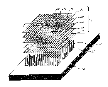
FIG. 1 is an exploded perspective view of a first
embodiment according to the present invention, while FIG. 2
is a sectional view taken on line a-a of FIG. 1.
Referring to FIG. 1, the first embodiment of the
package structure according to the present invention
comprises a plurality of tape carriers 1, a wiring board 2,
and a plurality of pins 22 vertically secured on the wiring
board 2. The pins 22 are arranged in a lattice.
2195Q38
9
Referring to FIGS. 2 and 3, each of tape carriers la -
1e comprises a base film 13, and an LSI 12 is mounted on the
base film 13. The base film 13 is formed of resin such as
polyimide, glass epoxy, polyester, or BT resin. A wiring
pattern 14 is provided on the upper surface of the base film
13. The wiring pattern 14 is formed by press fitting or
bonding copper foil. It may be possible that the wiring
pattern-14 i's formed by etching conductive foil plated on
the base film 13 into a desired pattern. A device hole is
provided at the center of the base film 13. A part of the
wiring pattern 14 projects into the device hole to form an
inner lead 15. The inner lead 15 is plated with tin (Sn),
gold (Au) (given the first coat of nickel (Ni)), or solder.
The inner lead 15 is connected to a pad of LSI 12 placed on
the device hole. For this connection, connection technique
such as gang bonding or single-point bonding is employed.
Connection of the inner lead 15 and the plane of the circuit
of LSI are encapsulated by resin 16. Epoxy or silicones can
be used as the resin 16.
Referring to FIG. 3, the tape carrier 1 is provided
with an external connection terminal 11. The external
connection terminal of the tape carrier 1 comprises a
through hole 18, and a conductive pattern 17 provided on the
inner surface of the through hole 18. The conductive
pattern 17 may be provided on the upper and bottom surfaces
2195038
of the base film 13 in addition to the inner surface of the
through hole 18. Each conductive pattern 17 is connected to
the LSI 12 through the wiring pattern 14 and the inner lead
15. The external connection terminal 11 are. aligned with
5 the pin 22 mounted on the wiring board 2, and arranged in a
lattice.
Referring to FIG. 4, the pin 22 is connected to the pad
21 on the wiring board 2 with solder 23. The pin 22 is
connected to an~inner wiring layer of the wiring board 2.
10 Referring to FIGS. 2 and 3 again, the pin 22
corresponding to the through hole 18 provided through the
external connection terminal 11 is inserted into the through
hole 18. When the conductive pattern 17 on the through hole
18 contacts the pin 22, the external connection terminal 11
is electrically connected to the pin 22. On the wiring
board 2, a plurality of tape carriers la - 1e are
sequentially laminated. In FIG. 2, the tape carriers la -
1e are laminated. The pin 22 passes through the external
connection terminals 11a - 11e of the tape carriers la - 1e.
This connects the external connection terminals lla - 11e of
the tape carriers 1a - 1e each other.
It is desirable that the corresponding external
connection terminals 11a - 11e of the tape carriers la - 1e
have common functions. Because the corresponding external
connection terminals lla - 11e are connected by the same pin
. . 219~03~
11
22. The functions of the external connection terminal 11a -
11e include to serve as a signal terminal, a power supply
terminal, and a ground terminal. When the functions of the
external connection terminals lla - 11e cannot be made
common, it is necessary to electrically connect a specific
one of the external connection terminals 11a - 11e to the
pin 22, and to insulate the remainder from the pin 22 in
question. Such insulation can be achieved by not forming
the conductive pattern 17 on the external connection
terminal 11 to be insulated. It may be also achieved by not
connecting the conductive pattern 17, formed on the external
connection terminal, 11 to the wiring pattern 14.
Referring to FIG. 5, the insulation of the external
connection terminal 11 may be achieved by applying
insulating material 41 on the conductive pattern 17.
Referring to FIG. 6, the insulation of the external
connection terminal 11 may be achieved by applying
insulating material 42 on the corresponding area on the pin
22 which is opposed to the external connection terminal 11
to be insulated. It may be allowed to apply the insulating
material 42 on the entire pin 22 followed by removing it
from an area opposing to the e::ternal connection terminal 11
required to be connected.
Referring to FIG. 7, when the tape carriers la and lc
of the tape carriers la - 1c are connected to the pin 22,
. , 219038
12
the insulating material 42 is applied on the position on the
pin 22 which opposing to the conductive pattern 7 of the
external terminal llb of the tape carrier 1b. Therefore,
the external connection terminals lla and 11c are connected
to the pin 22, and the external connection terminal 11b is
insulated from the pin 22. The approach to selectively
connect the pin 22 through application of the insulating
material onwthe pin 22 is effective when the LSI 12 is a
memory LSI. It is because the tape carriers 1 with the same
structure can be laminated.
Next is described the manufacturing method of the first
embodiment.
In a first step, the LSI 12 is mounted on the tape
carrier 1. In a second step, a plurality of tape carriers
la - 1d are sequentially laminated by inserting the pin 22
into the external connection terminals lla - 11e. In a
third step, the lower end of pin 22 is soldered to the
wiring board 2. In this method, the operation of LSI 12 is
inspected after either the first step or the second step.
It may be manufactured by the following method.
In a first step, the pin 22 .is vertically mounted on
the wiring board 2. In a second step, the LSI 12 is mounted
on the tape carrier 1. In a third step, the tape carriers 1
are sequentially laminated on the pin 22 vertically mounted
on the wiring board 2.
219~~38
13
Now, a second embodiment of the present invention is
described below.
Referring to FIG. 8, in the second embodiment, a heat
sink 31 is placed on the tape carrier la positioned on the
top of a plurality of tape carriers. The heat sink 31 is
connected on the non-circuit plane of the LSI 12 on the tape
carrier 1a. The heat sink 31 is supported on the wiring
board 2 by a support pin 33. Heat conductive resin 32 is
filled between each of the LSI 12. In the second
embodiment, heat generated from each of the LSI 12 is
transmitted to the heat sink 31 through the LSI 12 and the
heat conductive resin 32 and radiated from the heat sink 31.
Now, a third embodiment of the present invention is
described.
Referring to FIG. 9, in the third embodiment, a heat
conductive plate 34 is inserted between each of the tape
carriers 1. The head conductive plate 34 is formed of a
good heat conductive material such as copper or aluminum. A
heat sink 35 is mounted on one end of the heat conductive
plate 34. Heat generated from the LSI 12 is transmitted to
the heat sink 35 through the head conduction plate 34 and is
radiated therethrough. If it is desired to radiate much
heat, the heat conductive plate 34 may be arranged to
protrude from each side of the tape carrier 1 and mount the
heat sink 35 on each end of the heat conductive plate 34.
2195Q38
14
Now, a fourth embodiment of the present invention is
described.
In the fourth embodiment, some modification is taken
for the design of shape of the through hole 18 or the pin 22
to achieve surer connection between the pin 22 and the
external connection terminal 11.
Referring to FIG. 10, the through hole 18 is formed in
an oval.
Referring to FIG. 11, the through hole 18 is formed in
a rectangular.
Referring to FIG. 12, the pin 22 has an oval in cross
section.
Referring to FIG. 13, the pin 22 has a rectangular in
cross section.
In the fourth embodiment, insertion of the pin 22
causes the through hole 18 to be expanded and slightly
deformed. This make surer electrical connection between the
pin 22 and the external connection terminal 11.
Now, a fifth embodiment of the present invention is
described.
Referring to FIG. 14, in the fifth embodiment, the
through hole 18 has a tapered surface. This make easy
insertion of the pin 22.
Now, a sixth embodiment of the present invention is
described.
' ' 2195A38
In the sixth embodiment, some modification is taken for
the shape of the surface of the pin 22 so that the pin 22 is
difficult to be removed from the through hole 18.
Referring to FIG. 15, the pin 22 is formed to have a
5 saw-toothed surface.
Referring to FIG. 16, the pin 22 is formed to have a
waving surface.
Now, a 'seventh embodiment of the present invention is
described.
10 Referring to FIG. 18, in the seventh embodiment, the
conductive pattern 17 on the external connection terminal 11
and the pin 22 are connected by solder 24.
Next is described the manufacturing method of the
seventh embodiment.
15 Referring to FIG. 17, in a first step, the solder 24 is
plated on the surface of pin 22. Thereafter, the pin 22 is
inserted into the through hole 18.
Referring to FIG. 18, in a second step, the solder 24
is heated by reflowing. This heat melts the solder 24.
Consequently, the conductive pattern 17 and the pin 22 are
connected by the solder 24. The operation of LSI 12 is
desirable to be inspected prior to performing the second
step. It is because a defective tape carrier 1 is difficult
to be replaced after performing the second step.
219~~38
16
According to the seventh embodiment, the pin 22 is more
surely connected to the external connection terminal 11.
Now, modifications of the present invention are
described.
As the structure and method for mounting the LSI 12 on
the base film 13, those used in TAB mounting can be
employed. For example, area TAB mounting may be employed.
The area TAB mounting is effective when the LSI 12 has a
number of connection terminals.
The wiring patterns 14 may be provided on both sides of
the base film 13.
A multi-layered tape that a plurality of insulating
layers and wiring layers are alternately laminated may be
used as the base film 13. In such case, it is preferable to
separately use each wiring layer as a signal layer, a power
supply layer; and a ground layer. I,n this structure,
electrical characteristics can be improved. Thus, it
becomes possible to transmit signals at a high speed. In
addition, the packaging density can be more increased
because more complex connection such that signal lines are
three-dimensionally intersected each other can be achieved.
The wiring board 2 may be provided with a through hole
that the pin 22 is inserted thereinto. The pin 22 is
connected to the though hole in the wiring board 2 by
solder.
. 219038
17
The external connection terminals 11 and the pins 22
may asymmetrically be arranged to prevent the pins 22
inserting into the tape carriers l in error. Examples of
asymmetrical arrangement include increase or decrease the
number of external connection terminals 11 by one. This
uniquely determines the orientation of the tape carriers 1
inserted by the pins 22.
In the~structure of the second and third embodiments,
various cooling structure may be used in place of the heat
sinks 31 and 35. For example, a water-cooling unit or a.
Peltier cooling element may be used.
The entire package structure may be encapsulated in a
case instead of encapsulating individual LSIs 12 with the
resin 16. In addition, the resin 16 may be injected between
the tape carriers la - 1e after laminating them. This
allows it to protect the LSIs 12 from dirt or moisture.
Electronic components other than the LSI 12 may be
mounted on the tape carrier 1. For example, a tape carrier
1 mounted with a passive device such as a capacitor or a
resistor may be laminated together with the tape carrier 1
mounted with the LSI 12. This can stabilize the operation
of LSI 12.
Only the arrangement of e:::ernal connection terminals .
11 is required to be common for each tape carrier. For
~19~038
18
example, the arrangement, geometry or structure of the
wiring pattern 14 may vary from a tape carrier to another.
A tape carrier mounted with a microprocessor and a tape
carrier 1 mounted with a memory may be laminated. In this
case, it may be possible to place the tape carrier mounted
with the microprocessor on the uppermost layer; and to place
the tape carriers mounted with high speed memories on the
subsequent layers. The high speed memory may be used as a
cache memory.
Some of pins 22 may be not connected to the internal
conductor of the wiring board 2. Such pins 22 only have a
function for connecting the external connection terminals 11
each other.
As described above, according to the package structure
for an integrated circuit according to the present
invention, since the external connection terminals of the
tape carrier are arranged in a lattice, the number of
external connection terminals can significantly increase.
In addition, each tape carrier can be easily fabricated
by the TAB technology. Furthermore, electrical connection
can be easily achieved between the tape carriers by
inserting the conductive pins into the through hole in each
tape carrier.
Selective connection between the pins and the external
connection terminals can be easily achieved. Specifically,
2195a38
19
it is sufficient not to provide.the conductive pattern. The
conductive pattern may not be connected to wiring.
Furthermore, insulating material may be applied on the pin
or the external connection terminal. Even if there is a
non-common terminal, it is not necessary to shift the
external connection terminals. Thus, even if the number of
non-common terminals increases, the packaging efficiency is
not deteriorated.
Each integrated circuit is mounted on the tape carrier.
Thus, individual integrated circuits can be inspected before
a plurality of tape carriers are connected. Any defective
integrated circuit can be discarded by tape carrier.
While this invention has been described in conjunction
with the preferred embodiments thereof, it will now readily
be possible for those skilled in the art to put this
invention into practice in various other manners.