Note: Descriptions are shown in the official language in which they were submitted.
WO 96!03808 PCT/CA95/00432
- 1 -
DIGITAL PHASE LOCKED LOOP
This invention relates to a phase locked loop, and
in particular to a digital phase locked loop capable of
recovering a clock signal from one or more input signals
subject to fitter.
In digital networking applications, there is a
requirement to provide timing references to interface
circuits to T1 and E1 (see EPT) primary rate digital -
transmission links. These timing signals must meet
ACCDNET R T1.5 and ETS1 ETS 300 01111 specifications for
a 1.544 MHz (T1) or 2.048 MHz (CEPT) input reference.
These specifications impose strict requirements on fitter
and stability.
The common method of providing such timing signals
is to use a phase locked loop. Typically, this consists
of a phase detector comparing the input signals with the
output of the loop divided by a suitable factor, a loop
filter to eliminate high frequency fluctuations, and a
controlled oscillator whose frequency is controlled in
such a way as to eliminate the phase difference detected
by the phase detector.
It has long been known to employ a VCO (voltage
controlled oscillator) as the controlled oscillator in
the loop. U.S. Patent No. 4,577,163 discloses a phase
locked loop in which the VCO is replaced by a DCO
(digital controlled oscillator) whose output is divided
by a factor K and fed back to the phase detector. In the
patent, the DCO is clocked by a clock signal F~i~k- Since
2~1~~193
_ 2 _
the DCO cannot respond to phase shifts less than one
clock cycle, Fclk is the limiting factor for accuracy in
this type of phase locked loop. In order to meet ACCUNET
specs, a local oscillator having a frequency of 200 MHz
or more must be employed.
Such high frequency local oscillators are expensive,
energy-consuming, and prone to the emission of
electromagnetic interference (EMI).
U.S. Patent No. 5,218,319 discloses a phase locked
loop in which a local oscillator feeds a tapped delay
line. The output signal is taken from one of the taps of
the delay line according to a phase comparison effected
with the input signal. The problem with this arrangement
is that it provides no fitter suppression for the
reference signals. As a practical matter, due to the
inherent properties of the transmission medium, incoming
T1 and El signals will be subject to fitter, and this
must be substantially suppressed in order to meet the
ACCUNET specifications.
European patent specification EP 0299724 discloses a
digital phase-locked loop for recovering a stable clock
signal from at least one input signal designed for use in
a digital television. A variable delay line is included
to eliminate distortion arising drift in the
synchronizing signal. This device, however, is not
designed for the telecommunications environment and is
not capable of meeting the rigid fitter requirements of
the ACCUNET specifications with an inexpensive, low-
frequency local oscillator.
An object of the invention is to provide a phase
locked loop that alleviates the aforementioned problems
with the prior art.
Accordingly the present invention provides a digital
phzse lccked loop for recovering a stable clock signal
ptVIEND~D S~~ET
iP ~PJEP
295193
from at least one input signal subject to fitter,
comprising a digital input circuit receiving said at
least one input signal; a digital controlled oscillator
for generating an output signal at a desired frequency
and a control signal representing a timing error in said
output signal; a stable local oscillator for providing
clock signals to said digital controlled oscillator;
tapped delay line means for receiving the output signal
of said digital controlled oscillator, said tapped delay
line means comprising a plurality of buffers each
introducing a delay of less than one clock cycle of said
digital controlled oscillator, said tapped delay line
means producing an output signal from a tap determined by
said control signal; and a digital phase comparator for
receiving said at least one input signal from said input
circuit and said output signal from said tapped delay
line means to generate a digital input signal controlling
said digital controlled oscillator, characterized in that
said tapped delay line means comprises a pair of
20.. interlaced tapped lines to permit the generation of a
.frequency at twice the output frequency of the digital
controlled oscillator.
In accordance with the invention, due to the
combination of DCO and tapped delay line, the local
oscillator can be of low frequency, for example 20 MHz.
Typical unfiltered intrinsic output fitter is 0.04 UI
(Unit Interval) peak-to-peak with fitter attenuation of
15 dB at 10 Hz, 34 dB at 100 Hz and 50 dB at 5 to 40 kHz.
The DCO thus provides a very stable output determined by
the stability of the local oscillator. Low power 20_ MHz
oscillators are conveniently available.
Since the DCO directly controls the tapped delay
line, fitter free precision can be maintained to a
fraction of a clock cycle.
AMENDED S~EFT
i!'~AJEP
219 5 i 9 3 PCTlCA95/00432
wo mo3so8
- 4 -
In a preferred embodiment, the digital controlled
oscillator is an adding type rate multiplier whose carry
signal generates the output signal when an overflow
condition is attained. The remainder term indicates the
timing error and is used to generate the control signal
for selecting the appropriate tap.
The regenerated clock signal can also be used to
control the input circuitry and thus give better fitter
performance _
In some applications, two or more input reference
signals may be supplied, with the phase locked loop being
_ switchable between the input signals. In order to
prevent discontinuities on switchover, the input circuit
continually monitors the phase difference between the.
active and inactive reference inputs. A virtual
reference signal is created With a constant phase
difference relative to said input signals, so that on
switchover no discontinuity arises.
The invention also provides a method of recovering a
stable clock signal from at least one input signal
subject to fitter, comprising the steps of generating
local clock signals with a stable oscillator; clocking a
digital controlled oscillator with said local clock
signals; feeding a first output of said digital
controlled oscillator to a tapped delay line; controlling
said tapped delay line with a second output of said
digital controlled oscillator representive of a timing
error in said first output to generate clock signals
PGTICA95/00432
WO 96103808
- 5 -
having a precision greater than one clock cycle of said
stable oscillator; and controlling said digital
controlled oscillator with a digital phase comparator
that compares the output thereof with said at least one
input signal.
The invention will now be described in more detail,
by way of example only, with reference to the
accompanying drawings, in which:-
Figure 1 is a block diagram of a prior art phase
locked loop;
Figure 2 is a block diagram of a phase locked loop
in accordance with the invention;
Figure 3 is a block diagram of a DCO employed in the
invention;
Figure 4 shows the phase deviation of the DCO
output;
Figure 5 is a block diagram of the phase detector;
Figure 6 shows the phase difference measured with an
interpolation counter;
Figure 7 is a timing chart showing the reference
signals; and
Figure 8 is a timing chart showing the operation of
the delay lines.
WO 96/03808 PCT/CA95/00432
- 6 -
Referring now to Figure 1, a standard phase locked
loop comprises a phase detector 1 receiving a reference
signal in, a loop filter 2, a controlled oscillator 3,
which is conventionally a voltage controlled oscillator,
and a divider circuit 4 generating a feed back signal for .
the second input of the phase detector 1. The function
of the loop filter 2 is to eliminate high frequency
fluctuations in the control signal.
The phase detector 1 ensures that the controlled
oscillator 3 generates an output in synchronism with the
input signal in.
Such a conventional phase locked loop does not
provide adequate means for eliminating fitter in the
input signal in, such as is present on a T1 or E3 link.
Also, even if the controlled oscillator 3 is a digital
controlled oscillator, the circuit cannot meet the
technical specifications for T1 and E1 links unless the
clock frequency of the oscillator clocking the digital
controlled oscillator 3 is very high (in the order of 200
MHz or more).
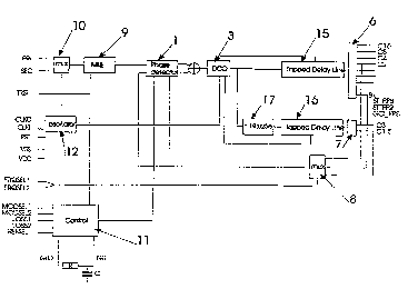
Referring now to Figure 2, the phase locked loop in
accordance with the invention comprises a digital phase
detector 1, a digital controlled oscillator 3 feeding
respective tapped delay lines 15, 16, actually each
consisting of a pair of interlaced tapped delay lines,
connected to output circuits 6, 7 and providing a range
of clock signals at different frequencies respectively
for E1 and T1 circuits. The output circuits 6, 7 are
2~9519~
connected through multiplexor 8 to one of the inputs of
phase detector 1. The other input is connected to MTIE
circuit 9, whose function will be described in more
detail below, receiving the output of muitiplexor 10
receiving primary and secondary inputs PRI, SEC. PRI and
SEC can, for example, be first and second incoming T1
links from which it is desired to generate timing signals
for the local interface circuits.
Control unit 11 acts as a state machine controlling
the operation of the device. Oscillator 12 is a stable
MHz crystal oscillator with nominal 50 nanosecond
cycle duration. Unit 17 multiplies the output of the DCO
3 by 193/256 to generate timing signals for a Tl
interface.
15 The DCO 3 is shown in more detail in Figure 3. It
comprises an adding rate multiplier that generates the
desired output frequency. An input word (DCOin) is fed to
adder 20, whose least significant section is BCD (binary
coded decimal) and most significant portion HEX coded for
20 reasons to be explained. The DCO 3 is clocked by the 20
MHz clock signal from stable oscillator 12. As the input
word DCOin is repeatedly added to the initial value of the
adder P, the adder periodically~overflows, and the
resulting carry signals constitute.-f.he output signal of
the DCO 3. If there is a remainder term at the time of
overfloh~, this appears in register 23 and represents the
timing error of the DCO output (Figure 8). This
remainder term (restterm) is used to control the tapped
delay line in a manner to be described below.
AMENDED Si IEET
1P~PJEP
2195~~3
_8_
The DCO 3 generates a main frequency of 16.384 MHz
for El and 12.352 MHz for Tl. The frequency generated by
the DCO is given by the equation:
Fgen = _P x f ~loc~c / 2
S Q
where Q is the capacity of the adder, P is the initial
value of the adder (P is less than Q) and f~lo~x equals the
- clock frequency of the DCO 3.
As the DCO operates on a clock frequency of 20 Mhz,
in accordance with the Shannon theorem, the maximum
frequency that can be generated is lOmhz, i.e. the sample
frequency divided by two. This is apparent from Figure
8, which shows that the DCO changes state on the leading
edges of the clock pulses. However, by replacing every
edge in the DCO output with a 25ns pulse, the DCO output
frequency is doubled. This signal (16.384 or 12.352mhz)
is adjusted in phase by the two interlaced delay lines in
each of tapped delay lines 15, 16 (Figure 2). The output
sum has thus has double the frequency Of Fgen-
In typical telecommunications applications, the
center frequencies generated by the DCO 3 should be
multiples of 8000 Hz, the standard frame frequency.
Thus, Q must have for a divisor at least 20,000,000
divided by 8000, which equals 2500, (or in other words 2Q
- Pf~lock~fgen 1 . Since P must be an integer, Q must be a
multiple of 2500. This result can be achieved by
employing a mixed coding scheme, which in the preferred
embodiment comprises BCD and Hex as described above.
AMENDED S. SET
IPEA/EP
2195193
- 9 -
The value for P required to generate a given
frequency is indicated in Table 1 below. For a frequency
Faer of 8.192 Mhz, according to the formula above P must
equal 2,097,152 dec. This value is coded in a mixed
representation, which is a combined BCD/hex
representation in the example. The combined values of
the interpolation and cycle slip counters must also be
encoded in this representation before they can be added
to the value of P for the DCO 3.
The resolution of the DCO 3 is determined by the
value of Q, which for one practical embodiment is 2.56 x
lOs, and thus the resolution is 0.5 x 1 over 2560000 X 20
MHz = 3.9 Hz. The resolution for the generated frequency
is only as good as the ratio between the set number P and
the least significant bit. Since this ratio is
1/2097152, the relative accuracy is therefore 0.48 parts
per million.
TABLE 1
value P fgen resolution
@ Q = 2,560,000
(around
and center)
f~lo~x=20, OOOMHz
2,097,152 (dec) 8.192 MHz 3.9 Hz
D1(hex) 7152(dec) 0.48 ppm
AMENDED S~EE~
r y_y ~ L
WO 96103808 PGTlCA95/00432
- 10 -
Thus, the highest frequency that is generated by the
DCO, 16.384 MHz, has a resolution of 7.8 Hz with an
accuracy of 0.48 parts per million_
Figure 4 shows the output of the DCO 3. This is
delayed by a timing error t~n indicated by the remainder
term in register 21. As indicated above, the output of
the DCO 3 is fed to tapped delay line pairs 15, 16. Each
delay line consists of a number of buffers with a total
delay of one DCO clock cycle. When the DCO signal is fed
through the delay lines and taken from a given tap, the
edge in the DCO signal will be somewhere between the two
edges of the DCO clock.
The point Where the signal has to be tapped from the
delay line is determined by the remainder term of the DCO
3 when it generates an edge. The remainder term
indicates the delay in generation of the edge. The
smaller the remainder the more timely the edge
generation. This can be seen from the following simple
illustration. If the adder capacity is 8, and the word
added is 4, each time adder overflows there will be a
remainder of zero, indicating the carry pulse is on time.
However, if, for example, the added term is 3, the adder
will overflow prematurely, i.e. when there is a remainder
of 1 in the register, and this remainder thus represents
the timing error.
When the adder in the DCO reaches an overflow
condition, the carry toggles the output signal, and thus
generates an edge in the DCO output signal fg~n. The
~19.~19~
- 11 -
capacitance Q of the DCO represents one cycle of the
system clock on which the DCO runs. When the DCO 3 has a
remainder term when an edge fgen is generated, the term R
represents the time error tern which is a fraction of the
clock period tclocx of the system clock.
terr = R tclocx
P
~ In Figure 4, the output and remainder term of a DCO
with Q=10 is shown. With P=8, the DCO generates a
frequency of 9/5 system clock. It can easily see be seen
that the frequency of the DCO output signal is correct,
but the edges are too late. The larger the remainder
term, the later the edge. The first edge has a remainder
term of 6. This means that the edge is 6/8=0.75 clock
cycle too late. When the remainder term is 0, the edge
is right on time.
The edge from the DCO 3 has to be advanced in time
by the term terr in the formula above. This is achieved
by delaying the edge with tdei. the complement Of terr~
tdel = ~3 - R/P) tclock
The delay calculation uses the assumption that a
certain number of delay element s "fits" in one clock
cycle. However, over temperature, voltage and process
variations this is very irregular. Therefore the delay
line provides a length that is suited for worst case
conditions according to the process of implementation.
Also a measurement is performed to calculate the number
of delay elements that fits in a single system clock
AMENDED S!~-IEFT
~r'~ r~i:=~
._ ,
2195i9~
- 12 --
cycle. For this reason the delay line elements are
connected to the D inputs of D-flip-flops, with a clock
driven by the system clock. By measuring the place where
the significant 0/1 transition in the sampled delay line
occurs (with a priority encoder), the number of elements
in one complete system clock cycle is determined. This
number is combined with the remainder term to calculate
the precise tap that should be used.
The remainder term provided by the DCO 3 is much
larger than the tapped delay can cope with; by using 7
bits of the remainder term the accuracy is sufficient for
driving a tapped delay line with 69 taps (7 bits would
normally correspond to 128 taps, but one bit is lost in
the caicuiation process. The number of taps guarantees
sufficient phase accuracy over the full temperature and
voltage range while the size of the circuitry remains
acceptable.
The outputs of the DCO 3 consist of a clock signal
(basically 8.192 MHz) and a remainder term. The
remainder term is used directly for the driving of the
tapped delay line 15, 16, as explained above. The tapped
delay line pair 15 generates a 16.384 MHz clock and this
clock drives dividors 6 to generate the C8, C4, C2,
GCI FP8, ST FPS and ST-FP2 signals.
The DCO can be extended with, for instance, 9 bits
extra on the adder stage. The added 9 bits will always
indicate a number of whole cycles that are generated by
the original DCO. If one takes the contents of the whole
plV?FNC~~ S~FFT
t~_:,,~ _~,
219519
- 13 -
DCO plus extension and performs the multiplication
193/256, the number that results can be used for accurate
generation of a frequency which is 193/256 8.192 MHz =
6.176 MHz. This frequency is in turn used to generate a
frequency of 12.352 MHz required for T1 circuits.
The multiplication by 193 is performed using shift
and add functions: 193 equals 128+64+1. This however is
only done for the few bits that have significance on the
output. The lower bits of the DCO are not of interest
since the accuracy of the delay lines for both T1 and El
demand limited phase accuracy. (The DCO itself is of
course very long since there not only the phase accuracy
has a minimal quality, but also the frequency: this adds
extra bits). The most significant bits that would result
from the multiplication are of no interest since they
represent whole cycles.
A last element on the indirect frequency synthesizer
is the means to align the 8 kHz pulse with the T1 clock.
The El clocks and the 8 kHz pulses are hard linked and
always have the correct phase relation. However the
divided T1 clock of 1.544 MHz may not automatically come
to the correct phase relation of the 8 kHz since the
divisor of 12.352 MHz to 1.544 MHz is never forced to do
so. This problem is solved with a reset circuit on the
Tl divisors driven by the 8 kHz pulse. This resetting
never has any asynchronicity problems since the Tl is,
through the 193/256 operation, hard linked to the E1
clocks.
AMENDED S~EFT
IPFG lPP
pGT/CA95/00432
wo 96ro3sos 219 5 I 9 3
- 14 -
The phase detector 1 will now be described in more
detail with reference to Figures 5 and 6. As shown in
Figure 5, this comprises an up/down counter 30, adder 31
and programmable adder/subtractor 32.
The phase difference for two 8 kHz references is
shown in Figure 6. The phase error is considered of
consisting of two parts, an absolute part, and a relative
part. The absolute part is a measure of the phase
relationship between the two frequencies over one cycle,
and the relative part keeps track of cycle slips between
the two frequencies. The absolute measurement is
straightforward and uses the same configuration whether
' the reference is 8 kHz, 1.544 MHz, or 2.048 MHz.
A number of 16.384 MHz cycles (for E1, 12,352 for
T1) in the measurement interval is typically even, so the
result of the measurement is typically even. However,
due to the sampling of the reference frequency with a
clock that is following the reference, the measurement
interval varies with ~ 1 clock cycle and may become an
odd number of clock cycles. This ensures that the LSB of
the measurement is not fixed and therefore the accuracy
of the measurement is increased. Due to the absolute
measuring method with an up/down counter, half an 8 kHz
cycle phase difference comes out of the absolute
measurement as 2048 cycles (whereas 62.5 us is 1024 clock
cycles of 16.384 MHz).
The relative measurement is more variable and uses
an equivalent value for each cycle slip that occurs: A
WO 96/03808 PCT/CA95/00432
- 15 -
cycle slip of 8 kHz is identical to 2048, but must match
if concatenated to the absolute measurement. The same
holds for measurement of the 2.048 Ngiz reference. Thus
the relative measurement counts 4096 or 16 for every
cycle slip, depending on selection of 8 kHz or 2.048 MHz
as reference.
If the selected reference is 1.544 MHz, the settings
for relative and absolute counters are precisely the same
as the settings for 2.048 MHz. Only the counting
frequency used in the counters is reduced to the 12_352
regenerated frequency. This has only bearing upon the
low pass frequency, which is lowered with a factor
193/256 ~ 0.75.
The absolute and relative measurements are combined
with a simple adder 31.
The basic arrangement used for a low pass filter
included in phase detector 1 is quite straightforward.
The counter 30 measures the.actual phase error, the phase
error is taken over (sampled) as a frequency offset in
the DCO. The DCO integrates this offset value for the
next sample period and thus reduces the measured phase
error.
It should be noted that the frequency offset
resulting from the measurement is very small. In the
next sample period the error will only be canceled for a
minor part. This attenuation type of mapping combines
with the sampling rate to form an effective low pass
frequency of a few Hz .
PCT/CA95I00432
WO 96103808
- 16 -
Since the error is reduced a bit in the next
sampling period, the next time the "repair" of the error
will become slightly smaller. It can be calculated that .
the error repair curve closely mimics a first order low
pass function, which happens to be the function that we ,
would like to achieve. The quality of the curve is set
with the ratio between sampling rate and effective low
pass frequency (which precisely.equals the attenuation).
In this configuration this means that with 8000 Hz
sampling and effective iow pass of 2 Hz, the first order
is approached with at least more than 60 dB quality.
This is important since this maps to a worst case
transfer outside the pass band of 60 dB, which is better
than the ACCUNET spec. This approach is very crude and
can be refined quite easily.
The effective low pass frequency can be calculated
from the frequency offset generated from a given phase
error. In a first order system the tangent of the output
at the beginning of the step response hits the 100s input
value mark precisely after T seconds. This i results in a
certain low pass frequency.
The references used for the phase measurement always
have a maximum fitter frequency content according to the
Shannon theorem; an 8 kHz square wave signal never
carries fitter above 4 kHz. In turn a 2.048 MHz
reference carries fitter up to a maximum of 1.024 MHz.
If a reference is divided the maximum fitter frequency
goes along with it, folding all higher components into
the next maximum fitter band. As such a 2.048 MHz signal
WO 96103808 PCT~CA95~04432
- 17 -
with 32 kHz fitter, divided to 8 kHz, folds the 32 kHz
fitter into the DC range. Since the PLL passes DC fitter
undisturbed the folded fitter is not suppressed, which
violates the ACCONET specs. Thus the frequency used for
phase measurement must always be the maximum available
without division.
If a higher reference frequency is used, but the
counters keep running on the same counting frequency, the
low pass frequency does not change, but the quality of
the first order low pass function increases. With a
reference frequency of 2.048 MHz and a low pass of 2 Hz
this means theoretical stop band performance of -120 dB.
This effect is used in he sense that no matter whether
the input reference is 8 kHz, 1.544 MHZ or 2.048 MHz, the
same phase detector is used, without major modifications.
The MTIE circuit 9 will now be described in more
detail With reference to Figure 7, which shows the
primary and secondary PRI, SEC, input signals to the
multiplexor circuit~l0. The MTIE circuit 9 creates a
virtual reference, which has a constant phase
relationship to the primary reference PRI. The phase
difference can in fact be zero, so that the virtual
reference is in phase with the primary reference,
although the actual phase difference is not important.
The secondary reference SEC is phase shifted by an amount
0~, which is continually monitored.
The secondary reference is delayed by an amount
equal to ~~ so as to bring the delayed secondary
wo 96ro3808 2 '~ E~ ~ ~ ~ ~ PCT/CA95I00432
- 38 -
reference into phase with the virtual reference. Thus,
when it becomes necessary to change over references due
to degradation of the primary reference, no phase jump is
observed since the phase derived from the secondary
reference is maintained in phase with the previous
reference derived from the primary reference.
The shift amount is determined before the switch
over takes place by measuring the phase distance between
the current virtual reference and the not yet selected
reference.
An important feature is the use of the regenerated
16.384 MHz clock as a sampling clock_ If the 20 MHz
clock were used, sampling inaccuracy in the steady state
would result, and this would introduce low frequency
drifts relative to the reference with a maximum value of
50 ns. Though this is acceptable according to the
specifications, the better performance is preferred.
Each time a measurement is completed the result is
stored in a register. Upon switchover, the measured
value can be used to drive a counter which generates the
phase shift of the new reference. In this counter the
new reference is used to start the counter and generate a
new reference pulse at the 0 position. A detail in this
process is that if a new reference pulse is detected and
the counter has not reached the 0 position yet, the
virtual reference is generated just the same while
starting a new count cycle; if this mechanism were not be
present cycle slips might occur.
WO 96J03808 PGT/CA95/00432
- 19 -
The switchover from one reference to another is
guarded. After selection of the new reference input, the
circuit waits for three periods of the virtual reference
before it can switch back to the previous reference
signal. This is maximum the settling time of the
mechanism that measures the phase difference between the
to-be-used reference and the current virtual reference.
Fast switching between references inputs can therefore
not disrupt the functioning of the MTIE circuit 9.
The MTIE circuit 9 behaves identically for T1, E1
and 8 kHz references.
The MTIE circuit 9 thus samples the reference clocks
and determines the phase relation between the not used
external and the used external reference. The phase
relation is stored as a simple countervalue. Upon a
rearrangement the value is used to delay the new
references edges to a more correct position in the MTIE
sense. This is done by a simple loadable down counter.
If the down counter after rearrangement reaches the
0 position, the internal reference signal VIR (Virtual
Internal reference) is given. Upon a new detection of an
edge on the external reference the counter starts again
to count down. If the counter has not reached 0 yet, but
an external reference edge is already detected (which
basically is too early and points to fitter, small or
large) the counter is directly reset to start counting
again, while a VIR is given. This is acceptable; this way
WO 96103808 PGT~CA95/00432
- 20 -
the MTIE circuit just seems to pass the fitter, which is
of course allowable.
The described phase locked loop can be used for
synchronization and timing control for T1 and CEPT
digital transmission links, ST bus clock and frame pulse
sources, and primary trunk rate converters, for example.
In addition to providing synchronized PLL outputs at
2.048, 1.544 MHz, or 8 kHz primary rate, the PLL can also
provide additional high speed output clocks at rates of
3.088 MHz, 4.096 MHz, 8.192 MHz, and 16.384 MHz for back
frame synchronization. Also the device can De used ~u
conjunction with an analog phase locked loop to generate
2 Mhz, or 155 Mhz signals for ATM, for example.
The phase locked loop has four modes of operation,
namely normal and manual mode, holdover mode, freerun
mode, and automatic mode.
In manual mode operation, the input reference
selection is accomplished using a 2-to-1 multiplexer,
with the RSEL pin providing selection control. As shown
in Table 2, for MANUAL mode operation RSEL=0 selects PRI
as the primary reference input, while RSEL=1 selects SEC
as the primary reference input.
21~5~9~
WO 96/03808 PCT/CA95100432
."~.,.
- 21 -
Table 2
Mode RSEL Reference Input
Selected
S Manual 0 PRI
Manual 1 SEC
Automatic 0 state machine control
Automatic 1 state machine control,
but treats SEC as primary
and PRi as secondary
There are three possible input frequencies for
selection as the primary reference clock. These are 8
kHz, 1.544 MHz, and 2.x48 MHz. Frequency selection is
controlled by the logic levels of FSEL1 and FSEL2, as
shown in Table 3. This variety of input frequencies was
chosen to allow the generation of all the necessary T1
and E1 clocks from either a T1, E1 or frame pulse
reference source.
TABLE 3
FSEL FSEL Input Reference Frequency
2 1
0 0 Reserved
0 1 8 kH2
1 0 1.544 MHz
1 1 2.048 MHz
In normal AUTOMATIC mode operation, the REFSEL input
tFig. 2) is set to 0 to allow the STATE MACHINE to select
the reference input based on the state of the LOSS1 and
LOSS2 inputs. If the PRI reference signal is lost
(LOSS1+HIGH, LOSS2+LOW), then the PLL enters HOLDOVER
mode immediately and stays there fore a predetermined
219519
wo 96~o~go8 rcncA9srooa32
- 22 -
time as controlled by the RC time constant connected to
the Guard Time input (GTi, GTo).
After the guard time has been exceeded, the
reference will be switched to SEC if the primary
reference continues to remain lost. The time constant
determined by the RC circuit connected to the GTi input
provides the hysteresis on automatic switching between
PRI and SEC during very short interruptions on the
primary reference signal. The Guard Time, tgt, can be
predicted using the step response of an RC network. The
capacitor voltage on the RC circuit is described by an
exponential curve. When the capacitor voltage reaches
the positive going threshold of GTi a logic HIGH level
results. This causes the state machine to move from the
holdover state of PRI to the state of using SEC as the
input reference. A logarithmic equation that can be used
for prediction of the Guard Time tgt, is given by:
The STATE MACHINE 11 continues to monitor the LOSS1
input and switches back the reference to PRI once the
primary reference becomes functional as indicated by the
LOSS1 input. A logic level HIGH on both the LOSS1 or
LOSS2 inputs indicates that none of the external
references are available. Under these circumstances, the
phase locked loop will be switched into the HOLDOVER
STATE (within a specified rate of frame slip) until a
fully functional reference input is available.
The holdover option of the phase locked loop
provides the user with the capability of maintaining the
WO 96103808 PCT/CA95/00432
- 23 -
integrity of output signals when the input reference
signals are lost. Holdover performance specified as the
rate of slip {i.e. amount of slip on 60 seconds) of the 8
kHz reference input. For both the T1 and E1 outputs the
rate of slip was measured as a function of the input
referenceJfrequency. The results measured over an
observation period of 60 seconds, are presented in Table
4.
TABLE 4
Reference Input ~ of Frame Pulse Slip
Frequency
8kHz 8~
1.544Mhz 580
2.048HZ 580
As indicated, the phase locked loop uses its own
generated frequency for sampling in data on the reference
inputs. The reason for doing so is that this achieves
synchronous sampling, giving best performance for
intrinsic jitter_ If the 20 MHz clock were used the
accuracy would fall, especially on the low frequency
wander aspect.
The circuit is truly asynchronous to the outside
world, but also asynchronous on its internals. The points
where the major blocks of the circuit interface in an
asynchronous way are all sampled with a D-flip-flop to
cover this.
Basically it detects edges on incoming signals and
decides for two counters whether to count up or down and,
WO 96/03808 PCT/CA95/00432
- 24 -
in the case of the inter counter, when to reset. The
problem lies in the relation of the two elements.
At the detection of an edge of the reference input
the inter counter, wh~.ch interpolates within one
reference cycle, is taken over into a register and reset.
At the same moment a signal is given to an arithmetic
logic unit (ALU) that this value is available and can be
sampled over (sampling is necessary here since the phase
detectors must run on the c1k1612, but the DCO and the
ALU must run on the 20 Ngiz clock. The signal REGEN-B is
used for this signaling.
The slip counter is triggered for up and down
counting by either the reference edges (up, thus driving
the DCO to higher output frequency) or the internal edges
(down). If both edges are seen at the same time no
counting is done.
The inter counter starts counting up from its reset
point, until a negative edge on the internal feedback
signal makes the counter turn over~to the negative range.
Upon detection of the edge the counter is kept silent for
one period. This is necessary to make sure that the phase
detection of a signal with itself would make the phase
detection perfect; then the result is 0 (electronically
spoken this is to balance the reset phase of the inter
counter).
The result of the process of the inter counter can
be positive or negative, and largely depends on the
precise place of the edges. If the edges change from one
PCT/CA95/00432
WO 96103808
- 25 -
measurement to another such that the value of the inter
counter swings from very negative to very positive (or
vice versa), the slip counter must indicate a slip, thus
reducing the large swing. (In coding terms; the coding
must be strictly monotone).
The operation of the inter counter places the edges
for a slip around the edge where the reference itself has
its edge. However, a slip has its effect on the inter
counter not at the moment that it occurs, but one
measurement cycle later. Thus a cycle slip must be
delayed till the next measurement. This is done by
delaying the loading of the register of the slip counter,.
so that it is not taken over-directly by the DCO, but one
measurement cycle later.
The performance of the whole circuit largely depends
on the granularity of the tapped delay. Since the circuit
must operate over all temperature ranges, process and
voltage variations (mil spec) the nominal, best case and
worst case delays are important.
From the LSI LCA300K databook it can be concluded
that the Kp (process variation),'x (voltage variation)
and Kt (temperature variation) parameters for the chip
are:
Best case: 0.7 - 0.87 - 0.83 = 0.50547
Worst case: 1.4 - 1.13 - 1.15 = 1.8193
The tapped delay line is built with one sampling
circuit for measurement of the number of taps in one
219 519 3 rcrrc~sroo432
wo 96ro3sos
- 26 -
clock cycle, two actual delay lines and a number of
tristate busses that are driven from these lines. The use
of two lines is permits switch over from one tap to
another without running into dangerous timing problems.
~ One delay line receives a pulse which is tapped with one .
tap, while the other tap is fully 0, but is being
switched from one tap to another.
If no pulse at all is passed, no tristate buffer is
active. in order to keep the bus to a fixed value the bus
is pulled down actively by extra tristate buffers (with 0
on the data input).
The tristate buffers do not have the driving
strength for 64 buffers on one line, so they are bundled
in groups of 16 and OR-ed together.
The E1 dividers take the generated 16 MHz clock and
divide it to the right frequencies, including the FP2 and
FP8 pulses. The reset is the only asynchronous details.
Since the rest of the circuit is also resetted this never
gives problems.
The T1 divider circuits take the ChKl2 clock (from
the tapped delay) and divide it to the right frequency.
However, there is one problem in this in the form of the
phase relation between E1, T1, and the FP8 pulse. The T1
circuit is reset around the FP8 pulses to ensure the
correct phase relationship. However, this is never the
case for a once reset T1 phase should always be in the
correct phase position at the place where the reset
occurs; the reset then is at the right moment and does
PCT/CA95100d32
WO 96103808
- 27 -
not make any difference in the sense that the T1 dividers
would have to come to the same positions without the
reset.
All counters and adders can be built with
primitives. Counters are based on ripple effects With
NAND/NOR sequences for the ripple stage so that delays
remain quite minimal.
The described phase locked loop thus provides an
inexpensive method of recovering clock signals, for
example in an E1 or T1 environment, that meets Accunet
specifications. The phase locked loop particularly lends
itself to large scale integration into a single chip.