Note: Descriptions are shown in the official language in which they were submitted.
INTRODUCING PROCESSING DELAY AS A MULTIPLE OF THE TIME
SLOT DURATION
Field of The Invention
The present invention relates to the field of wireless communication and more
particularly to burst mode digital wireless communication systems.
Background of The Invention
In wireless communication systems, the use of antenna arrays at the base
station
has been shown to increase both range, through increased gain, and capacity,
through
interference suppression. With adaptive antenna arrays, the signals received
by multiple
antenna elements are weighted and combined to improve system performance,
e.g., by
maximizing the desired receive signal power and/or suppressing interference.
The
performance of an adaptive antenna array increases dramatically with the
number of
antennas. Referring to an article entitled, "The Impact of Antenna Diversity
on the
Capacity of Wireless Communication Systems," by J. H. Winters, R. D. Gitlin
and J.
Salz, in IEEE Trans. on Communications, April 1994, it is shown that using an
M
element antenna array with optimum combining of the received signals can
eliminate N
<_ M I interferers and achieve an M N fold diversity gain against multipath
fading,
resulting in increased range.
Most base stations today, however, utilize only two receive antennas with
suboptimum processing, e.g., selection diversity where the antenna having the
larger
signal power is selected for reception and processing. It is desirable to be
able to
modify existing base stations to accommodate larger arrays of antennas and/or
improved received signal combining techniques. However, modifying existing
equipment is difficult, time consuming, and costly, in particular since
equipment
currently in the field is from a variety of vendors.
One alternative is to utilize an applique, which is an outboard signal
processing
box, interposed between the current base antennas and the input to the base
station,
which adaptively weights and combines the received signals fed to the base
station,
optionally utilizing additional antennas. FIG. 1 shows a base station
utilizing an
_ z ~ ~5~$~
2
applique. A key to the viability of utilizing the applique approach is that it
should
require little, if any, modification of the base station equipment. This
constraint implies
that the processing performed by the applique must be transparent to the
existing
equipment. Ideally, the signal emerging from the applique should appear to the
existing
S base station as a high-quality received signal from a single antenna.
A difficulty in obtaining transparency to the existing equipment is the delay
introduced by the signal processing performed in the applique: data
acquisition, weight
calculation, and received signal combining all introduce significant delay.
Although
typical cellular base station receivers are capable of accommodating some
delay due to
signal propagation, such delays are typically limited to the order of tens of
microseconds, whereas the delay typically required to determine the weights
for
optimum array combining is many times that. Therefore, because of the applique
delay,
the signal seen by the existing base station receiver would appear to have had
a
propagation delay far in excess of the base station's ability to compensate,
and the
system would not operate.
A previously proposed solution is to use RF analog weighting and combining of
the received signals, rather than digital signal processing of the received
signals.
However, although RF analog weighting introduces negligible processing delay
into the
signal path through the applique, the processing time required to calculate
the weights is
not negligible. The delay to calculate the weights is undesirable because a
degraded
signal will be output during the time prior to computation of the weights and
the array
performance will be poor when the fading rate is faster than a few Hz, which
is the case
at typical vehicle speeds in mobile communications.
Summa~r of The Invention
In accordance with the present invention, there is provided an apparatus for
performance improvement of a burst mode digital wireless receiver. The
apparatus
comprises a processing circuit for processing a plurality of received signals
and
providing a processed signal and a delay circuit for introducing a
predetermined delay to
the processed signal. The delay circuit is coupled to the processing circuit.
The
CA 02195489 2000-07-19
3
predetermined delay is such that the processed signal is delayed to correspond
with a
later data burst.
In a further enhancement of the present invention output signals from a
plurality of antennas provide the plurality of received signals to the
processing
circuit.
In yet a further enhancement of the present invention the processing circuit
weights and combines the received signals, where the processing circuit
reduces a
mean squared error of an output signal.
In yet a further enhancement of the present invention the processed signal
arrives at the receiver coincident with a time interval for a next data burst.
In yet a further enhancement of the present invention the processing circuit
weights and combines the received signals using a predetermined symbol pattern
within a sync sequence within a time slot.
A method in accordance with the present invention for performance
improvement of a burst mode digital wireless receiver is also described.
Brief Description of The Drawings
A more complete understanding of the present invention may be obtained
from consideration of the following description in conjunction with the
drawings in
which:
FIG. 1 is a block diagram of an adaptive array using multiple antennas;
FIG. 2 is a block diagram of a current base station with applique;
FIG. 3 shows a detailed block diagram of the applique;
FIG. 4A and 4B show the frame and time slot architecture of the uplink
digital traffic channel used in IS-136;
FIG. 5 is a block diagram of an experiment used to test the effects of
applique
delay; and
FIG. 6 is shown a flow chart of the present invention for performance
improvement of a burst mode digital wireless receiver.
Detailed Description of Various Illustrative Embodiments
Although the present invention is particularly well suited for use in TDMA
mobile radio systems and shall be described with respect to this application,
the
methods and apparatus disclosed here can be applied to other burst mode
wireless
communication systems.
_ 2~954g~
4
In TDMA mobile radio systems, such as IS-i 36, in the uplink from mobile
station to base station, data is transmitted periodically in time slots or
bursts of a known
and fixed duration. Each data burst is processed, essentially independently of
other data
bursts, by the base station receiver. Thus, it is possible to design the
applique so that it
introduces artificial delay in excess of its true signal processing delay, so
that the total
delay through the applique is nominally a multiple of the time slot duration.
With this
arrangement, the delayed data burst arrives nominally aligned with a later
time slot,
rather than simply very late for its own time slot.
Since all uplink data bursts are processed by the applique in this way, all
uplink
bursts are time shifted into later time slots, and thus the net delay of all
uplink data is
increased by the applique delay. Uplink data bursts typically comprise both
voice traffic
and various administrative information utilized by the cellular system. Thus,
additional
considerations with this approach are that the additional voice delay be
tolerable to the
user, and that the additional delays in the administrative data be tolerable
to the cellular
system as a whole. Illustratively, for the IS-136 traffic channel, operating
with full-rate
voice coders, the time from the beginning of the time slot of one user to the
beginning
of that user's next time slot is 20 milliseconds (ms). This delay is adequate
for the
necessary signal processing, but is unobtrusive to system users. The IS-136
specifications for administrative data transferred via the traffic channel
allow for up to
100 ms response times, so that although the 20 ms of applique delay reduces
the delay
available, it does not exceed the specification. Thus, this technique is
viable for the
traffic channel in IS-136, and for other burst-mode wireless communication
systems as
well. In a Groupe Speciale Mobile (GSM) based system, also known as Global
System
for Mobile Communications, which is a standard digital cellular phone service
in
Europe and Japan, the delay would correspond to a multiple of 4.615 ms. In a
Digital
European Cordless Telecommunications (DECT) based system, which is a pan-
European digital cordless telephony interface specification, the delay would
correspond
to a multiple of 10 ms.
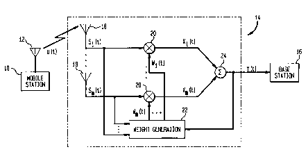
Referring to FIG. 1 there is shown a block diagram of a type of signal
processing
used in a base station applique. A signal u(t) transmitted by a mobile station
10 through
a mobile antenna 12 is received by a base station 16 at M antennas 18, with
received
~~q~~~~
signals sl(t) to s,,~(t), respectively. The received signals are weighted
using multipliers
20 having weights w~(t) to w,u(t), respectively, to generate corresponding
weighted
signals xl(t) to x,,,~(t). The weighted signals x~(t) to x,~(t) are then
combined using
summer 24 to generate an output signal y(t) which is then provided to the base
station
equipment. Weights w~(t) to w,u(t) are generated by weight generation
circuitry 22 using
the received signals s~(t) to s,u(t) and output signal y(t). At the applique
processor
circuitry 14, received signals s,(t) to s,~f(t) are weighted and combined to
improve signal
quality at the output. In one embodiment, the weights are adjusted to minimize
the
mean-squared-error in the output signal.
Referring to FIG. 2 there is shown an existing base station with an adaptive
antenna applique. An existing base station 30 consists of one transmit antenna
32 and
two receive antennas 34. Signals received by the receive antennas 34 are
coupled to a
corresponding receiver multicoupler 38, which splits received signals soft)
and s~(t) to a
location receiver 40, control channel transceiver 42, N 1 traffic channel
transceivers 44,
and traffic channel transceiver 48, one transceiver per traffic channel. For
each traffic
channel, tragic channel transceiver 44 uses received signals soft) and s~(t)
from receive
antennas 34 to generate an output voice signal. The voice signals out of the
traffic
channel transceiver 44 are fed to cell site controller 46 and then passed to
mobile
telephone switching office MTSO 59.
To add processing such as that shown in FIG. l, an antenna applique can be
added to the base station, with an exemplary embodiment as shown in FIG. 2,
illustratively for improving the performance of traffic channel transceiver
48. The added
circuitry 56 has two additional receive antennas 58. Signals received by the
additional
receive antennas 58 are coupled to corresponding receiver multicouplers 50 as
in current
base station 30. Signals from the receive antennas soft) to sj(t) are then
processed by
adaptive antenna applique 52, which generates output signal y(t) that is fed
to traffic
channel transceiver 48. In FIG. 2, switches 54 permit an input signal of the
traffic
channel transceiver 48 to be switched between the existing base station 30 and
the
adaptive antenna applique 52. In this embodiment the addition of the adaptive
applique
52 requires no modification of the existing base station 30.
~~95489
6
Refernng to FIG. 3 there is shown further detail of the adaptive antenna
applique
52 of FIG. 2. Received signals soft) to sj(t) from multicouplers 38 and 50 in
FIG. 2 are
converted from RF to baseband, or to IF, by RF downconverters 60. Output
signals volt)
to vj(t) from downconverters 60 are then converted to digital samples by A/D
converters
62, and the digital samples are processed by digital signal processing
circuitry 64. The
digital signal processing circuitry 64 generates an output signal a(t) which
is converted
to an analog signal by D/A converter 66 and upconverted to the received
carrier
frequency by Transmit Modulator/Upconverter circuitry 68, and the output
signal is
then coupled to base station traffic channel transceiver 48 in FIG. 2. The
applique
processes received signals soft) to sj(t) so as to generate an output signal
which appears
to the base station 30 in FIG. 2 to have come from a standard antenna, i.e.,
the applique
processing is transparent to the base station 30.
A key issue for transparency is the delay introduced. The adaptive antenna
applique 52 shown in FIG. 3 can require a significant amount of processing
time in
comparison to the propagation delay typically encountered in mobile radio
systems. A
large portion of that delay is in the calculation of adaptive weights for
optimum
combining.
The delay may be better understood by considering illustratively the North
American Digital Mobile Radio Standard IS-136. Referring to FIG. 4A there is
shown
the TDMA frame 70 and time slots 72. Referring to FIG. 4B there is shown in
detail a
time slot structure 72 of IS-136 uplink (mobile station to base station)
digital traffic
channel. This is a time-division multiple access (TDMA) frame structure,
wherein data
transmitted from each mobile station (cellular phone) user is transmitted
periodically in
time slots 72 or "bursts". There are 6 time slots 72 defined per frame 70. The
duration of
frame 70 is 40 ms, and each of time slots 72 is one-sixth of the frame
duration,
approximately 6.7 ms.
When full rate voice coders are used, three users are assigned per channel,
with
each user transmitting in two of the six time slots, i.e., in time frame 70
the first and
fourth time slots 72 for the first user, the second and fifth time slots 72
for the second
user, and the third and sixth time slots 72 for the third user. Each time slot
72 comprises
162 symbols, including synchronization (SYNC) sequence 74. The SYNC 74
7 ~1954~9
comprising symbols 15 through 28. This synchronization sequence is fixed and
known
a priori at the receiver. In order to compute the applique's adaptive weights
for the
purpose of interference cancellation, e.g. as described in "Signal Acquisition
and
Tracking with Adaptive Arrays in the Digital Mobile Radio System IS-54 with
Flat
Fading," by Jack Winters, IEEE Trans. on Vehicular Technology, November 1993,
it is
advantageous to have prior knowledge of some symbols within each time slot,
and
SYNC 74 sequence, although not intended originally for this purpose,
nevertheless
provides this capability. Thus, before the applique can compute the adaptive
weights, it
must acquire at least the first 28 symbols of the burst. This results a delay
of at least 28
symbols (approximately 1152 sec) for acquisition alone, even if no subsequent
processing delays were incurred in the applique; and in fact the subsequent
processing
delays for actually computing the adaptive weights and deriving the applique
output
signal would typically exceed this delay significantly. Although IS-136 base
station
receivers are designed to accommodate delays due to signal propagation, such
delays
1 S are on the order of a few symbols. Thus the delays required for applique
adaptive
weight processing inherently exceed the ability of existing IS-136 receivers
to operate
within the delay allocated for propagation effects.
Referring to FIG. 5 there is shown a block diagram of the equipment used to
test
the effect of delay on an IS-54 base station. It should be noted that IS-54
utilizes a
traffic channel format identical to IS-136. An IS-54 cellular phone 80
communicates
with IS-54 base station emulator 82 through circuitry 84 which introduces
delay in the
mobile-to-base path. Duplexers 86 and 87 separate the transmit and receive
signals,
with the signal transmitted from the base connected directly to cellular phone
80
through the duplexers 86 and 87. The signal transmitted from cellular phone 80
goes
through duplexer 86 into RX downconverter/demodulator 88 where it is converted
to
baseband signals b,(t) and bQ(t), the inphase and quadrature components
respectively,
using carrier signal c(t) from local oscillator 90. Baseband signals bi(t) and
bQ(t) are
then converted to digital signals e,(t) and eQ(t) using A/D converters 92, and
digital
signals e,(t) and eQ(t) are processed by a digital signal processor contained
in a delay
circuitry 94 to introduce an adjustable delay. Delayed digital output signals
fl(t) and fQ(t)
are then converted back to analog baseband signals g,(t) and gQ (t) by D/A
converters
CA 02195489 2000-07-19
8
96, and upconverted to the carrier frequency by TX modulator/upconverter 98,
using
carrier signal c(t) from local oscillator 90. Delayed analog signal h(t) is
then fed the
base station emulator 82 through duplexer 87.
When a cellular phone call is initially set up with no delay in the uplink
path,
it was observed that if additional delay of more than a few symbols, but much
less
than 20 ms, was introduced, then the call is dropped. However, if the
introduced
delay was very close to 20 ms, i.e., if the signal is delayed so as to align
with the next
time slot for that user, then the call is not dropped. It was observed that
calls would
remain up with delays of multiples of 20 ms, up to 200 ms. With delays in this
range,
base station emulator 82 was still able to perform the administrative
functions of
mobile transmit power adjustment and mobile time alignment. However, it was
not
able to successfully complete inter-slot handoffs unless the delay was 3 or
fewer
times the 20 ms intra-user burst delay. Thus an applique approach is feasible
if the
delay is a small integer multiple of the intra-user burst delay.
Again referring to FIG. 3 there is shown a plurality of received signals
So f t) . . . S3(t) which are converted and digitized for processing by the
digital signal
processor (DSP) 64. Referring to FIG. 6 in conjunction with FIG. 3, it can be
seen
that the processing comprises selecting a predetermined symbol pattern, within
a
sync sequence 74 (shown in FIG. 4B), within a time slot 72 (shown in FIG. 4B)
in
step 102. Generating weights, wherein a mean squared error of the output
signal is
minimized in step 104. Weighing and combining the received signals in step 106
using the generated weights from step 104 to provide a processed signal.
Delaying
the processed signal in step 108 to correspond with a later data burst.
Numerous modifications and alternative embodiments of the invention will be
apparent to those skilled in the art in view of the foregoing description.
Accordingly,
this description is to be construed as illustrative only and is for the
purpose of
teaching those skilled in the art the best mode of carrying out the invention.
Details
of the structure may be varied substantially without departing from the spirit
of the
invention and the exclusive use of all modifications which come within the
scope of
the appended claim is reserved.