Note: Descriptions are shown in the official language in which they were submitted.
21 q5~0~
SPECIFICATION
Tille of the Invention
SUPE~CONDUCTING DEVICE HAVING AN
S EXTREMELY THIN SUPERCONDUCTING CHANNEL
FORMED OF OXIDE SUPERCONDUCTOR MATERIAL
AND METHOD FOR MANUFACTURING THE SAME
Background of the Invention
Field of the invention
The present invention relates to a superconducting device and a
me thod for manufacturing the same, and more specifically to a
superconducting device having an extremely thin superconducting ch~nnel
formed of oxide superconductor material, and a method for
manufacturing the same.
Description of related art
Devices which utilize superconducting phenomena operate rapidly
with low power consumption so that they have higher performance than
conventional semiconductor devices. Particularly, by using an oxide
superconducting material which has been recently advanced in study, it is
pos,sible to produce a superconducting device which operates at relatively
high temperature.
Josephson device is one of well-known superconducting devices.
However, since Josephson device is a two-terminal device, a logic gate
which utilizes Josephson devices becomes complicated configuration.
Therefore, three-terminal superconducting devices are more practical.
21 9580q
Typical three-terminal superconducting devices include two types of
super-FET (field effect transistor). The first type of the super-FET
includes a semiconductor channel, and a superconductor source electrode
and a superconductor drain electrode which are formed closely to each
S other on both side of the semiconductor channel. A portion of these]~iconductor layer between the superconductor source electrode and dle
superconductor drain electrode has a greatly recessed or undercut rear
surface so as to have a reduced thickness. In addition, a gate electrode is
fo]med through a gate insulating layer on the portion of the recessed or
undercut rear surface of the semiconductor layer between the
superconductor source electrode and the superconductor drain electrode.
A superconducting current flows through the semiconductor layer
(channel) between the superconductor source electrode and the
superconductor drain electrode due to the superconducting proximity
effect, and is controlled by an applied gate voltage. This type of the
super-FET operates at a higher speed with a low power consumption.
The second type of the super-FET includes a channel of a
superconductor formed between a source electrode and a drain electrode,
so that a current flowing through the superconducting channel is
2 0 controlled by a voltage applied to a gate formed above the
superconducting channel.
Both of the super-FETs mentioned above are voltage controlled
devices which are capable of isolating output signal from input one and of
having a well defined gain.
2 5 However, since the first type of the super-FET utilizes the
superconducting proximity effect, the superconductor source electrode
and the superconductor drain electrode have to be positioned within a
21 9~9
distance of a few times the coherence length of the superconductor
materials of the superconductor source electrode and the superconductor
drain electrode. In particular, since an oxide superconductor has a short
coherence leng~, a distance between the superconductor source electrode
S and ~e superconductor drain electrode has to be made less than about a
fe~w ten nanometers, if the superconductor source electrode and the
sujperconductor drain electrode are formed of the oxide superconductor
material. However, it is very difficult to conduct a fine processing such
as a fine pattern etching, so as to satisfy the very short separation distance
10 mentioned above.
On the other hand, the super-FET having the superconducting
channel has a large current capability, and the fine processing which is
required to product the first type of the super-FET is not needed to
product this type of super-FET.
In order to obtain a complete ON/OFF operation, both of the
su]perconducting channel and the gate insulating layer should have an
extremely thin thickness. For example, the superconducting channel
formed of an oxide superconductor material should have a thickness of
les,s than five nanometers and the gate insulating layer should have a
2 0 thickness more than ten nanometers which is sufficient to prevent a tunnel
cu rrent.
In the super-FET, since the extremely thin superconducting channel
is Iconnected to the relatively thick superconducting source region and the
superconducting drain region at their lower portions, the superconducting
25 culrrent flows substantially horizontally through the superconducting
ch;mnel and subst~nti~lly vertically in the superconducting source region
an~ the superconducting drain region. Since the oxide superconductor has
- 3 -
21 ~80~ 1
the largest critical current density Jc in the direction perpendicular to
c-axes of its crystal lattices, the superconducting channel is preferably
fol~ned of a c-axis oriented oxide superconductor thin film and the
superconducting source region and the superconducting drain region are
S pre:ferably fornned of a-a~is oriented oxide superconductor thin films.
~ a prior art, in order to manufacture the super-FET which has the
superconducting channel of c-axis oriented oxide superconductor thin film
and the superconducting source region and the superconducting drain
region of a-axis oriented oxide superconductor thin films, a c-axis
oriented oxide superconductor thin film is formed at first and the c-axis
ori,ented oxide superconductor thin film is etched and removed excluding
a por~tion which will be the superconducting channel. Then, an a-axis
oriented oxide superconductor thin film is deposited so as to fornn the
superconducting source region and the superconducting drain region.
In another prior art, at first an a-axis oriented oxide
superconductor thin fil~n is deposited and etched so as to form the
superconducting source region and the superconducting drain region, and
then a c-axis oriented oxide superconductor thin film is deposited so as to
form the superconducting channel.
However, in the prior art, the oxide superconductor thin film is
degraded during the etching so that the superconducting characteristics is
affected. In addition, the etched surface of the oxide superconductor thin
filnn is roughened, therefore, if another oxide superconductor thin film is
formed so as to contact the rough surface, an undesirable Josephson
2 5 junction or a resistance is generated at the interface.
By this, the super-FET manufactured by the above conventional
process does not have an enough performance.
219580~ 1
A superconducting device as disclosed herein may comprise a
substrate having a principal surface, a non-superconducting oxide layer
ha.ving a similar crystal structure to that of the oxide superconductor, a first
and a second superconducting regions formed of c-axis oriented oxide
5 su.perconductor thin films on the non-superconducting oxide layer
separated from each other and gently inclining to each other, a third
superconducting region formed of an extremely thin c-axis oriented oxide
superconductor thin film between the first and the second superconducting
regions, which is continuous to the first and the second superconducting
10 regions.
Upper surfaces of the first and second superconducting regions gently
incline to the third superconducting region of an extremely thin oxide
superconductor thin film. Therefore, superconducting current flows into or
flows from the third superconducting region efficiently so that the current
15 capability of the superconducting device can be improved.
Preferably the third superconducting region forms a weak link of a
Josephson junction, so that the superconducting devicc
~ 2i958Q~ I
constitutes a Josephson device. In this case, the third superconducting
region preferably includes a grain boundary which constitutes a weak link
of a Josephson junction.
In another preferred embodiment, the third superconducting region
5 fo~ms a superconducting channel, so that superconducting current can
flc\w between the first and second superconducting region through ~e
third superconducting region. In this case, it is preferable that the
superconducting device further includes a gate electrode formed on the
third superconducting region, so that the superconducting device
10 constitutes a super-FET, and the superconducting current flowing between
the first and second superconducting region through the third
superconducting region is controlled by a voltage applied to the gate
electrode.
The non-superconducting oxide layer preferably has a similar
crystal structure to that of a c-axis oriented oxide superconductor thin
filIn. In this case, the superconducting channel of a c-axis oriented oxide
superconductor thin film can be easily formed.
Preferably, the above non-superconducting oxide layers is formed
2 0 of a PrlBa2Cu3O7 ~ oxide. A c-axis oriented PrlBa2Cu3O7 ~ thin film has
almost the same crystal lattice structure as that of a c-axis oriented oxide
superconductor thin film. It compensates an oxide superconductor thin
filrn for its crystalline incompleteness at the bottom surface. Therefore, a
c-axis oriented oxide superconductor thin film of high crystallinity can be
2 5 easily forrned on the c-axis oriented PrlBa2Cu3O7 ~ thin film. In addition,
the effect of diffusion of the constituent elements of Pr1Ba2Cu3O7 ~ into
the oxide superconductor thin film is negligible and it also prevents the
~ ~19~G9
diffusion from substrate. Thus, the oxide superconductor thin film
deposited on the PrlBa2Cu307 ~ thin film has a high quality.
In a preferred embodiment, the oxide superconductor is formed of
high-TC (high critical temperature) oxide superconductor, particularly,
S folmed of a high-TC copper-oxide type compound oxide superconductor
for example a Y-Ba-Cu-O compound oxide superconductor material, a
Bi-Sr-Ca-Cu-O compound oxide superconductor material, and a
Tl-Ba-Ca-Cu-O compound oxide superconductor material.
In addition, the substrate can be formed of an insulating substrate,
10 preferably an oxide single crystalline substrate such as MgO, SrTiO3,
CdNdA104, etc. These substrate materials are very effective in forming
or growing a crystalline film having a high degree of crystalline
orientation. However, the superconducting device can be formed on a
senniconductor substrate if an appropriate buffer layer is deposited
15 thereon. For example, the buffer layer on the semiconductor substrate
can be formed of a double-layer coating formed of a MgA104 layer and a
BaTiO3 layer if silicon is used as a substrate.
Another form of superconducting device may comprise a substrate, a
2 ~ non-superconducting layer formed on a principal surface of said
substrate, an extremely thin superconducting channel formed of an oxide
sup~erconductor thin film on the non-superconducting layer, a
superconducting source region and a superconducting drain region of a
relatively thick thickness formed of the oxide superconductor at the both
25 sides of the superconducting channel separated from each other but
electrically connected through the superconducting channel, so that a
superconducting current can flow through the superconducting channel
~ ~195~9
between the superconducting source region and the superconducting drain
region, and a gate electrode through a gate insulator on the
sulperconducting channel for controlling the superconducting current
flowing through the superconducting channel, in which the
S su~perconducting channel is connected to the superconducting source
region and the superconducting drain region at the height of their middle
portions.
According to still another embodiment disclosed herein
a superconducting device comprises a substrate having a
10 principal surface, a non-superconducting oxide layer having a similar
cr~stal structure to that of the oxide superconductor, two superconducting
re~rions formed of a c-axis oriented oxide superconductor thin film
separated by an insulating region positioned between them, an extremely
thin superconducting region formed of a c-axis oriented oxide
15 superconductor thin film on the insulating region, which is continuous to
the two superconducting regions and forms a weak link of Josephson
junction, in which the two superconducting regions and the insulating
re~ion are formed of one c-axis oriented oxide superconductor thin film
which has a gently concave upper surface and of which the center portion
2 0 includes much impurity so that the portion does not show
superconductivity.
According to a fourth aspect disclosed herein, there is
prc,vided a superconducting device comprising a substrate having a
principal surface, a non-superconducting oxide layer having a similar
25 crystal structure to that of the oxide superconductor, a superconducting
source region and a superconducting drain region formed of a c-axis
oriented oxide superconductor thin film separated from each other, an
21 q5~G9
e~tremely thin superconducting channel formed of a c-axis oriented oxide
superconductor thin filnn on the non-superconducting oxide layer, which
e].ectrically connects the superconducting source region to the
s~lperconducting drain region, so that superconducting current can flow
S ~lrough the superconducting channel between ~e superconducting source
region and the superconducting drain region, and a gate electrode through
a gate insulator on the superconducting channel for controlling the
sllperconducting current flowing ~rough the superconducting channel, in
which the superconducting source region and the superconducting drain
10 region have upper surfaces gently inclined to the superconducting
ch~nnel.
According to a fifth aspect of the superconducting device, the
device comprises a substrate having a principal surface, a non-
15 superconducting oxide layer having a similar crystal structure to that of theoxide superconductor, two superconducting regions formed of c-axis
or:iented oxide superconductor thin films separated from each other, an
extremely thin superconducting regions formed of a c-axis oriented oxide
superconductor thin film on the non-superconducting oxide layer, which
2 o continuous to the two superconducting regions and forms a weak link of a
Josephson junction, in which the two superconducting regions have upper
su:rfaces gently inclined to the weak link.
Summary of the Invention
According to the present invention, there is provided a
25 superconducting device comprising a substrate, a non-superconducting
layer formed on a principal surface of said substrate, an extremely thin
superconducting channel formed of an oxide superconductor thin film on
the non-superconducting layer, a-
g
~ ~195~9
superconducting source region and a superconducting drain region of arelatively thick thickness formed of the oxide superconductor at the both
sid,es of the superconducting channel separated from each other but
electrically connected through the superconducting channel, so that a
S superconducting current can flow through the superconducting channel
bel;ween the superconducting source region and the supercon~ ctin~ drain
re~gion, and a gate electrode through a gate insulator on the
superconducting channel for controlling the superconducting current
flowing through the superconducting channel, in which the
10 superconducting channel is connected to the superconducting source
region and the superconducting drain region at the height of their middle
portions.
A method for manufacturing a superconducting device
15 may comprise the steps of forming on a principal surface of a substrate a
non-superconducting oxide layer having a similar crystal structure to that
of the oxide superconductor, forming a first oxide superconductor thin
filrn having a relatively thick thickness on the non-superconducting oxide
layer, etching the first oxide superconductor thin film so as to form a
2 0 concave portion which is concave gently on its center portion, implanting
ions to the first oxide superconductor thin film at the bottom of the
concave portion so as to form an insulating region and the first oxide
superconductor thin film is divided into two superconducting regions by
the insulating region, and forming a second extremely thin oxide
2 5 superconductor thin film on the insulating region and the two
superconducting regions which is continuous to the two superconducting
re,~,ions.
10- 1
21 958~9
In one preferred embodiment, the ions which are implanted so as to
folm the insulating region are selected from Ga ions, Al ions, In ions, Si
ions, Ba ions and Cs ions.
It is preferable that the second extremely thin oxide superconductor
S thin film is formed to have a grain boundary in it so as to form a weak
link of Josephson junction. It is also preferable that the second extremely
thin oxide superconduc~or thin film is formed so as to constitute a
superconducting channel through which superconducting current flows
between the two superconducting regions. In this case, the method
10 further includes the steps of forming a gate insulating layer on the second
extremely thin oxide superconductor thin film at a portion above the
ins,ulating region and forming a gate electrode on the gate insulating
layer.
According to another aspect of the method disclosed herein
15 foI manufacturing a superconducting device, the me~od comprises
the steps of forming on a principal surface of a substrate a
no]n-superconducting oxide layer having a similar crystal structure to that
of the oxide superconductor, forming a first oxide superconductor thin
film having a relatively thick thickness on the non-superconducting oxide
2 0 layer, etching the first oxide superconductor thin film so as to divide intotwo superconducting regions by the insulating region which have inclined
surfaces gently inclined to each other and the non-superconducting oxide
layer is exposed between them, and forming a second extremely thin
ox ide superconductor thin film on the exposed portion of the
25 non-superconducting oxide layer and the two superconducting regions
which is continuous to the two superconducting regions.
~ 2~958~9
In one preferred embodiment, the second extremely thin oxide
superconductor thin film is formed to includes a grain boundary in it so
as to constitute a weak link of Josephson junction. It is also preferable
that the second extremel~ thin oxide superconductor thin film is formed
S so as to constitute a superconducting channel of a super-FET. In this case,
the method preferably further includes the steps of forming a gate
ins~ tin~ layer on the second extremely thin oxide superconductor thin
film at a portion above the the exposed portion of the
non-superconducting oxide layer and forming a gate electrode on the gate
1 0 insulating layer.
According to another aspect of the present invention, there is
provided a method for manufacturing a superconducting device,
cornprising the steps of ~orming on a principal surface of a substrate a
firsit oxide superconductor thin film having a relatively thick thickness,
15 forming a metal layer on the first superconductor thin film, forming a
SiC)2 layer on the metal layer, selectively etching a center portions of the
SiC)2 layer, the metal layer and the first oxide superconductor thin film so
that the portions of the SiO2 layer, the metal layer and the first oxide
suplerconductor thin film is completely removed and a surface of the
2 0 sub~strate is exposed so as to form a superconducting source region and a
superconducting drain region separately on the substrate and a source
electrode and a drain elec~rode respectively on the superconducting source
region and the superconducting drain region, forming a
non-superconductor layer having a half thickness of the superconducting
25 source region and the superconducting drain region on the exposed
surface of the substrate, forming a second extremely thin oxide
superconductor thin film on the non-superconducting layer so that an
- 12-
~ ~195~
extremely thin superconducting channel which is connected to the
sujperconducting source region and the superconducting drain region at
~e height of the middle portions is formed on the non-superconducting
er, forming a gate ins~ tin~ layer and a gate electrode stacked on the
5 gate ins~ tin~ layer on a portion of the second oxide superconductor thin
fillm above the non-superconducting layer, and removing the sio2 layer so
that the source electrode ~nd the drain electrode are exposed.
It is preferable tha~ the SiO2 layer is removed by using a weak HF
solution.
According to another aspect of the method disclosed herein
fo] manufacturing a superconducting device, the me~hod comprises
~u~ steps of forming on a principal surface of a subs~rate a
lifl:-off layer, removing the lift-off layer excluding a portion at which a
projecting insulating region will be formed, etching the principal surface
l 5 of a substrate so that a projecting insulating region of which the cross
section is a shape of a trapezoid is formed on the principal surface,
folming a first oxide superconductor thin film on the principal surface
and the projecting insulating region, removing the remaining lift-off layer
so that the first oxide superconductor thin film is divided into a
superconducting source region and a superconducting drain region and a
surface of the projecting insulating region is exposed, forming a second
oxiide superconductor thin film on the projecting insulating region which
constitutes a superconducting channel, and forming a gate insulating layer
and gate electrode on the superconducting channel.
2 5 In one preferred embodiment, the lift-off layer is preferably
formed of a CaO layer of which surface is covered with a Zr layer. This
lift-off layer can be removed by ~1ti1i7ing water and following reaction:
- 13 -
~ 21 ~8~ 1
CaO + H20 ~ Ca(OH)2
In the above process, no reactive agent is used but water.
Therefore, if the flat-top projection is formed by the above process, the
substrate and the supercomducting thin film are not degraded.
S The above and other objects, features and advantages of ~e present
in~ention will be apparent from the following description of preferred
e~lbodiments of the invention with reference to the accompanying
drawings.
Brief Description of the Drawings
Figures lA to lF are diagrammatic sectional views for illustrating a
first embodiment of a process for manufacturing the super-FET;
Figures 2A to 2C are diagrammatic sectional views for illustrating
featured steps of a second embodiment of the process for manufacturing the
1 5 super-FET;
Figures 3A to 3J are diagrammatic sectional views for illustrating a
third embodiment of the process for manufacturing the super-FET; and
Figures 4A to 4J are diagrammatic sectional views for illustrating a
fourth embodiment of the process for manufacturing the super-FET.
Description of the Preferred embodiments
Em~bodiment 1
Referring to Figures lA to lF, a process for manufacturing the super-
FET will be described.
- 14-
~ 2~809
As shown in Figure lA, a MgO (100) single crystalline substrate 5
ha~ving a subst~nti~lly planar principal surface is prepared.
As shown in Figure lB, an oxide layer 20 having a thickness of 100
nanometers composed of a c-axis oriented PrlBa2Cu307.~ thin film is
S deposited on the principal surface of the substrate S and a c-axis oriented
YlBa2Cu307 ~ oxide superconductor thin film 1 having a thickness of
about 300 nanometers is deposited on the oxide layer 20, by for example a
sputtering, an MBE (molecular beam epitaxy), a vacuum evaporation, a
CVD, etc. A condition of forming the c-axis oriented PrlBa2Cu3O7 ~ thin
film and the c-axis oriented YlBa2Cu3O7 ~ oxide superconductor thin film
1 by off-axis sputtering is as follows:
Prl Ba2Cu3O7 ~ thin film
Temperature of the substrate 750 ~C
Sputtering Gas Ar: 90%
1 5 ~2: 10%
Pressure 10 Pa
YlBa2Cu3O7 ~ oxide superconductor thin film
Temperature of the substrate 700 ~C
Sputtering Gas Ar: 90%
~2 10%
Pressure 10 Pa
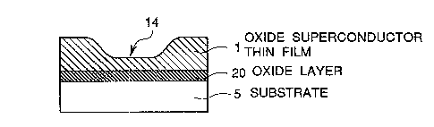
Then, as shown in lFigure lC, a center portion of the YlBa2Cu307 ~
oxide superconductor thin film 1 is processed by He ion-beam accelerated
by an energy of 3 to 50 keV so as to form a concave portion 14 which is
2 5 concave gently. The tilt angle of the concave portion 14 is less than 40~ and its length is about 100 nanometers.
~ 21958U9
Thereafter, Ga ions are implanted into a bottom portion of the
concave portion 14 by an energy of S0 to lS0 keV so as to form an
insulating region S0, as shown in Figure lD. In this connection, Al ions,
In ions, Si ions, Ba ions ~nd Cs ions can be also used instead of Ga ions.
S The YlBa2Cu307 ~ oxidle superconductor thin film 1 is divided into a
superconducting source region 2 and a superconducting drain region 3 by
~e ins~ ting region S0.
Then, the substrate S is heated to a temperature of 350 to 400 ~C
un~der a pressure lower than 1 x 10⁻⁹ Torr so as to clean the surface of the
10 Y1Ba2Cu3O7 ~ oxide superconductor thin film 1. This heat-treatment is
not necessary, if the surf~ce of the YlBa2Cu307 ~ oxide superconductor
thin film 1 is clean enough.
Thereafter, as shown in Figure lE, a c-axis oriented YlBa2Cu3O7~
oxide superconductor thin film 11 having a thickness on the order of
15 about 5 nanometers is deposited on the surface of the YlBa2Cu3O7,~ oxide
superconductor thin film 1 by an MBE (molecular beam epitaxy). A
co]ndition of forming the c-axis oriented YlBa2Cu307~ oxide
superconductor thin film 11 by an MBE is as follows:
Molecular beam source Y: 1250~C
2 0 Ba: 600~C
Cu: 1040~C
~2 or 03 atmosphere
Pressure 1 x 10⁻⁵ Torr
Temperature of the substrate 700~C
. 25 Since the YIBa2Cu307~ oxide superconductor thin film 11 is
formed on the gently curved surface of the YlBa2Cu307~ oxide
superconductor thin film 1, it becomes an uniform c-axis oriented oxide
- 16-
~1 9~809
superconductor thin film. A portion of the YlBa2Cu3O7~ oxide
superconductor thin film 11 on the insulating region 50 becomes a
superconducting channel.
Finally, as shown in Figure lF, a gate ins~ tin~ layer 7 is formed
5 of Si3N4, MgO or SrTiO3 on the superconducting channel 10 and a gate
electrode 4 is formed of Au on thLe gate insulating layer 7. Metal
electrodes may be formedl on the superconducting source region 2 and the
superconducting drain region 3, if necessar~r. With this, the super-FET in
accordance with the present invention is completed.
As explained above, the superconducting channel, the
superconducting source region and the superconducting drain region of
the above mentioned super-FET manufactured in accordance with the
embodiment of the method of the present invention are formLed of c-axis
oriented oxide superconductor thin films. Therefore, the super-FET has
15 no undesirable resistance nor undesirable Josephson junction between the
superconducting channel and the superconducting source region and
between the superconducting channel and the superconducting drain
region. In addition, since the superconducting source region and the
superconducting drain region gently inclines to the superconducting
20 chaLnnel, superconducting current efficiently flows into and flows from
the superconducting channel. By this, the current capability of the
super-FET can be improved.
In the above method, if the YlBa2Cu307 ~ oxide superconductor thin
film 11 is deposited to have a grain boundary so as to formL a weak link of
25 the Josephson junction on the insulating region 50, a Josephson junction
device is manufactured. In this case, the superconducting source region
andl the superconducting drain region are two superconducting electrodes.
. ~ 21~5809
Al]most all the above mentioned features of the super-FET can apply to
~e Josephson junction de~rice.
Embo~liment 2
Referring to Figures 2A to 2C, a second embodiment of the process
for manufacturing ~e superconducting device will be described.
In this second embodiment, the same processings as those shown in
Fi~ures lA to lB are performed.
Then, as shown in Figure 2A, the YIBa2Cu3O7 ~ oxide
superconductor thin film 1 is processed by He ion-beam accelerated by an
energy of 3 to 50 keV so l;hat the YlBa2Cu3O7 ~ oxide superconductor thin
film 1 is divided into a superconducting source region 2 and a
superconducting drain region 3 which have inclined surfaces gently
inclined to each other. The tilt angle of the inclined surfaces is less than
40". The oxide layer 20 of PrlBa2Cu3O7 E is exposed between the
superconducting source region 2 and the superconducting drain region 3.
Then, the substrate S is heated to a temperature of 350 to 400 ~C
under a pressure lower than 1 x 10⁻⁹ Torr so as to clean the surfaces of
the superconducting source region 2 and the superconducting drain region
3 and the exposed surface of the oxide layer 20. This heat-treatment is
not necessary, if the surfaces of the superconducting source region 2 and
the superconducting drain region 3 and the exposed surface of the oxide
layer 20 are clean enough.
Thereafter, as shown in Figure 2B, a c-axis oriented YIBa2Cu3O7 ~
oxide superconductor thin film 11 having a thickness on the order of
about S nanometers is deposited on the surfaces of the superconducting
source region 2 and the superconducting drain region 3 and the exposed
- 18 -
2i 95809
sul~face of the oxide layer 20 by an MBE (molecular beam epitaxy). A
condition of forming the c-axis oriented Y1Ba2Cu3O 7 ~ oxide
su]?erconductor thin film 11 by an MBE is the same as that of
Embodiment 1.
S Since the YIBa2Cu307~ oxide superconductor thin filrn 11 is
fol~ned on the gently curved surfaces of the superconducting source
re~sion 2 and the superconducting drain region 3 and the exposed surface
of the oxide layer 20, it becomes an uniform c-axis oriented oxide
superconductor thin film. A portion of the YlBa2Cu3O7 ~ oxide
1 0 superconductor thin film 11 on the exposed surface of the oxide layer 20
becomes a superconducting channel 10.
Finally, as shown in Figure 2C, a gate insulating layer 7 is formed
of Si3N4, MgO or SrTiO3 on the superconducting channel 10 and a gate
electrode 4 is formed of Au on the gate insulating layer 7. Metal
electrodes may be formed, on the superconducting source region 2 and the
superconducting drain region 3, if necessary. With this, the super-FET in
accordance with the present invention is completed.
As explained above, the superconducting channel, the
superconducting source region and the superconducting drain region of
the above mentioned super-FET manufactured in accordance with the
embodiment of the method of the present invention are formed of c-axis
ori~nted oxide superconductor thin films. Therefore, the super-FET has
no undesirable resistance nor undesirable Josephson junction between the
superconducting channel and the superconducting source region and
between the superconducting channel and the superconducting drain
region. In addition, since the superconducting source region and the
superconducting drain region gently inclines to the superconducting
2 ~ ~ 5 ~
channel, superconducting current efficiently flows into and flows from
the superconducting channel. By this, the current capability of the
super-FET can be improved.
In ~e above method, if the YlBa2Cu307 ~ oxide superconductor thin
S fi~n 11 is deposited to have a grain boundary so as to form a weak link of
~ Josephson junction on the exposed surface of the oxide layer 20, a
Jo sephson junction device is manufactured. In this case, the
superconducting source region and the superconducting drain region are
tw3 superconducting electrodes. Almost all the above mentioned features
10 of the super-FET can apply to the Josephson junction device.
Embodiment 3
Referring to Figures 3A to 3J, a third embodiment of the process
for m~nl~facturing the superconducting device will be described.
As shown Figure 3A, an MgO (100) substrate 5 similar to that of
Embodiment 1 is prepared. As shown in Figure 3B, a c-axis oriented
YlBa2Cu3O7 ~ oxide superconductor thin film 1 having a thickness of
about 250 nanometers is deposited on a principal surface of a MgO
substrate 5, by for example a sputtering, an MBE (molecular beam
20 epitaxy~, a vacuum evaporation, a CVD, etc. A condition of forming the
c-axis oriented YlBa2Cu3O7 ~ oxide superconductor thin film 1 by off-axis
sputtering is as follows:
Temperature of the substrate 700~C
Sputtering Gas Ar: 90%
~2 10%
Pressure 5 x 10⁻² Torr
- 20 -
'~ ~IqS809
Then, as shown in Figure 3C, an Au layer 14 having a thickness of
30 to 100 nanometers is formed on the YIBa2Cu3O7 ~ oxide
superconductor thin film 1. As shown in Figure 3D, a sio2 layer 15
ha~ving a thickness of 250 nanometers is formed on the Au layer 14 by a
5 C~D. A center portion of the sio2 layer 15 is removed by using a
photoli~ography. Using the processed sio2 layer 15 as a mask, center
portions of the Au layer 14 and the YlBa2Cu307 ~ oxide superconductor
thin film 1 are selectively etched by a reactive ion etching using a chloric
gas" an ion milling using Ar-ions or a focused ion beam etching so that the
10 Au layer 14 is divided into a source electrode 12 and a drain electrode 13,
the YlBa2Cu3O7 ~ oxide superconductor thin film 1 is divided into a
superconducting source region 2 and a superconducting drain region 3,
an~1 a portion 16 of the surface of the substrate 5 is exposed between
them, as shown in Figure 3E.
Then, the substrate S is heated to a temperature of 350 to 400 ~C
under a pressure lower than 1 x 10⁻⁹ Torr so as to clean the exposed
surface 16 of the substrate 5. This heat-treatment is not necessary, if the
exposed surface 16 of the substrate 5 is clean enough. As shown in Figure
3F, an oxide layer 20 composed of c-axis oriented PrlBa2Cu3O7 ~ is
20 deposited on the exposed surface 16 of the substrate 5, by an MBE. The
oxide layer 20 preferably has a half thickness of the superconducting
source region 2 and the superconducting drain region 3. While the
Pr]Ba2Cu307 ,~ thin film 20 is growing, the surface morphology of the
PrlBa2Cu3O7 ~ thin film 20 is monitored by RHEED. A condition of
2 5 forming the c-axis oriented PrlBa2Cu3O7 ~ oxide thin film 20 by MBE is
as irollows:
Molecular beam source Pr: 1225~C
- 21 -
~ 2195809
Ba: 600~C
Cu: 1040~C
Pressure 1 x 10⁻⁵ Torr
Temperature of the substrate 750~C
S Then, the Pr molecular beam source is exchanged to a Y molecular
be~am source and the temperature of the substrate is lowered to 700 ~C so
tha~t a superconducting channel 10 of a c-axis oriented YlBa2Cu307~ oxide
superconductor thin film having a thickness of about S nanometer is
co]:ltinuously formed on the oxide layer 20 of PrlBa2Cu307 ~ thin film, as
shown in Figure 3G.
Thereafter, as shown in Figure 3H, a gate insulating layer 7 of MgO
is formed by a sputtering successively on the superconducting source
regrion 2, the superconducting channel 10 and the superconducting drain
re~rion 3. The gate insulating layer 7 has a thickness of 10 to 20
nanometers and covers side surfaces of the superconducting source region
2 a~nd the superconducting drain region 3 for their insulation.
Then, as shown in Figure 3I, a gate electrode 4 of Au is formed on
a center portion of the ga~e insulating layer 7 by a vacuum evaporation.
Finally, as shown in Figure 3J, the SiO2 layer 15 is removed by
2 0 using a 10% HF solution. Metal layers are formed on the source
electrode 12 and the drain electrode 13 respectively, so as to planarize the
upper surface of the device, if necessary. With this, the super-FET in
accordance with the present invention is completed.
The above mentioned super-FET manufactured in accordance with
2 5 the third embodiment of the method has a superconducting channel whichis formed on the PrlBa2Cu307 ~ non-superconducting oxide layer of which
the crystal structure is similar
~ I
''- 2195~09
to that of the YlBa2Cu3O7 ~ oxide superconductor. Therefore, the bottom
pa~rtion of the superconducting channel is not degraded so that the
subst~nti~l cross-sectional area of the superconducting channel of the
super-FET is larger than that of a conventional super-FET.
S Additionally, since the superconducting channel is connected to the
superconducting source region and the superconducting drain region at
~e height of their middlle portions, superconducting current ef~lciently
f~c~ws into and flows frorn the superconducting channel. By all of these,
the current capability of the super-FET can be improved.
In addition, since the substantially planarized upper surface is
obtained, it become easy to form conductor wirings in a later process.
Furthermore, according to the method the
oxide layer, the superconducting channel, the gate ins~ ting layer and the
gate electrode are self-aligned. In the above method, since the oxide
sujperconductor thin films are covered during the etching process, the
su]perconducting characteristics of the oxide superconductor thin films are
not affected. Therefore, the limitation in the fine processing technique
required for manufacturing the super-FET is relaxed, and the
m~mufactured super-FET has a excellent performance.
En~bodiment 4
Referring to Figures 4A to 4J, a forth embodiment of the process
for manufacturing the superconducting device will be described.
As shown Figure 4A, an MgO (100) substrate S similar to that of
~mbodiment 1 is prepared. As shown in Figure 4B, a lift-off layer 16 of
a CaO layer having a thickness of 1 ,um covered with Zr layer having a
thickness of 50 nanometers is deposited on the substrate 5.
21 9~D~ I
Then as shown in Figure 4C, the lift-off layer 16 is removed
excluding a portion at which a insulating region will be positioned. The
lift-off layer 16 can be processed by a dry etching using a photoresist or a
lift-off.
S Thereafter, the principal surface of ~e substrate S is etched by a
reactive ion etching, ion millin~ using Ar ions etc. In this etching
prc~cess, the rem~ining lift-off layer 16 is used as a mask so that a
prcljecting insulating region 50 of which the cross section is a shape of a
trapezoid is formed on the substrate.
Then, the substrate S is heated to a temperature of 350 to 400 ~C
under a pressure lower than 1 x 10⁻⁹ Torr so as to clean the etched
surface of the substrate 5.
Thereafter, as shown in Figure 4E, a YlBa2Cu3O7 ~ oxide
superconductor thin filrn 1 having a thickness on the order of 200 to 300
nanometers is deposited on the etched surface of the substrate 5 and the
lift-off layer 16. The YIBa2Cu307~ oxide superconductor thin film 1 is
preferably formed by an MBE (molecular beam epitaxy). A condition of
forming the YlBa2Cu3O7 ~ oxide superconductor thin film 1 by an MBE is
as i~ollows:
Molecular beam source Y: 1250 ~C
Ba: 600~C
Cu: 1040~C
~2 or 03 atmosphere
Pressure 1 x 10⁻⁵ Torr
Temperature of the substrate 680~C
Then, the lift-off layer 16 is removed so that the YlBa2Cu307 ~
oxide superconductor thin film 1 is divided into a superconducting source
- 24 -
' ~ 2iq~8U9
re,gion 2 and a superconducting drain region 3 and the insulating region
SCI is exposed, as shown in figure 4F. This lift-off process lltili7.es water
and a following reaction:
CaO + H2O ~ Ca(OH)2
S Since the lift-off process does not use an agent of high reactivity but
use only water, the YlBa2Cu307~ oxide superconductor dlin film 1 and
the substrate 5 are not degraded.
Thereafter, the substrate 5 is again heated to a temperature of 350
to 400 ~C under a pressure lower than 1 x 10⁻⁹ Torr so as to clean the
exposed ins~ tin~ region 50, the superconducting source region 2 and the
superconducting drain region 3.
Then, a c-axis oriented YIBa2Cu307~ oxide superconductor thin
film 11 having a thickness of 5 nanometers is deposited on the insulating
repion 50 by an MBE, as shown in Figure 4G. A condition of forming
1 5 the YlBa2Cu3O7 ~ oxide superconductor thin film 11 by an MBE is as
fo].lows:
Molecular beam source Y: 1250~C
Ba: 600~C
Cu: 1040~C
Pressure 1 x 10⁻⁵ Torr
Temperature of the substrate 700~C
A portion of the deposited YIBa2Cu307 ~ oxide superconductor thin
film 11 on the insulating region 50 becomes a superconducting channel
10.
2~ Then, a insulating layer 17 is formed of Si3N4, MgO or SrTiO3 on
the YlBa2Cu307,~ oxide superconductor thin film 11, as shown in
- 25 - .
58Q~ I
Fipure 4H, and an Au layer 14 on the insulating layer 17, as shown in
Figure 4I.
Finally, the Au layer 14 is processed into a gate electrode 4, the
in~ tin~s layer 17 is processed into a gate insulating layer 7, and the
sol!lrce electrode 12 and the drain electrode 13 are formed of Au on the
su]perconducting source region 2 and superconducting drain region 3.
With this, he super-FET in accordance with the present invention is
co]~pleted.
The above mentioned super-FET manufactured in accordance with
the fourth embodiment of the method has the substantially planarized
upper surface, it become easy to form conductor wirings in a later process.
Furthermore, according to the method the
superconducting channel is formed without using etching. Thus, the
superconducting channel is not affected. Therefore, the limitation in the
fine processing technique required for manufacturing the super-FET is
relaxed, and the manufactured super-FET has a excellent performance.
In the above mentioned embodiment, the oxide superconductor thin
fil]~ can be formed of not only the Y-Ba-Cu-O compound oxide
superconductor material, but also a high-TC (high critical temperature)
oxide superconductor material, particularly a high-TC copper-oxide type
compound oxide superconductor material, for example a Bi-Sr-Ca-Cu-O
co]~pound oxide superconductor material, and a Tl-Ba-Ca-Cu-O
compound oxide superconductor material.
2 5 The invention has thus been shown and described with reference to
the specific embodiments. However, it should be noted that the present
in~ention is in no way limited to the details of the illustrated structures
- 26 -
~ ~. 2 ~ 958~q
but converts and modifications may be made within the scope of the
appended claims.
- ~7 -