Language selection

Search

Patent 2196239 Summary

Third-party information liability

Some of the information on this Web page has been provided by external sources. The Government of Canada is not responsible for the accuracy, reliability or currency of the information supplied by external sources. Users wishing to rely upon this information should consult directly with the source of the information. Content provided by external sources is not subject to official languages, privacy and accessibility requirements.

Claims and Abstract availability

Any discrepancies in the text and image of the Claims and Abstract are due to differing posting times. Text of the Claims and Abstract are posted:

  • At the time the application is open to public inspection;
  • At the time of issue of the patent (grant).
(12) Patent: (11) CA 2196239
(54) English Title: OPTICAL WAVELENGTH DEMULTIPLEXER FOR A VIDEO PASSIVE OPTICAL NETWORK
(54) French Title: DEMULTIPLEXEUR OPTIQUE POUR RESEAU VIDEO OPTIQUE PASSIF
Status: Expired and beyond the Period of Reversal
Bibliographic Data
(51) International Patent Classification (IPC):
  • H04J 14/02 (2006.01)
(72) Inventors :
  • OTA, YUSUKE (United States of America)
  • SWARTZ, ROBERT GERALD (United States of America)
(73) Owners :
  • LUCENT TECHNOLOGIES INC.
(71) Applicants :
  • LUCENT TECHNOLOGIES INC. (United States of America)
(74) Agent: KIRBY EADES GALE BAKER
(74) Associate agent:
(45) Issued: 2002-09-10
(22) Filed Date: 1997-01-29
(41) Open to Public Inspection: 1997-09-22
Examination requested: 1997-01-29
Availability of licence: N/A
Dedicated to the Public: N/A
(25) Language of filing: English

Patent Cooperation Treaty (PCT): No

(30) Application Priority Data:
Application No. Country/Territory Date
620,959 (United States of America) 1996-03-22

Abstracts

English Abstract


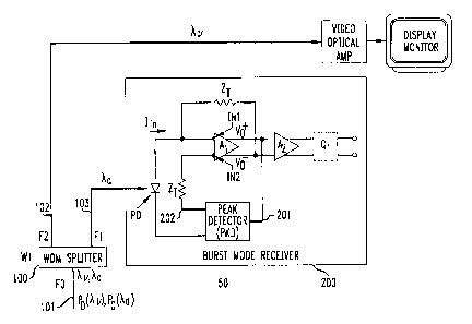
In a system where a second signal interferes with the detection of a first
signal at an input, in which the second signal is composed of a low frequency
component and a portion of the frequency spectrum that is higher than that of
the first signal, then both signals are processed to eliminate such interferenceby filtering the second signal to eliminate the portion of the frequency
spectrum that is higher than that of the first signal and eliminate the low
frequency component of the second signal. Advantageously, such processing is
done without affecting any low frequency component of the first signal.


French Abstract

Dans un système où un second signal brouille la détection d'un premier signal à une entrée et où ce second signal a une composante basse fréquence et une composante dont le spectre de fréquences est plus élevé que celui du premier signal, les deux signaux sont traités de façon à éliminer ce brouillage par filtrage du second signal pour supprimer la composante dont le spectre de fréquences est plus élevé que celui du premier signal et supprimer la composante basse fréquence du second signal. Ce traitement peut être effectué sans perturber les basses fréquences qui pourraient se trouver dans le premier signal.

Claims

Note: Claims are shown in the official language in which they were submitted.


Claims
1. A method of operating a digital data receiver having a high-degree
of immunity to a plurality of interfering signals, said method comprising the
steps of
receiving first and second signals at an input such that said second
signal interferes with detecting said first signal at the data receiver, said second
signal incorporating a low frequency component and also a portion of the
frequency spectrum that is higher than that of the first signal, and
filtering said second signal to eliminate said portion of the frequency
spectrum that is higher than that of the first signal and to eliminate said low
frequency component of said second signal without affecting any low
frequency component of the first signal.
2. The method of claim 1 wherein said first signal is derived from an
optical digital data signal and said second signal is derived from an optical
video signal, said method further comprising the steps of
connecting said input to an optical WDM splitter via a photodetector as
a way of receiving said first and second signals, said WDM splitter receiving
said optical data signal and said optical video signal via an optical fiber.
3. The method of claim 1 further comprising the steps of
generating an offset signal, and
canceling the low frequency component of said second signal by means
of the offset signal.

4. The method of claim 3 wherein said offset signal has a level
substantially equal to the level of said low frequency component of said second
signal.
5. A digital data receiver for selectively receiving a digital data signal
when the data signal is accompanied by a video signal having an amplitude
level exceeding the amplitude level of data signal, said receiver comprising
means for receiving said data and video signals at an input such that
said video signal interferes with detecting said data signal at the data receiver,
said video signal having a low frequency component and also a portion of the
frequency spectrum that is greater than that of the data signal, and
means for generating an offset signal, and
means for canceling by means of said offset signal only the low
frequency component of said video signal.
6. The receiver of claim 5 wherein said digital data signal is derived
from an optical data signal and said video signal is derived from an optical
video signal, said receiver further comprising
means for connecting said input to an optical WDM splitter via a
photodetector as a way of receiving said data and video signals, said WDM
splitter receiving said optical data signal and said optical video signal via anoptical fiber.
7. The receiver of claim 6 wherein said offset signal has a level
substantially equal to the level of said low frequency component of said video
signal.

Description

Note: Descriptions are shown in the official language in which they were submitted.


- 219b~39
Optical Wavelength Demultiplexer for a Video
Passive Optical Network
FIELD OF THE INVENTION
The invention relates to the demultiplexing of optical signals.
BACKGROUND OF THE INVENTION
An Optical Network Unit (ONU) that is arranged to receive multimedia
applications at an end-user location needs to include a demultiplexe~'to
separate 1.3 ~m wavelength digital data signals and 1.55 ~m wavelength video
signals from one another as they are received from a video-passive optical
network (V-PON) via a common optical fiber communications path. One
important criterion that needs to be met in performing such demultiplexing is
providing more than 40 dB of isolation between the optical signal is to keep
the
level of "cross-talk" between the demultiplexed optical signals to a minimum.
This multiplexing goal may be met by using a multistage WDM splitter
providing excellent isolation (> 45 dB) between 1.30~,m and 1.55~.m wavelength
signals or by using a single stage WDM splitter in combination with an optical
filter. Disadvantageously, such an approach is either too costly or its
insertion
loss is too high. Because of this, a purely optical approach to solving the
problem of "optical signal isolation" is not a good choice for use in an ONU.
SUMMARY OF THE INVENTION
We have recognized that the aforementioned required level of isolation
may be readily met by using a relatively inexpensive electrical approach
rather
than the more costly and purely optical approach of using a multistage WDM
optical splitter or a single stage optical splitter with an optical filter. In
a

2'96239
2
V-PON, the more stringent requirement is to prevent the 1.55~m video signal
from interfering with the proper detection of the 1.3~,m digital data signal.
We achieve this result by first recognizing that the interfering video
signal is a RF radio-frequency waveform having frequency components in the
high (RF) frequency domain as well as at low frequency near do (proportional
to the net average optical power of the interfering video signal).
Accordingly,
we deal with both the high frequency and low frequency components to
prevent them from interfering with the information carried in the digital
signal.
Specifically, the low frequency component of the interfering video signal may
be eliminated using a non-linear adaptive cancellation process that does not
interfere with the detection of the low frequency component of the digital
signal. Moreover, an RC time constant at a preamplifier input contained in the
canceler may be set so that it "filters out" the RF component of the
interfering
video signal, thereby effectively eliminating the interfering (unwanted) video
signal from the digital data stream.
The foregoing electrical approach thus significantly advances the art of
multiplexing optical signals when there is a strong need to provide a high
level
of isolation between multiplexed optical signals.
BRIEF DESCRIPTION OF THE DRAWING
FIG. 1 is a broad block diagram of an illustrative burst mode receiver;
FIG. 2A illustrates an optical signal of a particular power level and the
resulting photocurrent in burst mode communication;
FIG. 2B illustrates a signal recovered from the signal of FIG. 2A at the
output of an amplifier Al;

Z~9b239
3
FIG. 3 illustrates an offset voltage level, Vo~, that needs to be generated to
offset the effect of the interfering signal;
FIG. 4 is a broad block diagram of the burst mode receiver of FIG. 1
further arranged to adaptively generate the offset signal that cancels the
interfering signal;
FIG. 5A illustrates the case in which the incoming photocurrent shown
in FIG. 2A includes a digital data signal but does not include the interfering
video signal; and
FIG. 5B illustrates the case in which the incoming photocurrent shown in
FIG. 2A does include the interfering video signal.
DETAILED DESCRIPTION
In a Video-Passive Optical Network (V-PON), bursty digital data signals
and broadcast video signals may be transmitted simultaneously over an optical
fiber. This may be done using Wavelength Division Multiplexing (WDM) to
transmit simultaneously different optical signals having respective
wavelengths ~,~ (video) and ~,d (data) over the same optical fiber. Typically,
~,~
and ~,d are 1.55 ~.m and 1.3 Vim. Also, the video carrier frequency, f~, is
usually
much higher than the frequency range of the receiver that will receive the
digital data.
Thus, the digital data receiver must recover the bursty optical data
signal, and do so by neutralizing the interference resulting from the presence
of the optical video signal. We have recognized that a burst-mode receiver
having non-linear do cancellation may be used for such a purpose. One such
receiver is disclosed in our U. S. Patent 5,025,456 issued on June 18,1992,

CA 02196239 2001-02-28
4
entitled "Burst Mode Digital Data Receiver". Accordingly, the following is
discussed in the context of the referenced receiver. However, that should not
be
construed as a limitation, since it will be appreciated that other techniques
may
also be used to implement the principles of our invention.
Turning then to FIG. 1, ONLJ 50 includes WDM sputter 100 which
demultiplexes (separates) a video signal of wavelength ~,,, and digital data
signal
of wavelength ~ received via optical path 101 onto optical fiber paths 102 and
103, respectively. If WDM splitter 100 were "ideal" -- meaning that the
isolation
between the signals was infinite -- then the 1.55 ~m wavelength optical signal
would not be coupled to path 103, and, therefore would not interfere with
receiver
200. However, when the optical digital data is coupled to photodetector PD,
the
latter generates current I;" which is supplied to a first input of amplifier
Al.
Amplifier Al, in turn, converts that input current into voltage levels
(signal) V +,
Vo where Vo = V +. The voltage Vo+ is then stored in peak-detector PKD via
path 201. An output of PKD is supplied to a second input of amplifier AI via
path
202 and resistor ZT to establish an appropriate logic threshold, as is
illustrated in
FIGs. 2A and 2B. Specifically, FIG. 2A illustrates an optical signal having an
optical power of P(~) and photocurrent I~ . FIG. 2B, on the other hand,
illustrates a waveform of the differential recovered voltage signal Vo - Vo .
Peak-detector PKD, FIG. 1, operates, as will be discussed below, to generate a
threshold voltage VTH that is substantially equal to the voltage swing of Vo+
that is
equivalent to one-half of the maximum output signal swing. This condition may
be met if the isolation provided by WDM splitter 100 were infinite. However,
such isolation is typically 20 dB. Moreover, since the power of the
interfering
optical video signal supplied to splitter 100 could be approximately 10,000
times
(40 dB) greater than the power of the optical digital signal that is also
supplied to
splitter 100, then the optical power of the video signal that is coupled into
path

CA 02196239 2001-02-28
103 may be approximately 100 times (20 dB) greater than the optical power of
the
digital data signal (i.e., the larger 40 dB video optical signal is attenuated
20 dB
by the wavelength isolation of the splitter, thus becoming 40 dB - 20 dB = 20
dB
( 100 times) larger than the digital data signal).
If the video carrier frequency, f~, is much greater than the upper limit of
the
bandwidth range, BWd, of the digital receiver, then the receiver cannot
quickly
respond to a video signal modulated onto a carrier of f~. In that case,
digital
receiver 200 tends to filter the high-frequency components of the video signal
near f~, and outputs only the low-frequency average power signal of the
received
video signal defined herein as Io. Signal Io is translated to the output V +
of
amplifier A~ in the form of an offset voltage Vow illustrated in FIG. 3. As
noted
earlier, peak-detector PKG sets the logic threshold at one-half of the maximum
signal swing. It is seen from FIG. 3 that because VTH is located within Vow,
receiver 200 fails to detect the digital signal.
Accordingly, the offset voltage Vo~ that is caused by the video signal
coupled to path 103 needs to be removed (canceled) to detect the digital
signal.
One scheme that may be used to remove the unwanted signal is disclosed in our
U.S. Patent No. 5,371,736 issued December 6, 1994. A broad block diagram of
the circuit discussed in the '736 patent is shown in FIG. 4, which is actually
a
somewhat modified version of receiver 200, FIG. 1. Specifically, peak-detector
PKD, FIG. 1, is shown in FIG. 4 as a positive peak-detector P-PKD. FIG. 4 also
includes a negative peak-detector N-PKD.
If incoming photocurrent I;" does not contain low-frequency background
current, then the outputs, V + and Vo , of preamplifier A3 are symmetrical as

2'96239
6
shown in FIG. 5A. if, on the other hand, I;~ contains low-frequency background
current Io, then Vo+ and Vo are not symmetrical, as shown in FIG. 5B, and the
difference between their respective peaks is some value 0. This difference in
the signals, O, is stored in and supplied at the output of buffer B1 and is
low-
pass filtered by filter B2, FIG. 4, where it then controls the voltage
controlled
current source CS. Current source C5, in turn, subtracts the background
current
Io from the incoming photocurrent I;~ such that only the current, Id, due to
the
digital signal reaches the input of amplifier A3. In this way, the waveforms
of
FIG. 5B are modified to resemble the desired waveforms of FIG. 5A.
Accordingly, FIG. 4 operates, in accord with an aspect of the invention, to
cancel the low frequency component due to the interfering signal without
eliminating (canceling) the low frequency component due to the digital signal,
and, therefore, has a high-degree of immunity to interfering signals.
The foregoing is merely illustrative of the principles of the invention.
Those skilled in the art will be able to devise numerous arrangements, which,
although not explicitly shown or described herein, nevertheless embody those
principles that are within the spirit and scope of the invention.

Representative Drawing
A single figure which represents the drawing illustrating the invention.
Administrative Status

2024-08-01:As part of the Next Generation Patents (NGP) transition, the Canadian Patents Database (CPD) now contains a more detailed Event History, which replicates the Event Log of our new back-office solution.

Please note that "Inactive:" events refers to events no longer in use in our new back-office solution.

For a clearer understanding of the status of the application/patent presented on this page, the site Disclaimer , as well as the definitions for Patent , Event History , Maintenance Fee  and Payment History  should be consulted.

Event History

Description Date
Inactive: IPC expired 2013-01-01
Inactive: IPC from MCD 2006-03-12
Time Limit for Reversal Expired 2004-01-29
Letter Sent 2003-01-29
Grant by Issuance 2002-09-10
Inactive: Cover page published 2002-09-09
Pre-grant 2002-06-19
Inactive: Final fee received 2002-06-19
Notice of Allowance is Issued 2002-01-07
Letter Sent 2002-01-07
Notice of Allowance is Issued 2002-01-07
Inactive: Approved for allowance (AFA) 2001-12-18
Amendment Received - Voluntary Amendment 2001-11-09
Letter Sent 2001-10-05
Extension of Time for Taking Action Requirements Determined Compliant 2001-10-05
Extension of Time for Taking Action Request Received 2001-09-04
Inactive: S.30(2) Rules - Examiner requisition 2001-05-09
Amendment Received - Voluntary Amendment 2001-02-28
Inactive: Cover page published 2000-12-21
Inactive: S.30(2) Rules - Examiner requisition 2000-11-03
Inactive: Application prosecuted on TS as of Log entry date 1998-05-05
Inactive: Status info is complete as of Log entry date 1998-05-05
Application Published (Open to Public Inspection) 1997-09-22
Request for Examination Requirements Determined Compliant 1997-01-29
All Requirements for Examination Determined Compliant 1997-01-29

Abandonment History

There is no abandonment history.

Maintenance Fee

The last payment was received on 2001-12-28

Note : If the full payment has not been received on or before the date indicated, a further fee may be required which may be one of the following

  • the reinstatement fee;
  • the late payment fee; or
  • additional fee to reverse deemed expiry.

Patent fees are adjusted on the 1st of January every year. The amounts above are the current amounts if received by December 31 of the current year.
Please refer to the CIPO Patent Fees web page to see all current fee amounts.

Fee History

Fee Type Anniversary Year Due Date Paid Date
Request for examination - standard 1997-01-29
MF (application, 2nd anniv.) - standard 02 1999-01-29 1998-12-30
MF (application, 3rd anniv.) - standard 03 2000-01-31 1999-12-21
MF (application, 4th anniv.) - standard 04 2001-01-29 2000-12-20
Extension of time 2001-09-04
MF (application, 5th anniv.) - standard 05 2002-01-29 2001-12-28
Final fee - standard 2002-06-19
Owners on Record

Note: Records showing the ownership history in alphabetical order.

Current Owners on Record
LUCENT TECHNOLOGIES INC.
Past Owners on Record
ROBERT GERALD SWARTZ
YUSUKE OTA
Past Owners that do not appear in the "Owners on Record" listing will appear in other documentation within the application.
Documents

To view selected files, please enter reCAPTCHA code :


To view images, click a link in the Document Description column. To download the documents, select one or more checkboxes in the first column and then click the "Download Selected in PDF format (Zip Archive)" or the "Download Selected as Single PDF" button.

List of published and non-published patent-specific documents on the CPD .

If you have any difficulty accessing content, you can call the Client Service Centre at 1-866-997-1936 or send them an e-mail at CIPO Client Service Centre.


Document
Description 
Date
(yyyy-mm-dd) 
Number of pages   Size of Image (KB) 
Abstract 1997-05-06 1 18
Description 1997-05-06 6 248
Claims 1997-05-06 2 69
Drawings 1997-05-06 4 41
Description 2001-02-27 6 253
Representative drawing 2001-12-18 1 8
Representative drawing 2000-12-07 1 7
Representative drawing 1997-11-04 1 7
Reminder of maintenance fee due 1998-09-29 1 110
Commissioner's Notice - Application Found Allowable 2002-01-06 1 164
Maintenance Fee Notice 2003-02-25 1 174
Correspondence 2002-06-18 1 35
Correspondence 2001-09-03 1 30
Correspondence 2001-10-04 1 14