Note: Descriptions are shown in the official language in which they were submitted.
~ 2196~1~
CFO 11912
TRANSMISSION CONTROL METHOD IN NETWORK SYSTEM
FOR SIGNAL TRANSMISSION BY PLURAL CHANNELS
AND NETWORK SYSTEM 1 llhK~;l''U~C
5 BACKGROUND OF THE INVENTION
Field of the Invention
The present invention relates to a network system
and a trAne~ml c~1 ~)n control method, and more
particularly to a network system of a configuration
10 with plural node devices connected with plural
r.hAnn~ ~. More gpecifically it relates to a network
system of a configuration in which plural tl~rm1nAl
eguipments are respectively connected to the plural
~hF~nn~l ~ through each of the node devices.
15 Related Bavhyluulld Art
Recently active developments are conducted on the
network systems for effecting ~ 1 ration by
connecting plural t~r.min 1l eqlli, L~i, and there are
already known various configurations such as a bus-type
20 configuration in which the plural tF~rmlni~l eqlll L~i
are connected to a bus line, a ring-type configuration
in which the t~r.m.1n~l eglll, ~ L~i are connected to a
ring-shaped trAn~m1ccl~n path, and a star-type
cûnfiguration in which the t~rmln~l eglll, LY are
25 ~;vlllle-;L~d through active or passive couplers. Also for
increasing the tr~n~ n capacity, there i5 known a
multi-channel configuration in which node devices, to
which the t~r~m1ns~l egll1 LY are .,vlllle~,Lt:d, are
~ 2~96514
-- 2 --
connected with plural rh~nn~1o., Also a configuration
ut~lf71n~ hts of mutually different wavelengths as
the plural rh~nn~lo. and mulfirl~x~n~ such lights is
known as a wavelength-division-mul~1rlpx~fl network
5 system.
The present invention relates in particular to a
network system of a configuration in which the node
devices are ~vllne~ d with plural rhzlnn~lo.,
In the conventionally known network systems
10 ut1li7in~ plural rh~nn~lo., a large switching device has
to be employed for the trAnom~ ~R~ nn control of the
signals, in order to process the signals transmitted in
the plural r.h~nn~l F~,
An ob~ ect of the present invention is to provide a
15 network system and a trnnPm~ )n control method,
fAcilitating such control.
SUMMARY OF THE INVENTION
Prior to the explanatlon o~ the configuration of
20 the present invention, there will be ~xrl~n~-l, as a
reference example, the configuration disclosed in the
Japanese Patent Laid-open Application No. 8-237306.
Referring to Figs. 16A and 16B, a control unit 93
for the node devices of this reference example is
25 provided therein with a buffer control unit 94 and a
wavelength control unit 5 . The buf fer control unit 94
is provided with a buffer reading control unit 3 for
effecting the read control of the buffer, in case a sub
2196~1L1
~-- - 3 -
tr~n~ i nn path used for the destination of
tr~nrm i ~8 i nn of a paoket stored in the buf fer is
connected to an ad~acent node device, 80 as not to read
such packet from the buffer until the wavelength
5 received by a fixed wavelength receiving unit of the
ad~ acent node device which is adapted to output the
packet to a separation-insertion unit to which the sub
tr;~n~m i q8 i nn path of the destination is connected
~ol nr i flDS~ wlth a tr~n~ ' cs i nn wavelength of a variable
lO wavelength transmitting unit for transmitting such
packet in the ad~ acent node device . The wavelength
control unit 5 controls the trF~n~m i c~ i nn wavelength of
the variable wavelength transmitting means according to
the pattern of a plt:de~.-.,, in~ri tr~nPmi~inn wavelength
15 control table to be P-rrl~in~d later. An optical fiber
6 thilt i8 an optical wavelength division mUlt i rl D- 'i n5j
trAn~ i nn path serves as a tr~n~ i nn path between
a wavelength multiplexer of an upstream ad'jacent node
device and a divider of the local ( self ) node device.
20 A divider 7 divides optical signals transmitted through
the optical f iber 6 and sends them to seven f ixed
wavelength receiving units. Numerals 8 to 14 indicate
fixed wavelength receiving units I - VII constituting
f ixed wavelength receiving means, each of which is
25 ,~ ' of an optical filter of a fixed wavelength and
a photodiode, and each of which only receives a packet
of optical signals with one of wavelengths ~1 to ~7.
Numerals 15 to 21 indicate separation-insertion units
~ 2196Sl~
-- 4 --
I - VII constituting separation-insertion means, which
serve to separate a packet flow from the fixed
wavelength receiving units 8 - 14 into packets to be
transmitted to respective sub trRnrm~ ~rl on paths and
5 those to be sent to the buffers, and to insert packets,
transmltted from the respective sub trRnrm~ r)n paths,
into the packet flow supplied from the fixed wavelength
receiving units 8 - 14 to the buffers. Numerals 95 -
101 indicate buffers I - VII constitutlng buffer means
10 and serving to temporarily storing the packets,
released from the separation-insertion units 15 - 21,
in memory regions respectively corresponding to the
trRnrm~ ~Rl ~n wavelengths of the variable wavelength
transmlttlng unlts. Numerals 29 - 35 lndlcate varlable
15 wavelength transmittlng unlts I - VII constltutlng
varlable wavelength transmitting means utilizing
tunable laser diodes ( TLD ) and serving to convert the
packets, released from the buffer units 95 - 101, into
optical slgnals of pLI:det~- lnPA wavelengths among the
20 wavelengths ~ 7 under the control of the wavelength
control unit 5, for trRn~ rn through a wavelength
multlplexer 36 to an optical flber 37 constltutlng an
optlcal wavelength division mult1rlF~Yln~ trRnrm~ n
path. In the present em~bodiment, the fixed wavelength
25 receivin~ unit I 8, the ~ p~Lz-Lion-insertion unit I 15,
the buffer I 95 and the variable wavelength
transmltting unit I 29 are, ' ~n/~l as a set, and the
~~ 219651~
-- 5 --
packet received in the fixed wavelength receiving unit
I 8 is processed only in this set. Similarly the fixed
wavelength receiving unit II 9, the separation-
insertion unit II 16, the buffer II 96 and the variable
5 wavelength transmitting unit II 30 are ~ nP~l as a
set, and other fixed wavelength receiving units,
separatlon-lnsertlon unlts, buffers and varlable
wavelength transmlttlng unlts are also ~ ' ~nPd
slmilarly. A wavelength multiplexer 36 mul~lrlPY~R the
10 optical signals of wavelengths ~ 7 released from
the seven varlable wavelength transmitting units, and
emits the multiplexed optical signal to the optical
fiber 37. The optlcal flber 37, constltuting an
optical wavelength divlslon mult~ rl PYi n~ tr; ln pm 1 C:P~ ~ nn
15 path, serves as the trAn~ q~ r~n path between the
wavelength multlplexer 36 of the local (self) node
device and the dlvlder 37 of the downstream ad~ acent
node device. Numerals 38 ~ 44 are sub tr~lr ' ~F~l on
paths I - VII servlng as packet tr~n~m~qq~n paths
20 between the separation-insertion unlts 15 - 21 and
tPrmtnq7 equlpment. Numeralg 45 - 51 indlcate tPr,mln;~l
eq~ VII Lt~e~i~lvely connected to the sub
tr;~nPmlcq~n paths I 38 - VII 44, servlng to recelve
the packets released from the separation-lnsertion
25 unlts 15 - 21, and to prepare packets to be transmltted
to other tPrm~n~l eqll~ and to transmlt them to
the separation-insertion units 15 - 21 through the sub
~ 2196514
-- 6 --
transmission paths 38 - 44.
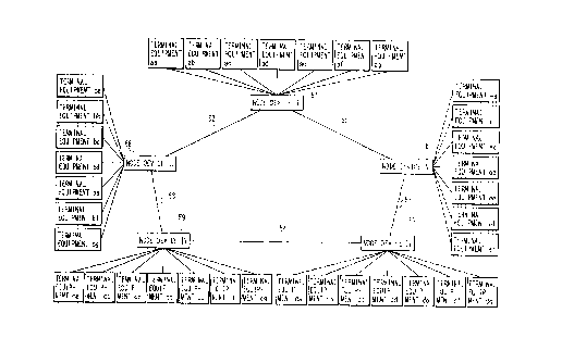
Fig. 2 shows an example of configuratlon of a
network system ut~li7in~ the node devlces shown in
Flgs. 16A and 16B, whereln flve node devices are
5 connected through optical fibers. Numerals 57 - 61
indicate node devlces shown in Figs. 16A and 16EI, each
of which is connected to seven terminal eSIuipments
through seven sub trnnrm~ RR~ nn paths . Numerals 52 - 56
indicate optical fibers constitutlng the optlcal
10 wavelength division mult~r~xin~ tr~nFmlRR~-n paths.
Fig. 17 shows the internal configuration of the
buffers I 95 - VII 101 employed in the node devices.
The buffers I - VII have an identical internal
configuration. In Fig. 17, a decoder 102 reads an
15 address portion of the input packet, discriminates
whether the destination of the packet iB a sub
trnn~ m~RRI~m path connected to an adjacent node device,
and, if not, lnstructs a demultiplexer 105 80 as to
direct the output thereof to an FIFO 107. On the other
20 hand, lf the destination of the packet is a sub
trnn1mlRRIol~ path connected to the adjacent node
device, the decoder 102 lnstructs the demultlplexer 105
so as to direct the output thereof to a dual-port
memory 106 and instructs a write address counter 103 of
25 a write start address of a memory region nRsl~n~rl to
the packet.
A write address counter 103 supplies the dual port
2196al~
-- 7 --
memory 106 with identification signals of the memory
regions in which the packets are to be written, in
sllr:n~Qq1 r~n from the write start address released from
the decoder 102. ~he memory region of the dual port
5 memory 106, where the packet is to be stored, is
related with the destlnation terminal equipment of the
packet. For example, in case the packet destination is
a t~rm1nAl e~uipment II 46 uu~ euL~:d to the ad~acent
node device, in order that the packet can reach such
10 ~rmf nAl e~auipment II 46 which i9 connected to the
s~alelLlon-insertion unit II 16, the packet has to be
entered as the optical signal of wavelength ~2 in the
f ixed wavelength receiving unit I I 9 connected to the
separation-insertion unit II 16 in the node device, and
15 for conversion into the optical signal of wavelength
~2, the packet has to be stored in the memory region II
in the dual port memory 106.
A read address counter 104 ~q--rrl ~Pq the dual port
memory 106 with address signals for reading the
20 packets, in sllnnF~qq1rm starting from a read start
address L~ lLt:d by an offset value released from
the buffer reading control unit 3.
A demultiplexer 105 sends the input packet either
to the dual port memory 106 or to the FIFû 107,
25 according to the instruction from the decoder 102. ~he
dual port memory 106 is provided for effecting the
writing and the readlng of the packet data in mutually
~ 2196~14
-- 8 --
indep3lldell1, manner, and is provided with memory regions
in such a manner that the trAnFm1qqlrn packets
correspond to the wavelengths of the optical signals to
be l~ llVt:l ~ed. For example, a packet stored in a memory
5 region IV i8 read only when the trAn~ qC1 ~n wavelength
of the variable wavelength transmitting unit is set at
the wavelength ~4, and is transmitted thereby as the
optical signal of wavelength ~4. The packet stored in
each memory region is ~JIIV~l l,ed into the optical signal
10 of a wavelength corrPsp~n~l~n!J to each memory region and
released from the node device. The head addresses of
the memory regions I - VII are respectively A1, A2, A3,
A4, A5, A6 and A7.
An FIF0 (first-in-first-out) register 107
15 temporarily stores the input packets and releases them
in the order of input to a selector 108, which connects
either one of output tPrm1nAlq of the dual port memory
106 and the FIF0 107 to the variable wavelength
transmitting unit according to the in~lu.d,Lon from the
20 buffer reading control unit 3.
Fig. 5 shows the configuration of the buffer
reading control unit 3 in the buffer control unit 94,
wherein numerals 76 - 82 indicate buffer control tables
I - VII, which are read in s~ PRqi~n by the addresses
25 released from the wavelength control unit 5 nnd send
the read predetPrm~nPfl offset values to a read address
counter 104 for the buffers I - VII. These tables are
~ 2196al4
g
composed of read-only memories (ROM), and have contents
to be Pxrl~lnP~ later. A reading control unit 83 sends
a read control slgnal, for readlng the packet elther
from the dual port memory 106 or from the FIF0 107, to
5 the buffers I 95 - VII 101, by counting clock signals
released from the wavelength control unlt.
Fig.7 shows the internal configuration of the
wavelength control unit 5, wherein numerals 85 - 91
indicate wavelength control tables I - VI I, which are
10 read in ~ ('P~::C~r~n by the addresses released from a ROM
counter 84 to send predetPrm1nPd wavelength control
signals to a drive unit of the variable wavelength
transmltting unit. These wavelength control tables are
composed of a read-only memory ( ROM ) and have contents
15 to be ~Yr]~nPtl later. A clock generator 92 generates
a ~ledel~ nPd clock slgnal for supply to the buffer
control unit, and divldes the frequency of the clock
signal, for supply to the ROM counter.
The ~;ull~ellL~ of the abovc ~loned wavelength
20 control tables I - VII indicate the transition of the
wavelengths of the optical signals transmitted by the
variable wavelength transmitting unit, and are set, as
an example, as shown ln Table 1, whereln numerals 1 - 7
respectively stand for the wavelengths ~ 7.
~ 21g~14
-- 10 --
Table 1
Address 0 1 2 3 4 5 6
Table name ~
Wavelength control table I 1 3 5 7 6 4 2
5 Wavelength control table II 3 5 7 6 4 2
Wavelength control table III 5 7 6 4 2 1 3
Wavelength control table IV 7 6 4 2 1 3 5
Wavelength control table V 6 4 2 1 3 5 7
Wavelength control table VI 4 2 1 3 5 7 6
10 ~avelength control table VII 2 1 3 5 7 6 4
Also the offset values ~;ulLt~ ~ding to the
address value in the aLur~ Lloned buffer control
tables I - VII are set as shown in Table 2.
15Table 2
~ __ Addres3 0 1 2 3 4 5 6
Table name \
Buffer control table I Al A3 A5 A7 A6 A4 A2
Buffer control table II A3 A5 A7 A6 A4 A2 Al
20Buffer control table III A5 A7 A6 A4 A2 A1 A3
Buffer control table IV A7 A6 A4 A2 Al A3 A5
Buffer control table V A6 A4 A2 A1 A3 A5 A7
Buffer control table VI A4 A2 A1 A3 A5 A7 A6
Buffer control table VII A2 Al A3 A5 A7 A6 A4
These wavelength control tables and buffer control
tables, Lou~ en in total number, are read ln
~ 2196~14
-- 11 --
synchronlzatlon by the ROM counter 84, whereby the
trAnFm1 cc1 nn wavelength of each tunable laser diode
(TLD) is cyclically shifted in the order of ~ 3, ~5,
7~,7, ~6, ~4, ~2, 1~l,..., and the offset value for
5 reading the memory region in the dual port memory of
the buffer connected to each tunable laser diode
synchronized with this transition is also cyclically
shifted in the order of Al, A3, A5, A7, A6, A4, A2,
Al,... Thus, according to these wavelength control
10 tables and the buffer control tables, the packet in the
memory region ~,oLl~2,~ol~ding to the cyclically shifted
trAn~ m1 Cc1 nn wavelength of the variable wavelength
transmitting unit is released 80 as to be l,:~JllV~U l,ed
into an optical signal of the current trAnFm1 cc1 nn
15 wavelength of the variable wavelength transmitting
unit. The cyclic trangitions of the tr~n m1 ccf nn
wavelength of the tunable laser diodes are mutually
shifted in phase, in order that the 1,1 cq1 nn in a
given wavelength is not simultAnpm~cly c~ du.~ d by
20 plural tunable laser diodeg. The trAnl 'cclr)n
wavelength of the variable wavelength transmitting
units are controlled by the wavelength control tables I
- VII set in the above-~YrlA1n~d manner.
In the following there will be ~YplA1n~ the
25 tr~nFm1cF~nn control method of the present network
system, with reference to Figs. 2, 4, 5, 7, 16A and
16B, and 17, Tables 1 and 2, and timing charts in Figs.
219~51~
-- 12 --
8, 9, 10, 18, 19 and 20. The operation times shown in
Figs. 8, 9, 10, 18, 19 and 20 are common in these
timing charts. For example, an operation T3 in Fig. 8
is same as that in Fig. 9.
Now the function of the trFIn-'m1 c51 nn control
method is PYrl~1n~tl by an example of tr~ne~m1p~p~lnn of a
packet dispatched from a f~rm1n~l equipment I 45,
connected to the sub tr~n~ 81 Qn path I 38 of the node
device I 57, and having the destination at a ~-~rm1n;11
equipment II 46 connected to the sub tr~n~m1 P.8~ nn path
II 39 of the node device V 61. In the following there
will be ~Yrl~n~ the tr~nPm~ on of three packets A,
B and C. For the purpose of clarity, equivalent
components in the different node devices are
represented by same numbers as those in Figs. 4, 5, 7,
16A and 16B, and 17.
The operations of the node devices I 57 - V 61 at
different operation times will be ~~Yrl~1n(~fl with
respective L~e~ c,a to Figs. 9, 10, 18, 19 and 20.
Also it is assumed that the ~ddl~sses ( sync signals )
~rom the ROM counter 84 for reading the buffer control
tables and the wavelength control tables in the node
device are ~ntlF~rpn~nt in each node device, as shown in
Fig. 8. Thus the read address values from the ROM
counter 84 of the wavelength control unit 5 is
displaced in phase, among the different node devices.
Also these address values are given in Fig. 8 only for
2196~14
-- 13 --
periods corrf~p~nn(l ~ n~ to the operation times of the
packet relaying functions of the different node devices
in the relevant drawings and are omltted in other
periods. For example, in this reference example, the
5 packet relaying operation of the node device II 58 is
P.q~lAln~cl in a period from an operation time T3 to an
operation time T7 in Fig. 9, 80 that the address values
for the node device II 58 in Fig. 8 are given only in a
UUlL'-~L" ~ 1 n~ period.
In the following there will be ~plAln~l the
1 rAting operation of the node device I 57 with
referenoe to Fig. 9. At the start of an operation time
Tl, the tc~rmln~l equipment I 45 uull-leu~d to the sub
trAn~ml ePi~ n path I 38 of the source node device I 57
15 adds, to the trAn~mlPPlnn data, the address of the
tr~rmlnAl equipment II 46 connected to the sub
trAnrmlPrl-m path II 39 of the destination node device
V 61, and releases a packet A through the sub
trAnom~pl~n path I 38 to the separation-insertion unit
20 I 15 of the node device I 57.
In the operation time Tl, the separation-insertion
unit I 15 of the node device I 57 finds a gap in the
packet flow received by the fixed wavelength receivlng
unit I 8, and sends the packet A, entered through the
25 sub trAnPmlppl~n path I 38, to the buffer I 95 by
inserting the packet A into such gap. In the operation
time Tl, the decoder 102 of the buffer I 95 reads the
~ 2196~1~
-- 14 --
address portion of the entered packet A. Since the
destination of the packet A ls not the tPr.mlnAl
eq~ ~u~ e~ e~ to the adj acent node device II 58,
the decoder 102 directs the output of the demultiplexer
105 to the FIFO 107, whereby the packet A is wrltten
therein .
In an operation time T2, the separation-insertion
unit I 15 of the node device I 57 finds a gap in the
packet flow received by the fixed wavelength receiving
unit I 8, and sends a packet B, entered through the sub
tr lnrml ~ nn path I 38, to the buffer I 95 by inserting
the packet B into such gap. In the operation time T2,
the decoder 102 of the buffer I 95 reads the address
portion of the entered packet B. Since the destination
of the packet B is not the tPrm. ln~l equipments
connected to the ad~acent node device II 58, the
decoder 102 directs the output of the demultiplexer 105
to the FIFO 107 whereby the packet B is written
therein .
In the operation time T2, the ROM counter 84 of
the wavelength control unit 5 sends a read address
value 1 simultAnpollcly to the wavelength control tables
I 85 - VII 91 (cf. Fig. 8), for reading the contents of
the wavelength control tables. In this content
reading, as shown in Table 1, the wavelength control
tables I, II, III, IV, V, VI and VII respectively
provide control signals corrP~pnn~n~ to wavelengths
~~ 21~6~1~
-- 15 --
~3, ~5, ~7, ~6, ~4, ~2 and ~1. These control signals
are respectlvely supplied to the variable wavelength
transmitting units I 29 - VII 35, which in response
emit optical signals of predetPrm1 n~fl wavelengths .
The read address value 1 from the ROM counter 84
of the wavelength control unit 5 is also supplied to
the buffer control tables I - VII of the buffer control
unlt 94, for readlng the ~_:Ulll.l~ i of the buffer control
5 tables. In this content reading, as shown in Table 2,
the buffer control tables I, II, III, IV, V, VI and VII
respectively provide offset values A3, A5, A7, A6, A4,
A2 and Al respectively corresponding to the memory
regions III, V, VII, VI, IV, II and I. These offset
lû values are respectively supplied to the read address
counters 104 of the buffers I 95 - VII 101.
Also in the operation time T2, the read control
unit 83 of the buffer control unit 94 provides, based
on the clock signal released from the wavelength
15 control unit 5, the selector 108 with a control signal
for Pn~hl1n~ the reading of the dual port memory 106
and Als~hlln~ the reading of the FIFO 107 in a
predet~rml nPA dual port memory reading time Td within
the operation time T2, and then provides the selector
20 108 with a control signal for Pn~ihl ln3 the reading of
the FIFO 107 and Al~ hl ln~ the reading of the dual port
memory 106 in a ~Lt:d,~ nPA FIFO reading time Tf =~
(= T - Td). Thus the input tPrm~n~l of the selector
219~514
-- 16 --
108 is connected to elther one of the FIF0 107 and the
dual port memory 106.
In the dual port memory reading time Td within the
operation time T2, the read address counter 104 in the
5 buffer I 95 generates, for supply to the dual port
memory 106, an address for reading the packet written
in the memory region III, by loading the offset value
A3 released from the buffer control table I 76 and by
sllr.r~Q~ve in~ i of the count. In response to
10 this read address, a packet is read from the cutput
port of the dual port memory 106 and is supplied to the
variable wavelength transmitting unit I 29. Since no
packet storeds in the memory region III of the buffer I
95 in the operation time T2, no packet is supplied to
15 the variable wavelength transmitting unit I 29.
In this e_ample, however, for the purpose of
understanding, there will be PYrl~1n~t9 a case of
reading only one packet in the times Td and Tf.
In the FIF0 reading time Tf (= operation time T -
20 Td ) within the operation time T2, the read control unit83 in the buf fer reading control unit 3 sends a control
signal, for ~n~hl ~n~ the reading of the FIF0 107 and
~1QAhl1ng the reading of the dual port memory 106, to
the selector 108, which in response sends the packet A,
25 stored in the FIF0 107, to the variable wavelength
transmitting unit I 29. Since the tr;ln IQQ1rn
wavelength of each variable wavelength transmitting
~ 2196~14
-- 17 --
unit is constant within each operation time T,
regardless of the time Tf or Td, the packet A is
UUIIV.21 Led into an optical signal of wavelength ~3 by
the variable wavelength transmitting unit I 29 and
5 supplied to the wavelength multiplexer 36.
Also the variable wavelength transmitting units II
30 - VII 35 respectively convert the packets released
from the buffers II 96 - VII lOl into optical signals
of predetorm1nPtl wavelength, based on the wavelength
10 control signal from the wavelength control unit 5 and
sends these optical signals to the wavelength
multiplexer 36. As P--rlA~nP~ in the foregoing, the
optical signals released from the variable wavelength
transmitting units II 30, III 31, IV 32, V 33, VI 34
and VII 35 respectively have wavelengths ~5, ~7, ~6,
~4, 7~.2, and ~1. Since the optical signals released
from the seven variable wavelength transmitting unlts
have mutually different wavelengths under the control
of the wavelength control unit 5, these optlcal signals
20 are mlxed wlthout mutual lllLe:Lrel~llce ln the wavelength
mult~rlP~or 36, whereby the lights of all the
wavelengths enter the optical fiber 37 and are
transmitted to the du...lxLl~ adjacent node device II
58 .
In an operation time T3, a packet C ls inserted
into the packet flow in the separation-lnsertion unit I
15, and ls stored ln the FIF0 107 ln the buffer I 95 ln
~ 2196514
-- 18 --
the same manner as the packet B.
In the operation time T3, the packet is read from
the buffer and transmitted in the following manner. A
read address value 2 ( cf . Fig . 8 ) is supplied from the
5 ROM counter 84 of the wavelength control unit 5,
simultaneously to the wavelength control tables I - VII
for reading the ~;u~ n~i thereof. The tr~nFmi~ n
wavelength of the variable wavelength transmitting unit
I 29 i~ set at ~5.
In the dual port memory read time Td within the
operation time T3, the read address counter 104 of the
buffer I 95 loads the offset value A5 released from the
buffer control table I 76 and generates an address for
reading the packet written in the memory region V, for
15 supply to the dual port memory 106. According to the
read address, the packet is read from the output port
of the dual port memory 106 and supplied to the
variable wavelength transmitting unit I 29, but, in the
operation time T3, since the memory region V does not
20 store any packet, the variable wavelength transmitting
unit I 29 does not receive any packet.
In the FIFO read time Tf ( = operation time T - Td )
within the operation time T3, the read control unit 83
sends the control signal, for ~n;qhl ~ ng the reading of
25 the FIFO 107 and ~ hl ~ n3 the reading of the dual port
memory 106, to the selector 108, which in response
sends the packet B, stored in the FIFO 107, to the
~ 219~
-- 19 --
varlable wavelength transmitting unit I 29. The packet
B ls ( :UIIV~l l,~d in the variable wavelength transmitting
unit I 29 into an optical signal of a wavelength ?,,5 and
supplied to the wavelength multiplexer 36. However the
tr~nr~ R1 ~)n wavelength of each variable wavelength
transmitting unit is constant within the operation time
T, regardless of the time Tf or Td.
The packet C in an operation time T4 is similarly
read from the FIFû 107 of the buffer I 95, supplied to
the selector 108, then ~.iUIIV~ d by the variable
wavelength transmitting unit I 29 into an optical
signal of ~7 and supplied to the wavelength multiplexer
36 .
Consesluently, the packets A, B and C are released
from the node device I 57 to the optical fiber 37,
respectively in the wavelengths ~3, ~5, and ~7 in the
operation times T2, T3 and T4. It is assumed that thus
released packets A, B and C are respectively received,
in the operation times T3, T4 and T5, by the f ixed
wavelength reoeiving units III 10, V 12 and VII 14 in
the node device II 58.
The timing chart showing the function of each node
device only shows the UUllt _ 1 Ated operations and the
1- ~n~ng parts are left blank. For example, Fig. 9
shows the trAn~ ' RR~ ~n wavelengths of the variable
wavelength transmitting unit I in the operation times
T2, T3 and T4, but the unit I emits the optical signal
~ 219651~
-- 20 --
of wavelength ~1 in the operation time I also.
In the following there will be P~rpl~lnPfl the
functlon of the node device II 58 with reference to
Fig. 10. In the operation time T3, the fixed
wavelength receiving unit III 10 receives the packet A
by the optical signal of ~3. The packet A is
transmitted by the separation-insertion unit III 17 and
ls supplied to the buffer III 97, in which the decoder
102 reads the address portion of the input packet A,
and, as the destination of the packet A ig not ~ nAl
eq-l~ L:j connected to the adJacent node device III
59, directs the output of the demultiplexer 105 to the
FIF0 107. The packet A is switched by the
demultiplexer 105 and stored in the FIF0 107 of the
buffer III 97.
In an operation time T4, the fixed wavelength
receivlng unit V 12 receives the packet B by the
optical signal of 1~ 5 . The packet B is transmitted by
the separation-insertion unit V 19 and is ~lrPl iP~l to
the buffer V 99, in which the decoder 102 reads the
address portion of the input packet B, and, as the
destination of the packet B is not any tPrnli n;~ 1
eq~ u~ eul t:d to the adJacent node device III 59
and it need not be released by designating the channel
or the wavelength, directs the output of the
demultiplexer 105 to the FIFû 107.
Also in the operation time T4, a read address
~ 2190514
-- 21 --
value 0 released from the ROM counter 84 of the
wavelength control unit 5 ( cf . Flg . 8 ) sets the
trl~n~ sl rln wavelengths of the varlable wavelength
transmitting units III, V and VII respectively at ~5,
5 ~6 and ~2. In the FIFO read time Tf (= operation time
T - Td) within the operation time T4, the read control
unit 83 sends the oontrol signal, for enabling the
reading of the FIFO 107 and A1~;~hllng the reading of
the dual port memory 106, to the selector 108, which ln
10 response sends the packet A stored in the FIFO 107 to
the variable wavelength transmitting unit III 31. The
packet A i9 ~;IJIIV~L ~d by the variable wavelength
transmitting unit III 31 into an optioal signal of
wavelength ~5 lmd supplied to the wavelength
15 multiplexer 36.
In an operatlon time T5, the fixed wavelength
receiving unit VII 14 receives the packet C of the
optical slgnal of ~7. The packet C i8 stored, like the
packet B in the FIFO 107 of the buffer VII 10. Also
20 the packet B is supplied, by the variable wavelength
transmitting unit V 33, as an optical signal of ~4 to
the node device I I I 5 9 .
In an operation time T6, the packet C is supplied,
by the variable wavelength transmitting unit VII 35, as
25 an optical signal of ~3 to the node device III 59.
In the following there will be P-'rl~nPA the
function of the node device III 59 with L~LeL~Ct~ to
~ 219~51~
-- 22 --
Fig. 11. It ls assumed that the packets A, B and C are
respectively received, in operation times T5, T6 and
T7, by the fixed wavelength receiving units V 12, IV 11
and III 10 in the node device III 57.
In an operation time T5, the fixed wavelength
receiving unit V 12 receives the packet A of the
optical signal of ~5. The packet A is transmitted by
the separation-insertion unit V 19 and is applied to
the buffer V 99, in which the decoder 102 reads the
address portion of the input packet A, and, as the
destination of the packet A is not any l~ n~
eqll~, I,s connected to the ad~acent node device IV 60,
directs the output of the demultiplexer 105 to the FIFO
107. The packet A is stored in the FIFO 107 of the
buffer V 99.
In an operation time T6, the packet B is received
by the fixed wavelength receiving unit IV 11, and is
stored in the FIFO 107 of the buf fer IV 98 . Also in
the operation time T6, ~ read address value 4 released
from the ROM counter 84 of the wavelength control unit
5 controls the variable wavelength transmitting unit V
33 80 as to emit the optical signal of wavelength ~3 in
the operatlon time T6, and in the FIFO read time Tf
( = operation time T - Td ) thereof, the packet A is
sl~ppl ~ P~9 by the varlable wavelength transmittlng unit V
33 as an optical signal of ~3 to the node device IV 60.
In an operation time T7, the packet C is received
~ 21~14
-- 23 --
by the fixed wavelength recelving unit III 10, and is
stored in the FIF0 107 of the buffer III 97. Also in
the operation time T7, the packet B is supplied by the
variable wavelength transmitting unit IV 32 as an
5 optical signal of ~3 to the node device IV 60, ana, in
an operation time T8, the packet C is supplied by the
variable wavelength transmitting unit III 31 as an
optical signal of ~3 to the node device IV 60.
In the following there will be ~pl~nPd the
10 function of the node device IV 60 with reference to
Fig. 19. The packets A, B and C are respectively
received, in operation times T7, T8 and T9, by the
fixed wavelength receiving unit III 10 in the node
device IV 60.
In the operation time T7, the packet A of the
optical signal of wavelength ~3 is received by the
fixed wavelength recelvlng unit III 10 and supplied to
the buffer III 97, in which the decoder 102 reads the
address portion of the input packet A. As the
20 destination of the packet A is the tf~ ni~l II 46
connected to the ad~acent node device V 61, the decoder
102 directs the output of the demultiplexer 105 to the
dual port memory 106 and sends a pLt:de~ n~-q write
start address A2 for the packet A to the write address
25 counter 103, which in response supplies the dual port
memory 106 with identification signal of the write
start address of the memory region, from which the
~-- 219651~
-- 24 --
packet A ls to be written. The packet A i8 stored in
the memory region II in the dual port memory 106,
because the packet A is addressed to the t~rmin~l II 46
connected to the node device V 61 and it has to be
5 UUllV.dL L~d into an optical signal of 7~,2 and supplied to
the fixed wavelength receiving unit II 9 connected to
the separation-insertion unit II 16 of the node device
V 61 in order that the packet A can reach the t~rm~n~l
II 46, as it 18 connected to the abov~ Lloned
10 separation-insertion unit II 16. The packet stored in
the memory region II of the dual port memory 106 is
read only when the tr~n~ml q~ n wavelength of the
variable wavelength transmitting unit is controlled to
~2, the packet A is thus ~;UlIVt:L L~d into an optical
15 signal of ~2 and released to the node device V 61.
In the operation time T8, the fi~ed wavelength
receiving unit III 10 receives the packet B as the
optical signal of ~3 and sends it to the buffer III 97,
in which the decoder 102 reads the address portion of
20 the input packet B. Since the destination of the
packet B i8 the terminal II 46 connected to the
adjacent node device V 61, the packet B is also stored
in the memory region II of the dual port memory 106.
Alxo in the operation time T8, the ROM counter 84
25 of the wavelength control unit 5 sends a read address
value 4 simult~n~o~ y to the wavelength control tables
- VII ( cf . Fig . 8 ) . This address v~lue reads the
~ 219~
-- 25 --
~:ullLel~ of the wavelength control tables, and the
wavelength control table III 87 sends a control signal
corresponding to the wavelength ~2 to the varlable
wavelength transmitting unit III 31, of which
5 tr~nPmlRs1~n wavelength is therefore set at ~2. In the
dual port memory read time Td within the operation time
T8, the read control unit 83 of the buffer reading
control unit 3 sends the control signal, for the
reading of the dual port memory 106 and disabling the
reading of the FIF0 107, to the selector 108, which in
response connects the dual port memory 106 with the
variable wavelength transmitting unit III 31. Also in
response to the read address value 4 from the ROM
counter 84 of the wavelength control unit 5, the buffer
15 control tables read the read address value in the
respective dual port memories and send them to the
address counter 104 . For example the buf fer control
table III 78, in response to the read address value 4
from the ROM counter 84 of the wavelength control unit
20 5, reads the head address A2 of the memory region II
and sends it to the address counter 104. Thus the dual
port memory 106 sends the paoket A to the variable
wavelength transmitting unit III 31, by which the
packet A 18 C.,llvt:L ~t:d lnto an optical signal of ~2 and
25 supplied to the wavelength multlplexer 36.
In an operation time T9, the flxed wavelength
receiving unit III 10 of the node device IV 60 receives
~ 219~51~
-- 26 --
the packet C as the optical signal of ~3. The packet C
is stored in the memory region II of the dual port
memory 106 .
In the operation time T9, the variable wavelength
5 transmitting unit III 31 is set at a tr;lnC~m~qq~nn
wavelength ~1 by a read address value 5 from the ROM
counter 84 of the wavelength control unit 5 ( cf . Fig .
8 ), and is therefore unable to transmit the packet B
stored in the memory region II 70 in the dual port
10 memory. Conse~auently, during operation times T10, Tll,
T12, T13 and T14 in which the variable wavelength
transmitting unit III 31 is set respectively at ),,3, ~5,
~7, ~6 and 1~,4, the packets 13 and C stored in the memory
region II of the dual port memory 106 are not CU1lV~ L~d
15 by the variable wavelength transmitting unit III 31
into the optical signal of wavelength oi ~2.
In an operation tlme T15, the variable wavelength
transmitting unit III 31 is set at wavelength ~2,
whereby the packet B stored in the memory region II of
20 the dual port memory is ~.:UIIVe:l L~d by the variable
wavelength transmitting unit III 31 into an optical
signal of ~2 and transmitted to-the wavelength
multiplexer 36. After the lapse of operation times
T16, T17, T18, T19, T20 and T21, the variable
25 wavelength transmitting unit III 31 is set in an
operation time T22 at the tr~nFmiqqlnn wavelength ~2,
h~llel t:UlJUII the packet C stored in the memory region I I
~-- 2196~1~
-- 27 --
of the dual port memory 106 is ~iUllV~ d thereby into
an optical signal of ~2 and transmitted to the
wavelength multiplexer 36.
In the following there will be explained the
5 function of the node device V 61, with reference to
Fig. 20. It is assumed that the packets A, B and C are
received by the fixed wavelength receiving unit II 9 of
the node V 61, respectively in operation times T9, T16
and T23.
The packet A, received in the operation time T9,
i8 ~al<~ d by the separatlon-lnsertlon unlt II 16
from the packets to be transmitted to the buffer II 96,
and 3upplied to the destinatlon tc~rm~n~l II 46.
Slmilarly the packet B, received in the operation time
T16 is ~ d from the packets to be transmitted to
the buffer II 96, ~nd supplied to the destination
t~rm1n~1 II 46. Also the packet C, received in the
operation time T23 is similarly supplied to the
destination f~rm1n;~1 II 46.
In the tr;~r~ Q1 ~m control method of the above-
~rl ~ n~cl reference example, it ls n~r~sRry for plural
packets have a same destlnation of trflnrm~ n ( the
receiving t~rm~n~l equipment is same) to convert, into
optical signals of a fixed wavelength receivable by the
fixed wavelength receiving unit to which the
destination terminal equipment is connected through the
separation-insertion unit when those packets are sent
~ 2196~14
-- 28 --
to the node device to which the destination tPrm1 n
eS[uipment is connected. If all the plural packets
having a same destination are entered into a f ixed
wavelength receiving unit of a node device which will
5 output those packets to the node device to which the
destinatlon terminal equipment is connected, such
plural packets are transmitted only at a predetPrm1 n
tr~n~m1 c8ir)n wavelength of the variable wavelength
transmitting unit.
For example, in the reference example Px~ n~yl
above, among the packets A, B and C received in the
operation times T7, T8 and T9 shown in Fig. l9, waiting
in the memory region II of the dual port memory 106
must be made for the packet B until the trfln~m1 cc1 nn
15 wavelength ls set at ~2 after nbout n cycle of the
wavelength control table III which controls the
variable wavelength transmitting unit III, and waiting
ln the memory region II of the dual port memory 106
must be made for the packet C untll the tr;ln ~ c~ n
20 wavelength is set at ~2 after about two cycles of the
wavelength control table III which controls the
variable wavelength transmittlng unit III. Thus, in
case all the plural packets having a same destination
are entered into a fixed wavelength receiving unit of a
25 node device B which will output the packets to a node
device A to which the destination tprm1n~l e~luipment is
connected, there is required a long time for the
2196;~1'1
- 29 --
tr~nPm1qqir~n of such plural packets from the node
device B to A.
The present invention to be explained in the
following provides a novel trilnPm~ qql nn control in
5 which, ln the course of tr~nPm~eq~nn to the
destination, in passing a channel altering unit such as
a variable wavelength transmitting unit or a switch,
which is passed last in the tr~nom~ q,qinn to the
destination and an immediately preceding channel
lO altering unit in the upstream side of the former
channel altering unit, the plural packets in proximity
to be transmitted in a same channel from the above-
mentioned last channel altering unit are so controlled
as to be transmitted in respectively different nhi~nnPl q
15 from the immediately preceding channel alterning unit
mentioned above. In the foregoing reference example,
the separation unit for separating the packets is
positioned in front, in the node device, of the
variable wavelength transmitting unit constituting the
20 channel altering unit. ~l~eL~:LuLc:, re~erring the
configuration of the reference example, the control is
made such a manner that, in a node device immediate~y
preceding the node device to which the destination
tPrm~nFtl equipment is connected, the plural packets
25 which have to be transmitted in a same channel ( for
example in a same wavelength) from such immediately
preceding noae device are not entered therein in a same
~ 21~
-- 30 --
channel in proximity. More sp~-1f~r~lly~ at a point
where the packets must be passed through at least two
channel altering units such as variable wavelength
transmitting units before reaching the destination,
5 namely at a second preceding node device in f ront of
the node device to which the destination t~rm1n;~1
equipment is connected, control is made such that the
plural packets in proximity, that have to be entered
through a same channel to the node device to which the
10 destination t~rm1 nAl equipment is connected are
transmitted in respectively different r.hi~nnf~l ~ (to the
one preceding node device ), 80 that the node device
immediately preceding the node device to which the
destination t~rm~n~l equipment is connected receive
15 such packets, that have to be entered through a same
channel to the node device to which the destination
t~rm1 n;~l equipment i8 connected, in respectively
different nhAnnPl R,
Thus the trAn~mlRR1~n control method of the
20 present invention, adapted for use in a network system
~ nr~ n~ plural channel alteratlon units each of which
receives signals in plural rh;:lnnl~l R and transmits the
signals entered by such plural ~.h;~nnF.l R in any of
plural ~.hAnn~l R and adapted to effect signal
25 trAr~m~ RR1 t~n among such plural channel alteration
units, is featured by a fact that plural signals in
proximity that have to be uu L~u L L~d by a same
~19~
-- 31 --
designated channel among the plural r.h~nnPl ~ from a
f irst one of the plural channel alteration units are
entered in respectively different rh~nnPl ~ into the
above-mentloned first channel alteratlon unit.
In particular, in order to enter the plural
signals in proximity, which have to be uuLL,uLL~:d by a
same channel among the plural ~h~nnPl e from the first
one of the plural channel alteration units, into such
first channel alteration unit in respectively different
0 rh;qnnPl R, a second channel alteration unit that sends
the signals to the first channel alteration unit
transmits the plural signals in proximity, which have
to be outputted by a same channel among the plural
rh;~nnPl ~ from the flrst channel alteration unit, in
respectively different ~.h;~nnPl q,
For this purpose, there are provided a method of
~ monitoring, in the second channel alteration unit, the
signals entered by the plural ~h~nnPl ~, and, upon
receiving within a predetPrml nPd time plural signals
which have to be UU L~u L Led by a same channel among the
plural f~.h;~nnPl R from the first channel alteration unit,
uul.~uLLlng such plural siçJnals in respectively
different ~.h~nnPl ~, and a method in which the plural
signals in proximity which have to be uu L~u L L~d in the
designated channel from the first channel alteration
unit have channel designation information for the
second channel alteration unit, for designating the
~ 219651~
-- 32 --
output r.h~nnPl c therefrom, wherein the channel
designation information for the second channel
alteration unit in such plural signals in proximity
indicate respectively different r.h~nnGl c, and the
5 second channel alteration unit outputs such plural
signals in proximity according to the channel
designation information for the second channel
alteration unit.
For channel alteration, the entered plural signals
10 can be stored L , clllly. For this purpose, the
channel alteration unit receives the signals
transmitted by the plural rh~nnDl c through a storage
unit which temporarily stores such transmitted signals,
and the storage unit i8 80 uull~L~ u.;L~:d as to separately
15 store the entered signals for respective input r.h;P.nn~l c
and to release the signals from dif ferent output ports
respectively corrDcrnn-l~n~ to guch rhAnnDl c,
In the present invention, as DYrl~nD~l in the
foregoing, since in the channel alteration unit there
20 are present signals to be uuL~uLLed with channel
designation and those to be uu LL~u L Le:d without channel
designation, the storage unit preferably stores the
entered signals in dlvided manner in those which are to
be uuLLJuLL~d with channel designation from the channel
25 alteration unit receiving the signals from such storage
unit and in those which are to be uu ~u L L~ :d without
channel designation.
~ 2196~1~
-- 33 --
Also for PfflrlPnt output of the signals to be
uu~uI.~ed with channel designation, the storage unit
preferably store3 the entered signals in divided manner
according to the output rh~nnPl c for such signals from
5 the channel alteration unit receiving the signals from
such storage unit.
Also the channel alteration unit may determine the
output channel of each entered signal by arbitration
based on the information of each signal, but such
10 arbitration control may be dispensed with if the
channel alteration unit is ~ d~led capable of altering
the output rh~nnPl c for the signals entered from the
above l,Loned different output ports and the storage
unit is rendered capable of outputting the signals in
15 the rh~nnPl c which are set, by the channel alteration
unit, for the output of the signals from the
respectively different output ports, whereby achieved
is the reduction in control load and the c~ ,11 fiG~tion
of configuration. In such situation, in order to avoid
2û the rnlliclnn of the signals, the channel alteration
unit may be l~.ldel~:d capable of channel alteration in
such a manner that plural ones among the dif ferent
output ports can effect simultaneous outputs to the
respectlvely different r.h;qnnPl c, and the controls for
25 the channel alteration for the signal reading are
facilitated if the channel alteration unit executes the
channel alteration according to a pl~:de~ nPrl
~ 219~514
-- 34 --
pattern.
The channel alteration unit includes switching
means for switching the connection relationship between
input terminals respectively receiving the signals from
5 the different output ports and output l-~rmin;lle
respectively corresponding to the plural mh:~nn~l q and
adapted to output the signals in the respective
~h;~nnPl e, and may have a configuration to alter the
connection relationship in such a manner that the
10 storage unit outputs, from the respective different
output ports, the signals which are to be outputted
from the output tprm~ n~ connected, by the connection
relat~nn~h~r set by the channel alteration unit, to the
input tprmln~lp respectively corresponding to the
15 above Lloned different output ports. Such
configuration may be achieved by altering the
connection relation-ship with plural switches such as
selectors. The alteration of the connection
relatl-n~h~r between the plural input nh~nnc-l~ and the
20 plural output ~h~nnPl c may also be achieved by a
configuration, in which the channel alteration unit has
variable channel transmitting units respectively
receiving the signals from the different output ports
and is adapted to alter the tr~nPm~Pqlon ~!h;~nn~lq of
25 the variable ohannel transmitting units, and the
storage unit is adapted to output, respectively from
the different output ports, the signals which are to be
~ 2196~1d
-- 35 --
~uLL~uLL~d by the ~ hAnn~ set, by the variable channel
transmltting units respectively correspondlng to the
dlfferent output ports, for the output of the slgnals
from the above-mentloned different output ports. As an
5 example, ln case the plural r-h~nn~ are composed of
llghts of mutually different wavelengths, the varlable
channel transmltting means are composed of varlable
wavelength transmlttlng means, and, more speclflcally,
the nhAnnF~l ~ or the wavelengths are altered by a llght
lO source capable of controlled alteratlon of wavelength,
such as a ~m~ n~ ctor laser.
Also for connecting a fc~rmlnRl equipment such as a
uLe:r or an lmage lnput/output equlpment to the
network system, there may be employed varlous
15 conflguratlons. For example the above-mentloned
channel alteration unit may be L~ldel,:d capable of
outputting the slgnals not only by the rh~nn~l ~
connected to another channel alteratlon unit but also
by a channel ~;u~ e~iL~:d to the t~rm~n~l equlpment
20 wlthout being connected to another channel alteration
unit. Also as shown in the fol l o~rin~ L of the
present inventlon, there may also be adopted a
conflguratlon ln whlch the slgnal ls s~L,alaL~:d, ln the
course of trAn~ m from a channel alteration unit
25 to another, from the channel and is supplied to the
destlnatlon such as a t~rmin~l equlpment. In such
conflguratlon, the switchlng among plural ~'hAnnF.l c can
~ 219~
-- 36 --
be executed in the channel alteration unit while the
signal separation from the channel can be executed in a
separatlon unit, whereby L~l~v~l~L~d ls the drawbacks of
ted configuration and the heavlly increased
control load of the channel alteration unit,
encountered particularly in the network system
involving channel switching.
In the above-P~r~ nf~-l network system, the signal
employed thereln is preferably so constructed that the
output channel for the signal from the channel
alteration unit can be identified from the information
contained in the signal. For this purpose, the signal
may be provided with address information of the
destination. Such signal can be a packet with address
information, as exemplified by an ATM cell.
If such address information contains information
indicating the output channel for the signal in the
~bovc ~,loned first channel alter~tion unit, the
first channel alteration unit mentioned above, or, in
the following embo~ L~, the last channel alteration
unit which the signal passes is passed last before
reaching the destination, can output such signal
according the information indication the output channel
for the signal in such first channel alteration unit.
In the present invention, the above ~~ Lloned
channel alteration unit may be provided in various
configurations, but, in the following embodiments, a
~ 2196~1~
-- 37 --
channel alteration unlt 18 provlded ln each node
devlce. Partlcularly ln case the slgnal between the
node devices and that ln each node devlce are
respectlvely reallzed ln a form sultable for
trf~n~m1qqlnn and a form sultable for prn-Pqq1 n~, such
as an optlcal slgnal and an electrical slgnal, the
slgnal processlng units such as the channel alteration
unit for channel switch and the separation unit for
signal separation from the channel are preferably
provided collectively in the node device. Also the
signal input from a tPrmln;~l equlpment can be achieved
by provldlng an lnsertion unit in the node device.
Also in the present invention, plural nh~nnPl q may
be provlded in various configurations, such as a
configuration of ~qeparating the nh~nnPl q by the
wavelength as Pxrl;~lnP~l above, or a conflguratlon of
l~nln~ dlfferent tr~n~mlqglnn pathg to the nh;~nnPlq.
It ls also po~q8l hl P to dlstlngulsh the nh~nnPl q by code
divlslon. Consequently the channel between the channel
alteratlon unlts can also assume varlous physlcal
f orms, such as an electric cable or an optical f lber .
Also tr~n~ml qql nn in space can be utillzed.
BRIEF DESCRIPTION OF THE DRAWINGS
Fig. 1 whlch 18 composed of Flgs. lA and lB, ls a
view showing the configuration of a node device
constituting a first embodlment of the present lnventlon;
~ 2196~11
-- 38 --
Fig. 2 i8 a view showing an example of the
conf iguration of the network system of the present
inventlon;
Flg. 3 is a view showing the configuration of a
5 buffer in the first embodiment of the present
invention;
Fig. 4 i8 a view showing the memory map of a dual
port memory in the present invention;
Fig . 5 is a view showing the conf iguration of a
10 buffer reading control unit in the first embodiment of
the present invention;
Fig. 6 is a view showing the configuration of a
buffer writing control unit in the first ' -~1 t of
the present invention;
Fig. 7 is a view showing the configuration of a
wavelength control unit of the present invention;
Figs. 8, 9, 10, 11, 12, 13 and 14 are timing
charts of an ' ~'f t of the present inventlon;
Fig. 15 shows a trFlnFm~ mn control algorithm of
20 the firgt f~mhQrl~ ~ of the invention;
Fig. 16 which is, _-9?~ of Figs. 16A and 16B is
a view showing the configuration of a node device in a
reference example;
Fig. 17 is a view showing the configuration of a
25 buffer in the Lt:r~L~~ example;
Figs. 18, 19 and 20 are timing charts of the
reference example;
Fig. 21 is a view showing the conflguration of a
~ 2196al~
-- 39 --
packet employed ln a second embodiment of the present
lnventlon;
Flg . 22 which i8 ~ , - 53~ of Flgs . 22A and 22B is
a view showing the configuration of a node device
5 employed in the seoond embodiment of the present
lnventlon;
Flg. 23 is a view showing the configuratlon of a
buffer employed in the second embodiment of the present
lnvention;
Fig. 24 which is c , .~d of Flgs. 24A and 24B ls
a vlew showing the configuration of a node device
employed in a third embodiment of the present
lnvention;
Fig . 25 is a view showing the conf lguration of a
connectlon alteratlon unlt employed ln the thlrd
embodlment of the present inventlon;
Fig. 26 18 a vlew showlng the conflguratlon of a
.;.,ll-le~; Lion control unlt employed in the thlrd
~mhorll ~ of the present invention; and
Fig. 27 which is, , _ 5 a~ of Fig8. 27A and 27B is
a view showing the conf iguration of a node device in
another ' ~ of the present invention.
DETAILED DESCRIPTION OF THE ~;~K~ EMBODIMENTS
Now the present invention will be clarified in
detail by preferred '~o~ thereof, with reference
to the attached drawings.
( First : ~ - a 1 t )
~~ 219651~
-- 40 --
Figs. lA and lB show an embodiment of the node
device of the present invention, different from that of
the reference example in the ~LLU~ UL~: of the buffer
and of the buffer control unit. Particularly in the
5 buffer control unit, there is newly provided a write
control unit for controlling the packet writing
according to the trAnFml qql nn control method of the
present invention to be PYrlAlnP~l in the following.
[Configuration of each node device]
In Figs. lA and lB, components represented by same
numerals as in Figs. 16A and 16B are of similar or
equivalent functions and will not therefore be
PYrl~lnPd In Figs. lA and lB, a control unit 1 is
provided therein with a buffer control unit 2 and a
15 wavelength control unit 5. A buffer control unit 2 is
~ qPd of a buffer reading control unit 3 for
controlling reading operation in the buffer 80 as to
inhibit reading of the packet stored in the buffer in
case a sub trAnrm~qlnn path corrPqpnn~ln~ to the
20 destination of the packet stored ln the buffer is
connected to an ad~acent node device, until in the
ad~ acent node device the wavelength recelved by the
fi~ed wavelength receiving units 8 - 14 for sendlng the
paoket to the separation-insertion unit 15 - 21 to
25 which the sub trAn~ ql on path of the destination is
connected ~olnrl~lPq with the trAn~mlqq-~nn wavelength of
the variable wavelength transmitting units 29 - 35 for
~- 21~6Sl~
-- 41 --
transmitting such packet, and a buffer writing control
unit 4 for controlling the packet writing according to
the trAnPmlc~ n control method to be PxplA1nP~ later.
The wavelength control unit 5 controls the trAnrm1 ccl ~n
5 wavelengths of the variable wavelength transmitting
units in accordance with a predetPrm1 nPr1 pattern of a
trAnPm1~:~1nn wavelength control table to be
later .
Buffers I - VII (22 - 28), constituting buffer
10 means, serve to l~ olallly store the packets, released
from the sepalal,lon-insertion units 15 - 21, in memory
regions respectively corresponding to the tr;lncm1cP1-~n
wavelengths of the variable wavelength transmitting
units 29 - 35.
[Configuration of network]
Fig. 2 shows an example of the configuration of a
network system employing the node devices shown in
Figs. lA and lB, the example consisting of five node
devices 57 - 61 ~:ullne~ d with optical fibers 52 - 56,
20 wherein the optical signal containing packets is
transmitted ~:uu~lL~lclockwise in the drawing.
[Buffers I -- VII]
Fig. 3 shows the internal ~ u~;~u~ ~ of a first
embodiment of the buffer of the present invention. The
25 buffers I to VII have an identical internal structure.
In Fig. 3, a decoder 62 reads the address portion of
the packet entered from the separation-insertion units
~ 2~g~
-- 42 --
15 - 21, then dl8crlmlnates whether the packet can
reach a node device connecting to the destination
n;ll equipment within two relaylng operatlons
1nr1ll~1n~ the relay by the local (self) node device,
5 and controls output connections of a demultiplexer 66
according to the result of such discrlmination. In
case the packet cannot reach the destination within two
relays, the decoder 62 sets the output of the
demultiplexer 66 to an FIF0 67 for storing the packets
10 to be outputted without designation of the tri~nrmlrRi~-n
channel ( wavelength ), but, in case the packet can reach
the destination within two relays, it sets the output
of the demultiplexer 66 to a dual port memory 65 for
storing the packets to be uu~ul,l,~:d with designation of
15 the tr~nrm~ CQ~ ~n channel . Then the decoder 62 sends
the address of the received packet to a buffer writing
control unlt 4 ln the buffer control unit 2. The
buffer wrlting control unit 4 shown ln Flg. 6 provldes,
accordlng to a tr~n ' ~:si~n control algorithm to be
20 PYpl~nPd later in relation to Fig. 15 from an address
value of the packet a write address counter 63 wlth a
wrlte start address of a memory region where the packet
is to be written.
A write address counter 63 sends, to the dual port
25 memory 65, a signal of an address area, in which the
packet 18 to be wrltten in 8~ '.PQ8~ ~)n from a write
start address value released from the buffer writing
~ 219~4
-- 43 --
control unit 4. A read address counter 64 sends, to
the dual port memory 65, an address signal for reading
the packet in s~ s1on, from an offset value released
from the buffer readlng control unit 3 in the buffer
5 control unit 2 as a read start address. A
demult1p~ r 66 sends the input packet to the dual
port memory 65 or the FIF0 67 accordlng to the
instruction from the decoder 62. A dual port memory 65
is provided for effecting the writing and the reading
10 of the packet data independently, and is provided
therein with memory regions for storing packets,
corresponding to the wavelengths of the optical signals
into which the packets are to be ~;UIIVe~ d, as shown in
a memory map of Fig. 4. For example the packet stored
15 in a memory region IV is read when the tr;~n~ s 1 nn
wavelength of the variable wavelength transmitting unit
is set at ~4 and is uu l,~u L ~t:d as an optical signal of
wavelength of ~4. The packets stored in the respective
memory regions are C;UIIV~ d into the optical signals
20 of wavelengths ~;ull~x~ol~ding to the ~ e~;l ive memory
regions and are thus uu~ul ~t:d from the node device.
The head addresses of the memory regions are
respectively Al, A2, A3, A4, A5, A6 and A7. An FIF0
(first-in-first-out) 67 temporarily stores the input
25 packets and releases them in the order of input to a
selector 68, which ~ul~lleul ~ either an output of the
dual port memory 65 or an output of the FIF0 67 to the
~-- 2196514
-- 44 --
varlable wavelength transmitting unlt 29 - 35 accordlng
to the instruction from the buffer reading control unit
3 in the buffer control unit 2.
The present buffer structure is different from
5 that of the reference example in that an output
~Pr~i~1n;~1 of the decoder is connected to the buffer
writing control unlt 4 in the buffer control unit 2 and
that an input t~rm1 n~ 1 of the wrlte address counter 63
for the control Blgnal 1B connected to the buffer
10 wrltlng control unlt 4.
[ Buf f er control unlt ]
Flg. 5 shows the configuration of a portion for
read control in the buffer control unit 2, wherein
shown are buffer control tables I - VII (76 - 82). The
15 buffer control tables I - VII are read in s~ QQ1r~n by
the read address values from a ROM counter 84 of a
wavelength control unit 5 to be Pxrl~n~l later,
thereby sending prede~rm1n~1 offset values to a read
address counter 64 for the buffers I - VII. These
20 tables are ~ , ~2~ of read-only memories ( ROM ), and
have ~:~,.ltents same as those o~ the reference example,
shown in Table 2. A read control unit 83 counts the
clock signal released from the wavelength control unit
5 and 8~-p~ Q the buffers I - VII with a read control
25 signal for controlling to read the packets either from
the dual port memory 65 or from the FIFO 67. A buffer
reading control unit 3 is ~ fl of the buffer
2196~ 14
- 45 -
control tables I 76 - VII 82 and the read control unit
83 .
Fig. 6 shows the configuration of the buffer
writing control unit 4 in the buffer control unit 2.
5 The buffer writing control unit 4 sends, to the write
address counter 63, a write start address of a memory
region where each received packet is to be written,
according to the tr~n~ml qF~ n control algorithm to be
p~-rl~1nf.(1 later with reference to Fig. 15 from address
10 information of the received packet read by the decoder
62 in each buf fer.
[Wavelength control unit]
Fig. 7 shows the intPrnal ~i~LU-,l,Ul~: of the
wavelength control unit 5, wherein provided are
15 wavelength control tables I - VII ( 85 - 91 ), which are
read in s11'-CPÇ;~1 on according to address values released
from a ROM counter 84 to output predetprm1 nPd
wavelength control signals to drlve unlts of the
varlable wavelength transmitting units. These tables
20 are composed of read-only memories ( ROM ), and have
m Ull~ i same as those of the reference example, shown
in Table 1. A clock generator 92 generates a clock
signal for supply to the buffer control unit, and also
divides the frequency of the clock signal for supply to
25 the ROM counter. The wavelength control tables 85 - 91
and the buffer control tables 76 - 83 are read in
synchronization achieved by the ROM counter 84 wher~by
~~ 219~51~
-- 46 --
the trAne~m1C~on wavelength of each tunable laser diode
(TLD) is shifted cyclically in the order or ~ 3, 7.5,
~7, ~6, ~.4, ~2 and ~1, and the offset value for reading
the memory region in the dual port memory of the buffer
connected to each tunable laser diode (TLD) is shifted
in synchronization in the order of A1, A3, A5, A7, A6,
A4, A2 and Al. Consequently, according to the contents
of the wavelength control tables 85 - 91 and the buffer
control tables 76 - 83, the packet in the memory region
corr~p~n~lln3 to the trAr~ n wavelength of the
variable wavelength transmitting units 29 - 35 with the
cyclically shift of the trAne~m~ c.qlon wavelength is
uullv~r l,ed into the optical signal of the current
tr~n~ C~ n wavelength of the variable wavelength
tr-msmitting unit which uuLLc:~ullds to the memory
region storing that packet and is outputted.
[TrAnFm~ion control algorithm]
Fig. 15 shows a first embodiment of the
tr2~n~m~C~nn control algorithm representing the
tr;~r~ on control method of the present invention,
and the aecoder 62 and the buffer writing control unit
4 of the buffer control unit 2 effect the packet
writing control accordlng to such trAn~ ' q~ n control
algorithm .
The drawback in the relaying operation of the node
device in the reference example results from a fact
that plural packets having a same destination are
received by a fixed wavelength receiving unit in a node
~~ 219~
-- 47 --
devlce which sends the packets to the node devlce
connectlng wlth the destlnatlon tPrm~nAl equipment.
The plural pQckets having a same destination and
~uL~uLLed from a same variable wavelength transmitting
5 unit have to be ~ IIVI::l L~d into optical signal of a
fixed wavelength of the fixed wavelength receiving unit
connected to the destination tPrm1nAl equipment through
the separation-insertion unit. However, since the
variable wavelength transmitting unit effects the
10 cyclical wavelength shift among the tr~nrm1 aal nn
wavelengths, the plural packets of the same destination
c2n be ~JuLL)uLLed only at one of guch trAnrmlr~r,lnn
wavelengths. Consequently, in case of converting the
plural packets into the optical signals of a wavelength
15 in a variable wavelength transmitting unit and
transmittlng the optlcal slgnals, there are requlred
aome cycllc shlfts of the wavelength control table for
the trAnrm1aa~nn of all the plural packets, whereby
required 18 a long tlme.
Such dL.. ~a~,h, resultlng from a fact that the
plural packet havlng a same destination are recelved by
a f lxed wavelength recelvlng unlt ln a node devlce
whlch sends the packets to the node devlce connecting
with the destinatlon tPrm1nAl equlpment, can be
25 resolved by such a control method ln whlch the plural
packets are not recelved by a f lxed wavelength
recelvlng unlt ln the node devlce which sends the
219~
- 48 -
packets to the node device connecting wlth the
destination tl~rm~nnl equipment. Such trnnem1~g~-~n
control nethod is achieved, in relaying the plural
packets having a same destination and reaching such
5 destination through two relaying operations in channel
alteration units such as variable wavelength
transmitting units, by transmitting such packets as the
signals of different ~hnnn/~l.e whereby such packets are
entered in the different r.hnnn~l ~ into the channel
10 alteration unit which performs the next relying
operation. Fig. 15 shows the algorithm of such
trnnrm~ q8l r~n control method.
[Function of trnnrm1 qrf ~n control method]
In the following there will be given an
15 explanation on the trnnrml r..s~ r~n control method of the
present network system with reference to Figs. lA and
lB, 2, 3, 4, 5, 6, 7, 8 to 14 and 15, and Tables 1 and
2. Operation times shown in timing charts in Figs. 8
to 14 are mutually common. For example, an operation
20 time T3 in Fig. 8 is same as that in Fig. 9.
Now the packet tr~nf-m~ r8l ~n control method of the
present invention will be explained in an example,
where the trnnrm~es~r-n route is same as that ~Ypl~1n~d
in the foregoing reference example, with the
25 trnn~ R~ nn source being the t~rml nn 1 I 45 connected
to the sub LL ~ 8l ~n path I 38 of the node device I
57 and the destination tF~rm1nnl equipment is being the
~ 219~
-- 49 --
t~ n~l II 46 ~;u~-ne~ d to the sub trz3npm~q~s1r~n path
II 39 of the node device V 61. Also in this case there
will be ~xrl~ln~fl the tr~n~mlPP10n of three packets A,
B and C. Corresponding ~ , Ull~lltS of the different
node devices are represented by the reference numerals
shown in Figs. lA and lB, 3, 4, 5 and 7, and the
tr~nPm~CP~r~n control same as that in the reference
example will not be ~xrl ~f nP~l further.
The functions of the node devices I 57 - V 61 in
the respectively operation tines are oxrl~1n~d with
reference to Figs. 9 to 14 . The address values ( sync
signals ) released from the RûM counter 84 for reading
the buffer control tables and the wavelength control
tables in each node device are assumed to be same as
the values in the respective operation times as shown
in Flg. 8. The read address values shown in Fig. 8,
released from the ROM counter 84 of the wavelength
control unit 5 in each node device are values only
shown ln the perlods UUl l ~ J~ ng to the operatlon
times in the timing charts for ~xrl~nin3 the packet
relaying operation of the respectlve node devlces and
are omltted in other perlods. For example, in the
reference example, the packet relaying operation in the
node device II 58 is ~xrl~n~l in a perlod of the
operatlon tlmes T3 to T7 shown ln Flg. 9, 80 that the
address values of the node devlce II 58 are glven ln
Flg. 8 only ln a perlod of the operatlon tlmes T3 to
~ 2196~1~
-- 50 --
T7. Also each timlng chart showing the function of
each node device only shows the ~ ted operation,
so that other columns are left as blank. For example
Fig. 9 shows the tr~n~m~rr~r~n wavelengths of the
variable wavelength transmitting unit I in the
operation times T2, T3 and T4 and does not show the
trAnrm1rrinn wavelength in the operation time T1, but,
as will be d~palt:nl from Table 1, the variable
wavelength transmitting unit I emits the optical signal
of wavelength ~1 in the operation time Tl.
[Operation in node device I 57]
In the following there will be Pxpl~nr~(3 the
r ~r~ting operation of the node device I 57 with
reference to Fig. 9. It is a~sumed that, at the start
of an operation time Tl, the tr-rm~n~l equipment I ~5
connected to the sub tr~n~m~ F81 rm path I 38 of the node
device I 57 as a tr~nrm~crlr~n source adds, to the
tr~nrm1~s~rn data, the address of the destination
tr~rm1n~1 equipment II 46 connected to the sub
tr~nrmf ~1rln path II 39 of the node device V 61, and
releases a packet A 1 nr l ~ n~ the above mentioned
address and the trf-nrm~ r~8~ nn data through the sub
trlqnFm~ rr~ rln path I 38 to the separation-insertion unit
I 15 of the node device I 57.
In the operation time T1, the packet A is inserted
by the separation-insertion unit I 15 in a gap in the
packet f low received by the f ixed wavelength receiving
~ - 51 - 219~4
unit I 8, and ls sent to the buffer I 22. In the
operatlon tlme Tl, the decoder 62 in the buffer I 22
reads the address portion of the entered packet A and
controls the demultiplexer 66 according to the
5 trrlnom1QQ~nn control algorithm shown in Flg. 15. The
destlnatlon of the packet A 18 a tprm1 nAl e~[uipment
~:ulllle~ d to the node device V 61, and, for reaching
the node devlce V 61, there are requlred f our relaylng
operatlons at varlable wavelength transmlttlng unlt
10 lncludlng that ln the local ( seli ) node devlce I 57,
namely passlng of four channel alteratlon unlts.
Consequently the transmlsslon from the local node
device does not require channel designation, so that
the decoder 62 directs the output of the demultiplexer
66 to the FIF0 67 whereby the packet A is written
therein.
In an operation time T2, the packet B is inserted
by the separation-insertion unit I 15 in a gap in the
packet flow and is sent to the buffer I 22, in which
20 the decoder 62 reads the address portion of the entered
packet B and controls the demultiplexer 66 according to
the tr~n~m~ OQ~ nn control algorithm shown in Fig . 15 .
The destination of the packet B ig algo a t~rm~nnl
equipment connected to the node devlce V 61, and, for
25 reaching the node device V 61, there are required four
relaying operations at variable wavelength transmltting
unit including that in the local ( self ) node device I
57. r ~ ~P~ n ly the decoder 62 dlrects the output of
~ 21~6~
-- 52 --
the demultiplexer 66 to the FIFO 67 whereby the packet
B is written therein.
Now there will be f~xp~ n~d the tr;lnrml rr~ nn
wavelength control of the variable wavelength
5 transmitting units and the packet reading control from
the buf fer in the operation time T2 . The ROM counter
84 of the wavelength control unit 5 sends a read
address value 1 simul~nPo1lRl y to the wavelength
control tables I - VII, for reading the ~:ul-L~-Its of the
10 wavelength control tables. In this content reading, as
shown in Table 1, the wavelength control tables I, II,
III, IV, V, VI and VII respectively provide control
signals corr~pnn~n~ to wavelengths ~3, ~5, ?,,7, ~6,
~4, ~2 and ~1. These control signals are respectively
15 supplied to the variable wavelength transmitting units
I 29 - VII 35, which in response emit optical signals
of predet~r~ n~-1 wavelengths.
The read address v21ue 1 from the ROM counter 84
of the wavelength control unit 5 is also supplied to
20 the buffer reading control unit 3 of the buffer control
unit 2, for reading the uullL~IlL~ of the buffer control
tables I - VII. In this content reading, as shown in
Table 2, the buffer control tables I, II, III, IV, V,
VI and VII respectively provide offset values A3, A5,
25 A7, A6, A4, A2 and Al respectively ~;u~ yul-ding to the
memory regions III, V, VII, VI, IV, II and I. These
offset values are respectively supplied to the read
address cOul.Le:l 64 of the buffers I 22 - VII 28. Also
~ 21~51~
-- 53 --
the read control unit 83 of the buffer control unit 2
provides, based on the clock signal released from the
wavelength control unit 5, the selector 68 with a
control signal for ~n~hl ~n~ the readlng of the dual
port memory 65 and disabling the reading of the FIF0 67
in a predef~ n~fl dual port memory reading time Td
within the operation time T2, and then provides the
selector 68 with a control signal for ~n~hl; n~ the
reading of the FIF0 67 and fl~c~hlin~ the reading of the
dual port memory 65 in a predef~rm1 n~fl FIF0 reading
time Tf ( = operation time T - Td ) .
In the dual port memory reading time Td within the
operation time T2, the read address counter 64 in the
buffer I 22 generates, for supply to the dual port
memory 65, an address for reading the packet written in
the memory region III, by loading the offset value A3
released from the buffer control table I 76. In
response to this read address, a packet is read from
the output port o,f the dual port memory 65 and i8
supplied to the varlable wavelength transmitting unit
I. Since no packet is stored in the memory region III
of the buf fer I 22 in the operatlon time T2, no packet
is supplied to the variable wavelength transmitting
unit .
In the FIF0 reading time Tf (= operation time T -
Td ) within the operation time T2, the read control unit
83 in the buffer control unit 2 sends a control signal,
~ 2196~14
-- 54 --
for Pn~hl1n~ the reading of the FIF0 67 and ~1cAhl1n~
the readlng of the dual port memory 65, to the selector
68, which in response sends the packet A, stored in the
FIF0 67, to the variable wavelength transmitting unit I
29 . Since the tr;~nrml c:rl rln wavelength of the varlable
wavelength transmitting unit I 29 is set at ~3 within
the operation time T2 by the read address value 1, the
packet A is l_:UllVt~l l ed into an optical signal of
wavelength ~3 by the variable wavelength transmitting
unit I 29 and supplied to the wavelength multiplexer
36. However the trAnrmlrq1- n wavelength of each
variable wavelength transmitting unit is ~;ulll.l allt,
regardless of the time Tf or Td, within the operation
time T. Also the variable wavelength transmitting
units II 30 - VII 35 respectively convert the packets
released from the buffers II 23 - VII 28 into optical
signals of predetPr.m.1nPd wavelengths, based on the
wavelength control signal f rom the wavelength control
unit 5 and sends these optical signals to the
wavelength multiplexer 36. As P~lAlnpd in the
foregoing, the optical signals released from the
variable wavelength transmitting units II 30, III 31,
IV 32, V 33, VI 34 and VII 35 respectively have
wavelengths ~5, ~7, ~6, ~4, ~2 and ~1. Since the
- 25 optical signals released from the seven variable
wavelength transmitting units have mutually different
wavelengths under the control of the wavelength control
~-- 219~
-- 55 --
unit 5, these optical signals are mixed without mutual
interference in the wavelength multiplexer 36, whereby
the lights of all the wavelengths enter the optical
fiber 37 and are transmitted to the downstream adjacent
5 node device II 58.
In an operation time T3, a packet C is inserted
into a gap in the packet f low by the separation-
insertlon unit I 15, and is supplied in the buffer I
22. The destination of the packet C is also the
10 tPrmln~l equipment connected to the node device V 61,
and, for reaching the node device V 61, there are
required four relaying operations at variable
wavelength transmitting unit ~nrlllfllng that in the
present node device I 57. Consequently the decoder 62
15 directs the output of the demultiplexer 66 to the FIFO
67 whereby the packet C is written therein.
In the operation time T3, the packet B is read
from the buffer and transmitted as P-rrl~nP~l in the
foreç~oing. A read address value 2 is supplied from the
20 ROM counter 84 of the wavelength control unit 5,
simult~nPol~ql y to the wavelength control tables I - VII
for reading the .;u,-l, IIL~ thereof. The content read
from the wavelength control table I is a control signal
~UlL.-~L~ ng to a wavelength ~5, which is supplied to
25 the variable wavelength transmitting unit I 29. In the
dual port memory read time Td within the operation time
T3, since the memory region V does not store any
- 56 _ 2196514
packet, the variable wavelength transmitting unit does
not receive any packet. In the FIF0 read time Tf (=
operation time T - Td ) within the operation time T3,
the read control unit 83 of the buffer control unit 2
5 sends a control signal, for Pn~h1 ;n~ the reading of the
FIF0 67 and ~lir~hllns the reading of the dual port
memory 65, to the selector 68, which in response sends
the packet B, stored in the FIF0 67, to the variable
wavelength transmitting unit I 29. As the tr~nr~1F:g~r~n
10 wavelength of the variable wavelength transmitting unit
I 29 is set at a wavelength ~5 by the read address
value 2 in the operation time 3, the packet B is
converted in the variable wavelength transmitting unit
I 29 into an optical signal of a wavelength ~5 and
15 sllrpl ~ e~3 to the wavelength multiplexer 36 .
The packet C in an operation time T4 is similarly
read from the FIF0 67 of the buffer I, supplied to the
selector 68, then ~ lllVt~l Led by the variable wavelength
transmitting unit I 29 into an optical signal of ~7 and
20 supplied to the wavelength multiplexer 36.
Consequently, the packets A, B and C are released
from node device I 57 to the optical fiber 37,
respectively in the operation times T2, T3 and T4.
It is assumed that thus released packets A, B and
25 C are respectively received, in the operation times T3,
T4 and T5, by the fixed wavelength receiving units III
10, V 12 and VII 14 in the node device II 58.
_ 57 _ 219651~
[Operation of node device II 58]
In the following there will be ~~rl ~1 n~rl the
function of the node device II 58 with reference to
Fig. 10. In the operation time T3, the fixed
5 wavelength receiving unit III lO receives the packet A
in the form.. of an optical signal of wavelength ~3 and
sends it to the buffer III 24, in which the decoder 62
reads the address portion of the entered packet A and
controls the demultiplexer 66 according to the
10 tr ~n~ 1 nn control algorithm shown in Fig . 15 . The
destination of the packet A is a t~rm~n:ql equipment
connected to the node device V 61, and, for reaching
the node device V 61, there are re~uired three relaying
operations including that in the present node device II
15 58. Consequently the decoder 62 directs the output of
the demultiplexer 66 to the FIFO 67 whereby the packet
A is written therein.
In an operation time T4, the fixed wavelength
receiving unit V 12 receives the packet B as an optical
20 signal of wavelength ~5 and sends it to the buffer V
26, in which the decoder 62 likewise directs the output
of the demultiplexer 66 to the FIFO 67 whereby the
packet B is written therein.
Also in the operation time T4, the read address
25 value O from the ROM counter 84 of the wavelength
control unit 5 controls the variable wavelength
transmitting units III, V and VII respectively at
~- 2196~1~
-- 58 --
tr~ne~1e-e.~nn wavelengths A5, ~6 and ~2, whereby the
packet A is ~:ullv~l l,ed by the variable wavelength
transmitting unit III 31 into an optical signal of ~5
and transmitted to the node device III 59 in the FIF0
5 read time Tf ( = operation time T - Td ) within the
operation time T4.
In an operation time T5, the fixed wavelength
receiving unit VII 14 receives the packet C as an
optical signal of wavelength ~7. Also the packet B is
10 transmitted by the variable wavelength transmitting
unit V 33, as an optical signal of ~4, to the node
device I I I 5 9 .
In an operation time T6, the packet C is
transmitted by the variable wavelength transmitting
15 unit VII 35, as an optical signal of ~3, to the node
device III 59 .
In the following there will be ~Yrl~n~l the
function of the node device III 59 with reference to
Fig. 11. The packets A, B and C entered into the node
20 device III 59 have to be transmitted by two channel
alteration units before reaching the destination, and
the control in this node device best represents the
feature of the present lnvention. It is assumed that
the packets A, B and C are respectively received, in
25 operation times T5, T6 and T7 by the fixed wavelength
receiving units V 12, IV 11 and III 10 of the node
device I I I 5 9 .
2196~1~
~~ - 59 -
In the operation time T5, the f ixed wavelength
receiving unit V 12 receives the packet A in the form
of an optical signal of wavelength ~5 and sends it to
the buffer V 26, in which the decoder 62 reads the
5 address portion of the entered packet A and controls
the demultiplexer 66 according to the tri~nFmiF~QImn
control algorithm shown in Fig. 15 and outputs the
address value of the packet to the buffer writing
control unit 4 of the buffer control unit 2. The
10 destination of the packet A is the ~rm~n;ll equipment
connected to the node device V 61, and, for reaching
the node device V 61, there are required two relaying
operations ~ nml ~ n~ that in the present node device
III 59. Consequently, since the tr~nFmf s~ mn from the
15 variable wavelength transmitting unlt constitutlng the
channel alteration unit may be made with channel
designation, the decoder 62 directs the output of the
demultiplexer 66 to the dual port memory 65 for storing
the packets to be oul,~ul,~ed with channel designation,
20 and sends the address of the packet A to the buffer
writing control unit 4. The buffer writing control
unlt 4 ~llF~rr~m~n~tes~ according to the tr~n~ 1,q,~31nn
control algorithm shown in Fig. 15, whether a packet
addressed to the destination ~rmln~l equipment of the
25 packet A has been received within a period from a past
time T to the current time. It is assumed that such
packet has not been received. Thus the buffer writing
L1
-- 60 --
control unit 4 supplies the wrlte address oounter 63
with a write start address value of an arbitrary memory
- region, a start address value A3 of the memory region
III in this case, of the buffer V 26, whereby the
5 packet A is stored in the memory region III of the dual
port memory 65 in the buffer V 26. The above-mentioned
time T is defined by the product of an operation time
unit and the number of alterable wavelength ( T = Tn x
7 ) . However the setting of the time T is related to
10 the spPn~ ~ n~tions of the network system and is not
limited to the above-mentioned def initlon .
In the operation time T6, the fixed wavelength
receiving unit IV 11 receives the packet B in the form
of an optical signal of wavelength ~4 and sends it to
15 the buffer IV 25, in which the decoder 62 reads the
address portion of the entered packet B and controls
the demultiplexer 66 according to the tr~nrmlcs1mn
control algorithm shown in Fig. 15 and outputs the
address value of the packet B to the buffer writing
20 control unit 4 of the buffer control unit 2. The
destination of the packet. B is the fPrm~n~l equipment
connected to the node devlce V 61, and, for reaching
the node device V 61, there are required two relaying
operations 1nnll1~1n~ that in the present node devioe
25 III 59. Consequently, since the tr~n~ mn from the
variable wavelength transmitting unit constituting the
channel alteration unit may be made with channel
~~ 219S~
61
designation, the decoder 62 directs the output of the
demultiplexer 66 to the dual port memory 65. Also as a
packet A addressed to the degtination ~ rm1nAl
equipment of the packet B has been received in an
5 immediately preceding operation time unit, namely
within the time T, the buffer writing control unit 4
deslgnates, according to the tr~n~ qqlnn control
algorithm shown in Fig. 15, an arbitrary memory region
of the buffer IV 25 other than the memory region III,
10 the memory region V in this case, and supplies the
write address counter 63 with a write start address A5
of the memory region V.
In the operation time T6, the ROM counter 84 of
the wavelength control unit 5 sends a read address
15 value g to the wavelength control tables I 85 - VII 91
( cf . Fig . 8 ), whereby the variable wavelength
transmitting unit V 33 is set at a trilnem1~nn
wavelength ~3 ( cf . Table 1 ) . In the dual port memory
read time Td within the operation time T6, the read
20 control unit 83 of the buffer reading control unit 3
sends a control signal for ~n~hl ~n~ the reading of the
dual port memory and ~11 s2;~hl lng the reading of the FIFO
to the selector 68. In ~IJUll~e to the read address
value 4 from the ROM counter 84 of the wavelength
25 control unit 5, each buffer control table provides the
reading address counter 64 with a control signal
indicating the memory region, from which the packet is
~~ - 62 - 2196~1 4
to be read, in the respectlve dual port memory. For
example the buffer control table V 80 provides the read
address counter 64 with a head address A3 of the memory
region III storing the packet A. Thus the packet A is
5 supplied through the selector 68 to the varlable
wavelength transmitting unit V 33, then ~;~JIIVt~ ~d
therein into an optical signal of ~3 and supplied to
the wavelength multiplexer 36. Also in the operation
time T6, the variable wavelength transmitting units IV
10 32 and III 31 have respectively tri~nrm~RR~n
wavelengths ~1 and ~2.
In the operation time T7, the fixed wavelength
receiving unit III 10 receives the packet C, and the
decoder 62 of the buffer III 24 reads the address
15 portion of the entered packet C, then directs the
output of the demultiplexer 66 to the dual port memory
65 according to the tr~nrm1 RRi nn control algorithm
shown in Fig.- 15 and sends the address value of the
packet C to the buf fer writing control unit 4 . Based
20 on a fact that the packets A and B have been received
respectively in the immediately preceding and second
preceding operation time units, namely within the time
T, the buffer writing control unit 4 designates an
arbitrary memory region of the buffer III 24 other than
25 the memory regions III and V, the memory region VII in
this case, according to the trFInrml R8l rln control
algorithm, and provides the write address counter 63
~ 219~514
-- 63 --
with a write start address value A7 of the memory
region VII.
In the operation time T8, the ROM counter 84 of
the wavelength control unit 5 sends a read address
5 value 6 to the wavelength control tables I 85 - VII 91
( cf . Fig . 8 ) . The wavelength control table IV 88 sends
a control signal corrpf~pnnrll n~ to a wavelength ~5 to
the variable wavelength transmitting unit IV 32, which
ls in response set at a tr~n~ nn wavelength ~5 ( cf .
10 Table l ) . In synchronization, the read control unit 83
sends, in the dual port memory reading time Td within
the operation time T10, a control signal for PnAhl ;n~
the reading of the dual port memory and .1~ CAhl ~ n~ the
reading of the FIFO to the selector 68, which in
15 response connects the dual port memory 65 with the
variable ~avelength transmitting unit IV 32. In
response to the read address value 6 from the ROM
counter 84 of the wavelength control unit 5, each
buffer control table provides the read address counter
20 64 with a control signal indicating the memory region,
from which the packet is to be read, in the respective
dual port memory. For example the buffer control table
IV 79 provides the read address counter 64 with a head
address A5 of the memory region V according to Table 2.
25 Thus the packet B stored in the memory region V of the
dual port memory 65 is supplied through the selector 68
to the variable wavelength transmitting unit IV 32,
~ 219~
- 64 -
then l_:UIIV!dL ~od therein into an optical signal of ?,,5 and
811rpl 1~.1 to the wavelength multiplexer 36. In an
operation time T10, the variable wavelength
transmitting units III 31 transmits the packet C as an
5 optical signal of ~7 to the node device IV 60.
[Function of node device IV 60]
In the following there will be explained the
function of the node device IV 60 with reference to
Figs. 12 and 13. It is assumed that the packets A, B
10 and C are respectively received, in the operation times
T7, T9 and Tll, by the fixed wavelength receiving units
III 10, V 12 and VII 14 in the node device IV 60.
In the operation time T7, the fixed wavelength
receiving unit III 10 receives the packet A in the form
15 of an optical signal of wavelength ~3 and sends it to
the buffer III 24, in which the decoder 62 reads the
address portion of the packet A. Since the destination
of the packet A is the tF~ n~l equipment II 46
connected to the adjacent node device V 61, the
20 tr~nom1~ n from the variable wavelength transmitting
unit has to be made with channel designation, and the
decoder 62 directs the output of the demultiplexer 66
to the dual port memory 65 and provides the buffer
writing ccntrol unit 4 with the address value of the
25 packet A. Thus, according to the tr~n 1c~r~n control
algorithm shown in Fig. 15, the buffer writing control
unit 4 sends a write start address value A2 for the
~ 2~9651~
-- 65 --
packet A to the wrlte address counter 63, which in
response provides the dual port memory 65 with an
identification signal of the write start address of the
memory region II in which the packet A is to be
5 written, starting from the write start address value,
whereby the packet A is written in the memory region
II .
In the operation tlme T8, the ROM counter 84 of
the wavelength control unit 5 sends a read address
10 value 4 simultaneously to the wavelength control tables
I - VII to output the contents thereof. The wavelength
control table III 87 sends a control signal
corresponding to a wavelength ~2 to the variable
wavelength transmitting unit III 31, which is set at a
15 tr~nnm~ on wavelength ~2. In synchronization, in the
dual port memory read time Td within the operation time
T8, the read control unit 83 of the buffer reading
control unit 3 sends a control signal for ~n:~hl 1 n3 the
reading of the dual port memory and ~ hl l ng the
20 reading of the FIFO to the selector 68, which in
response connects the dual port memory 65 and the
variable wavelength transmitting unit III 31. Also in
response to the read address value 4 from the ROM
counter 84 of the wavelength control unit 5, the buffer
25 control table III 78 provides the read address counter
64 with a head address A2 of the memory region. Thus
the packet A stored in the memory region II of the dual
~~ - 66 - 219651~
port memory 65 18 supplied through the selector 68 to
the variable wavelength transmitting unit III 31, then
Vt~l l,ed therein into an optical signal of 7~2 and
supplied to the wavelength multiplexer 36.
In the operation time T9, the f ixed wavelength
re~eiving unit V 12 receives the packet B in the form
of an optical signal of wavelength 7~5 and sends it to
the buffer V 26. The decoder 62 thereof reads the
address portion of the entered packet B, and directs
the output of the demultiplexer 66 to the dual port
memory 65. Then the buffer writing control unit 4
outputs a write start address value A2 of the packet B
to the write address counter 63, whereby the packet B
is stored in the memory region II of the dual port
memory 65.
In the operation time T11, the packet C is stored,
like the packets A and B, in the memory region II of
the dual port memory 65.
The packets B and C are read from the memory
region II and transmitted when the variable wavelength
transmitting unit connected with the buffer storing
each packet is set at the tr~nFm~ on wavelength ~2 .
Thus, as will be a~pa~ from Figs. 12 and 13, the
packets B and C are respectively transmitted in
operation times T13 and T18.
[Function of node device V 61]
In the following there will be ~Yrl~n~d the
~ - 67 - 219~51~
function of the nodè device V 61 with l~felt:n-:~ to Fig.
14. It is assumed that the packets A, B and C are
received, respectively in operation times T9, T14 and
Tl9, by the fixed wavelength receiving unit II 9 in the
node device V 61.
The packet A received in the operation time T9 is
separated in the separation-insertion unit II 16 from
the packets to be transmitted to the buffer II 23, and
is transmitted to the destination tprm~nRl equipment II
46. Similarly, the packet B received in the operation
time T14 is separated in the separation-insertion unit
II 16 from the packets to be transmitted to the buffer
II 23 and transmitted to the tPrm~n~l equipment II 46.
Also the packet C received in the operation time Tl9 is
similarly transmitted to the tprm1ni~l equipment II 46.
Thus the tr~n~ QQ1 mn control method of the
present invention can resolve the drawback of long
waiting time in the buffer of the node device, thereby
allowing to reduce the delay in tr;~nCmiQQ~-n.
In the above-PYrl ~ ~ nP~ embodiment employing the
algorithm of the tr~n~mf QQ~ mn control method shown in
Fig . 15, the writing of the packets in the buf fer of
the node device is naturally controlled in the same
manner as in the reference example in case the
destination of the plural packets to be transmitted is
in the adjacent ncde device, but, in case the
destination is in a second ad~j acent node device which
2~ 9~514
- 68 -
is ad~acent to the adjacent node device, the writing of
the packets is controlled in such a manner that the
plural packets having a same destination are not
entered by a same channel into the adjacent node
5 device, whereby the destination node device can receive
the plural packets within a short time.
In the configuration of the above~ rr1~;nf~-1 first
embodiment, in order to avoid that the plural packets
to be entered by a same channel into a node device of
10 the destination (more specifically plural packets
having a same destination) are entered, at a point of
passing a last channel alteration unit such as a
variable wavelength transmitting unit before reaching
the destination node device, by a same channel into
15 such last channel alteration unit, there is monitored
whether plural packets of a same destination have been
entered within a predet~ n~d time, at a point where
the packets have to pass two channel alteration units
before reaching the destination node device, and, if
20 entered, there is executed control to transmit such
plural packets in respectively different ~.h:lnnP1 c:.
The control to ~void entry by a same channel into
the last channel alteration unit before reaching the
destination node device can be achieved by various
25 ways, in addition to the above-f~rl~ln~ method. ~he
followlng second ~ shows a confi~uration of
attaching, in case of transmitting plural packets of a
2196~14
-- 69 --
same destination, tr~n~mlq~l nn channel information to
be referred to in a channel alteration unit immediately
precedlng the last channel alteration unit to such
plural packets in the transmitting slde ( not
5 nPnPcq~rily the originating terminal equipment ) .
( Second embodiment )
Fig. 21 shows the configuration of a packet header
of the present invention. A packet 2101 1 nm.l II~lP~ a
header portion . , -; e -' of a code indicating the
10 address of a receiving tPrmln~l equipment constituting
the destination and a code indicating the wavelength
and transfer data and is transmitted, for eYample in
case of ATM LAN, by a unit cell of 53 bytes consisting
cf the header portion of 5 bytes and f ixed-length data
15 of 48 bytes. Each node device reads the destination of
the received packet from the header portion thereof,
and discriminates, according to the positicnal
relationship between this node device and the
destination, whether the received packet is to be
20 UUIIV~l l_~d into the optical signal of the trAn~ nn
wavelength indicated by the header portion. If the
result of discrimination indicates that the packet is
to be UUIIV~l k:d in this node device into the optical
signal of the wavelength information contained ln the
25 header portion, the received packet is UUllV~dL ~ed into
the optical signal of such wavelength. The detailed
function se~uence of the node device will be PYrl;~
2196~14
-- 70 --
later.
In the present: ' -'1 t, the local (self) node
device ~UIIV~l L~ the received packet into the optical
signal of the tr~lnrm~r8lnn wavelength contained in the
header portion of such received packet, in case the
node device connected to the receiving tPrm~n;~1
equipment constituting the destination of the recelved
packet is a second node device positioned at the
downstream side. Consequently, in order to
discriminate whether the local ( self ) node device i8 to
convert the packet into the optical signal of the
wavelength contained in the header portion, each node
device only require the address information of the
destination tPrm~n~1 equipment of the packet and that
of tPrm1n~1 equipments ~ le-,L~d to the second
downstream node device from the local node device. In
the present embodiment, each node device is provided
not only with the address information of the
equipments connected to the first downstream node
device but also with that of the ~Prm1n~1 equipments
connected to the second .1~ - Lleam node device, so that
the header portion of the packet does not contain an
area for an identifier indicating the node device
connected to destination tPrm~n~1 equipment.
Figs . 22A and 22B show the conf iguration of a node
device, which is different from the node device of the
reference example in the structure of the buffers. In
219~514
- 71 -
the following descriptlon,, ~ nts named same as in
the reference example or in the first embodiment have
equivalent functions, unless ~pF~r1 fl ~cl otherwise. In
Figs. 22A and 22B, there will not be PXrl A~ n~fl certain
, _ - ~ts which are of e~uivalent functions as in the
reference example. A control unit 93 of the present
node device is provided therein with a buffer read
control unit 3 and a wavelength control unit 5. A
buffer reading control unit 3 controls the buffer
reading operation in such a manner that, in case the
sub tr~nrmic~nn path at the destination of the packet
stored in the buffer is connected to the ad~acent node
device, the packet stored in the buffer is not read
until the wavelength to be received, in the ad; acent
node device, by the fi_ed wavelength receiving unit
which outputs the packet to the separation-insertion
unit connected to the sub tr~nrm~ r~r~ n path of the
destination cr~ n~ r. with the tr:~nrml rr1 r~n wavelength
of the variable wavelength transmitting unit Eor
transmitting the packet. The wavelength control unit 5
controls the trilnrmlr~r~mn wavelength of the variable
wavelength transmitting unit according to the pattern
of a predetc~rm1 nPfl wavelength control table to be
~xrl ~ 1 n~d later .
Buffers I - VII (222 - 228) constituting buffer
means serve to t _ Cll lly store the packets, released
from the separation-insertion unit, in the memory
2196~1~
-- 72 -
regions ~ur ~ n!J to the tr~n~ S1~n wavelengths
of the variable wavelength transmitting unlts.
The configuration of the network system of the
present embodiment is same as that Plrrl~nP~l in Fig. 2.
Fig . 23 shows the internal conf iguration of the
buffer in the second embodiment of the present
inventlon. The buffers I to VII have an identlcal
internal conf iguration . In Fig . 23, a decoder 2301
reads the address portion of the input packet, analyzes
the number of relaying operations including that in the
local ( self ) node device before the packet reaches the
node device connected to the destination ~r.m.1 n~ 1
equipment, and controls a demultiplexer 2305, a
wavelength decoder 2302 and a write address counter
2303 according to the result of such judgment.
In case the packet cannot reach the destination
node device within two relaying operations, the decoder
2301 directs the output of the demultiplexer 2305 to an
FIF0 2307, but, in case the packet can reach the
destination with two relaying operations, the decoder
2301 directs the output of the demultiplexer 2305 to a
dual port memory 2306, and provides the wavelength
decoder 2302 with a reading instruction for the
tr~n~ n wavelength contained in the header portion
of the packet. Also in case the local ( self ) node
device directly can transmit the received packet to the
node device connected to the destination terminal
219651~
- 73 -
equipment of the received packet, the decoder 2301
directs the output of the demultiplexer 2305 to the
dual port memory 2306 and provides the wrlte address
counter 2303 with a write start address value of the
memory region for the packet.
The wavelength decoder 2302, upon receiving the
reading instruction for the trAnFm1~s1~-n wavelength of
the header portion from the decoder 2301, reads such
trAnFm1 q~ n wavelength from the header portion and
provides the write address counter 2303 with a write
start address value for the memory region corresponding
to such trAn-~ nn wavelength.
A write address counter 2303 provides the dual
port memory 2306 with identification signals of address
areas in which the packets are to be stored ln
E~ G~ n, according to the write start address
supplied either from the decoder 2301 or from the
wavelength decoder 2302. A read address counter 2304
provides the dual port memory 2306 with read address
for packet reading, starting from a read start address
indicated by an offset value released from a
corr-~p~)n-l1n~ bu~fer control table in the buffer
reading control unit 3. A demultiplexer 2305 sends the
entered packet either to the dual port memory 2306 or
to the FIF0 2307 according to the instruction from the
decoder 2301.
The dual port memory 2306 is provided for
219651~
- 74 -
effecting the writing and the reading of the packet
data in mutually 1 n~Pn~ nt manner, and is provided
wlth memory regions for storing packets, corresponding
to the wavelengths of the optical signals into which
5 the packets are to be ~ IIV~l ~ed. For example, a packet
stored in a memory region IV is read only when the
tr In~ n wavelength of the variable wavelength
transmitting unit is set at the wavelength ~4, and is
transmitted thereby as the optical signal of wavelength
10 ~4. The packet stored in each memory region is
~_:UIIV.::L l.~:d lnto the optical signal of a wavelength
corresponding to each memory region and released from
the node device. The head addresses value of the
memory regions are respectively A1, A2, A3, A4, A5, A6
and A7. An FIF0 (first-in-first-out) register 2307
temporarily stores the input packets and releases them
in the order of input to a selector 2308.
The selector 2308 connects the output of the dual
port memory 2306 or the FIF0 2307 to the variable
20 wavelength transmitting unit according to the
instruction from the read control unit in the buffer
read control unit 3. The present buffer is different
from that of the reference example in the presence of
the wavelength decoder 2302 and in that the received
25 packet is stored in a predet~ n~l memory region in
the dual port memory 2306 by the write start address
value from the decoder 2301 or from the wavelength
2~6~1~
- 75 -
decoder 2302.
In the present embodiment, at first the
transmitting f~rmin~1 equipment writes mutually
different wavelength information in the header portions
5 of the packets to be transmitted, for every packets of
a number corresponding to that of the variable
wavelengths. Each node device receiving such packet
rr~m~n~tes, from the address of the destination
f~rm~n;:ll equipment thereof, whether the received packet
lO is to be converted in the local ( self ) node device into
the optical signal of the tr~n~ n wavelength
indicated in the header portion of the packet, and, if
such converslon is to be made, converts the packet into
the optical signal of the wavelength indicated in the
15 header portion. Such conversion of the packet into the
optical signal of the wavelength indicated in the
header portion is executed in a second upstream node
device of the node device connected to the destination
receiving t~rmin~l equipment of the packet. The first
20 u~ Ll~ node device ~.;U~Vt!~ the packet into the
wavelength according to the address information of the
destination, as in the reference example or in the
f irst em. bodiment .
In this tr~nrm1~ m control method, every packets
25 of a number corresponding to the number of variable
wavelength, transmitted from a ~-~rm~n~l equipment, have
a smaller probability of being received by a fixed
2~96~14
- 76 -
wavelength receiving unlt ln the first U~ .L~ node
device of the node devlce ~:ulllleu ~d to the destlnatlon
receiving tPr~mlnAl equipment, whereby the delay ln the
packet tr~nrm1 q~ n can be reduced.
Table 3 shows address information stored in the node
device II 58, ~nr111AIn~ the address information of the
tPrT~ni:l1 equipments connected to the first downstream node
device III 59 and that of the tprm~n~l eguipments
connected to the second downstream node device IV 60.
Table 3
Terminal equipment addresses connected to the
first downstream node device
Terminal equipment ca
Terminal equipment cb
Terminal equipment cc
Terminal equipment cd
Terminal equipment ce
Terminal equipment cf
Terminal equipment cg
1 Terminal equipment addresses connected to the
second downstream node device
Terminal equipment da
Termlnal equlpment db
Termlnal equlpment dc
Termlnal equlpment dd
Terminal equipment de
Terminal equipment df
Terminal equipment dg
219651~
- 77 -
The node device II 58 compares the address of the
destination receiving terminal equipment of the
received packet with the address information shown in
Table 3, thereby discriminating whether the packet is
5 to be ~ IIVe:l L~cd into the optical signal of a
tr;lnrml c~r~ n wavelength contained in the header portion
of the received packet. The packet conversion into the
optical signal
of the wavelength contained in the tri~nrml rrl ~n
10 wavelength area of the header portion is conducted in
case the receiving tF~r.m~ nr~ l equipment constituting the
destination of the received packet is connected to a
second downstream node device. In the example shown in
Table 3, the packet conversion into the optical signal
15 of the wavelength indicated in the header portion is
e~ecuted in case the received packet is addressed to
the ~rm. lnf~l da, db, dc, dd, de, df or dg.
Tables 4 and 5 respectively show the address
information stored in the node devices III 59 and IV
20 60.
2~9~5 1 ~1
- 78 -
Table 4
Terminal equipment addresses connected to the
f irst downstream node device
Termlnal equipment da
5 Terminal equipment db
Terminal equipment dc
Terminal equipment dd
Terminal equipment de
Terminal equipment df
Terminal equipment dg
Terminal equipment addresses connected to the
second ~1- . 1.~, node device
Terminal equipment ea
Terminal equipment eb
Terminal equipment ec
Terminal equipment ed
Terminal equipment ee
Terminal equipment ef
Terminal equipment eg
219~51'I
- 79 -
Table 5
Terminal equipment addresses connected to the ¦
¦ first downstream node device
Terminal equipment ea
5 Terminal equipment eb
Terminal equipment ec
Terminal equipment ed
Terminal equipment ee
Termlnal equipment ef
Terminal equipment eg
Terminal equipment addresses connected to the ¦
¦ second downstream node devic
Terminal equipment aa
Terminal equipment ab
Terminal equipment ac
Terminal equipment ad
Terminal equipment ae
Terminal equipment af
Termlnal equipment ag
2196~14
-- 80 --
In the following there will be Pxr,l A1 nPfl the
trAn -m1 qqf on control method of the present network
system, with reference to Figs. 21, 22A and 22B, 2, 23,
4, 5, 7 and 8, Tables 1, 2, 3, 4 and 5, and timing
5 charts in Figs. 9 to 14. The operation times shown ln
Figs. 8 to 14 are common ln these timing charts. For
example, an operation time T3 in Fig. 8 is same as that
in Fig. 9. Also Tables 1 and 2 are same as those
explained ln the reference example.
[Conditions of example of trAnrm1 rrl ~)n control
method ]
Now the function of the trAnrm1 qq1~n control
method is PxrlAlnP(l by an example, as in the reference
example and the first embodiment, of trAnrm1 r~q1 nn of a
15 packet dispatched from a tprm1nAl equipment I 45,
connected to the sub trAnrm1 r~r~1 nn path I 38 of the node
device I 57, and having the destination at a ~PrmlnAl
equipment II 46 connected to the sub trAn 1 qq1 nn path
II 39 of the node device V 61. Also in the present
20 embodiment there will be PxrlA1nPfl the trAnrm1qq1nn of
three packets A, B and C. For the purpose of clarity,
er~uivalent, _nnPnts in the different node device are
represented by same numerals. The transmission control
will not be explained if it is same as in the reference
25 example.
The operations of the node devices I 57 - V 61 at
different operation times will be ~xrlA1nPd with
219~
-- 81 --
respective reference to Figs. 9 to 14, employed in the
descriptlon of the first ' -'1 t. Also as in the
first ~ -al 1,~ it is assumed that the read address
values (sync signals) from the ROM counter 702 for
5 reading the buffer control tables and the wavelength
control tables in the node device have the values in
the respective operations times shown in Fig. 8. Al60
the read address values from the ROM counter 702 of the
wavelength control unit 203 in each node device are
10 given in Flg. 8 only for periods corrf~pnn~al1n~ to the
operation times of the packet relaying functions of the
different node devices in the relevant drawings and are
omitted in other periods.
In the following there will be ~xrlA1n~a) the
15 ~ Ating operation of the node device I 57 with
reference to Fig. 9. At the start of the operation
time Tl, the tPrm~nAl equipment I 45 (t~rminAl
equipment aa) connected to the sub trF~n~m1cp1t~n path I
38 of the originating node device I 57 writes, in the
20 header portion of a packet to be transmitted, the
address of the t~rm1nAl equipment II 46 (tc~rm1ns~1
equipment eb) connected to the sub trAnPm1c~ n path II
39 of the destination node device V 61 and the
information on the wavelength ~3, and sends the packet
25 to the separation-insertion unit I 15 of the node
device I 57 through the sub trAnom1 ~P1 tln path I 38 .
~his packet is hereinafter called the packet A.
219~
-- 82 --
In the operation time Tl, the packet A is inserted
by the separation-insertion unit I 15 in a gap in the
packet flow received by the fixed wavelength receiving
unit I 8, and i8 sent to the buffer I 222. In the
operation time Tl, the decoder 2301 of the buffer I 222
reads the address portion of the entered packet A and
discriminates whether the packet A can reach the node
device connected to the destination terminal equipment
within two relaying operations including that in the
local ( self ) node device. The destination of the
packet A is a t~orminAl equipment connected to the node
device V 61, and, for reaching the node device V 61,
there are required four relaying operations including
that in the local ( self ) node device I 57. If the
packet cannot reach the destination within two relaying
operations, the decoder 2301 directs the output of the
demultiplexer 2305 to the FIF0 2307 whereby the packet
A is written therein.
In the operation time T2, the t~rm1nAl equipment I
45 (t~m1nRl equipment aa) writes, in the header
portion of a packet to be transmitted, the address of
the ~rm.1nRl equipment II 46 (t~r.-m~nAl equipment eb)
connected to the sub tr;~n~ nn path II 39 of the
destination node device V 61 and the information on the
wavelength ~5 which is different from the trAn~ s1 mn
wavelength ( to be used in the second upstream node
device ) of the packet A, and sends the packet to the
219~514
- 83 -
separation-insertion unit I 15 of the node device I 57,
through the sub tr~n~ 1 nn path I 38 . This paaket is
hereinafter called the packet B. The information of
the wavelength ~5 in the header portion of the packet B
5 i3 selected in order to select a different value from
~3 which is selected as the wavelength of the optical
signal into which the packet A is to be converted in a
desired node device. Therefore, the wavelength
information written in the header portion of the packet
10 B can be any of the wavelengths, other than the
wavelength ?'.3, adoptable in the variable wavelength
transmitting portion. The packet B is inserted by the
separation-insertion unit I 15 in a gap in the packet
flow, and is sent to the buffer I 222. The decoder
2301 of the buffer I 222 reads the address portion of
the entered packet B and discriminates whether the
packet B can reach the node device connected to the
destination t~rm1 nA1 equipment within two relaying
operations including that in the local ( self ) node
20 device. The destination of the packet B is a t~rm~n~
equipment connected to the node device V 61, and, for
reaching the node device V 61, there are required four
relaying operations including that in the local ( self )
node device I 57. Stated differently, the packet has
25 to pass four channel alteration units before reaching
the destination t~rm1n~1 equipment. If the packet
cannot reach the destination within two relaying
-
219651~
-- 84 --
operations, the decoder 2301 directs the output of the
demultipleYer 2305 to the FIFO 2307 whereby the packet
B is written therein.
Now there will be ~Yrl~1n~1 the tr:lnFm1F~1nn
wavelength control of the variable wavelength
transmitting units and the packet reading control from
the buffers in the operation time T2. The ROM counter
84 of the wavelength control unit 5 sends a read
address value l simultaneously to the wavelength
control tables I - VII, for reading the contents
thereof. In this content reading, a8 shown in Table l,
the wavelength control tables I, II, III, IV, V, VI and
VII respectively provide control signals corr~F~pnnfl~n~
to wavelengths 1~,3, 7~5, ~7, ~6, ?1,4, ?~.2 and ~1. These
control signals are respectively supplied to the
variable wavelength transmitting units I 29 - VII 35,
which in response emit optical signalg of predet~rm1 nf~rl
wavelengths .
The read address value l from the ROM counter 84
of the wavelength control unit 5 is also supplied to
the buffer reading control unit 3, for reading the
of the buffer control tables I - VII. In this
content reading, as shown in Table 2, the buffer
control tables I, II, III, IV, V, VI and VII
respectively provide offset values A3, A5, A7, A6, A4,
A2 and Al respectively corresponding to the memory
regions III, V, VII, VI, IV, II and I. These offset
. , . . , , , _ _ _ _ _ _ _ _ _ _ _ _ _
21~
- 85 -
values are Lt:~e.;l lvely supplied to the read address
~-~UllteL~I 2304 of the buffers I 222 - VII 228. Also the
read control unit 83 of the buffer read control unit 3
provides, based on the clock signal release~ from the
5 wavelength control unit 5, the selector 2308 with a
control signal for enabling the reading of the dual
port memory 2306 and ~ hl l n~ the reading of the FIF0
2307 in a predet~rm~ n~l dual port memory reading time
Td within the operation time T2, and then provides the
10 selector 2308 with a control signal for enabling the
reading of the FIF0 2307 and ~lJ~;~hl 1n~ the reading of
the dual port memory 2306 in a predetc~ml nF.~l FIF0
reading time Tf ( = operation time T - Td ) . Also in
this embodiment, a packet is read in each of the times
15 Td and Tf.
In the dual port memory reading time Td within the
operation time T2, the read address counter 2304 in the
buffer I 222 generates, for supply to the dual port
memory 2306, an address for reading the packet written
20 in the memory region III, by loading the offset value
A3 released from the buffer control table I 76. In
response to this read address, a packet is read from
the output port of the dual port memory 2306 and is
supplied to the variable wavelength transmitting unit ==
25 I. Since no packet is stored in the memory region III
of the buffer I 222 in the operation time T2, no packet
is supplied to the variable wavelength transmitting
21~631~
-- 86 --
unit .
In the FIF0 reading time Tf (= operation time T -
Td) within the operation time T2, the read control unit
83 in the buffer read control unit 3 sends a control
5 signal, for f~nRhl ~ng the reading of the FIF0 2307 and
Rhl in~ the reading of the dual port memory 2306, to
the selector 2308, which in response sends the packet
A, stored in the FIF0 2307, to the variable wavelength
transmittlng unit I 229. Since the trRn~ n
10 wavelength of the variable wavelength transmitting unit
I 229 is set at ~3 within the operation time T2 by the
read address value 1, the packet A is uu~-v~ d into an
optical signal of wavelength ~3 by the variable
wavelength transmitting unit I 229 and supplied to the
15 wavelength multiplexer 36 . However, the trRne~ i f)n
wavelength of each variable wavelength transmitting
unit is constant, regardless of the time Tf or Td,
within the operation time T. Also the variable
wavelength transmitting units II 30 - VII 35
20 respectively convert the packets released from the
buffers II 223 - VII 228 into optical signals of
predet~ n~d wavelengths, based on the wavelength
control signal from the wavelength control unit 5 and
sends these optical signals to the wavelength
25 multiplexer 36. As ~rrlR~n~fq in the foregoing, the
optical signals released from the variable wavelength
transmitting units II 30, III 31, IV 32, V 33, VI 34
219~5~
-- 87 --
and VII 35 respectively have wavelengths 1~,5, ~7, ~6,
~4, ~2 and ~1. Since the optical signals released from
the seven variable wavelength transmitting units have
mutually different wavelengths under the control of the
5 wavelength control unit 5, these optical signals are
mixed without mutual i~ reIe~ d in the wavelength
multiplexer 36, whereby the lights of all the
wavelengths enter the optical fiber 37 and are
transmitted to the downstream ad~ acent node device II
10 58.
Also in the operation time T3, the t~rmin;~l
equipment I 45 (tPrmlnAl e~uipment aa) writes, in the
header portion of a packet to be transmitted, the
address of the t~rmlni~l equipment II ~6 (tF.rm1nAl
15 equipment eb ) of the destination node device V 61 and
the information on the wavelength ~7 which is different
from the trAn~ clnn wavelengths ~3, 7~.5 in the
trAnFmi ~sl nn wavelength area of the header of the
packets A, B and sends the packet to the separation-
20 insertion unit I 15 of the node device I 57, throughthe sub trAnFm1 cc~ nn path I 38 . This packet is
hereinafter called the packet C. The packet C is
inserted by the separation-insertion unit I 15 in a gap
in the packet flow, and is sent to the buffer I 222.
25 The destination of the packet C is also the t~rm~nAl
equipment connected to the node device V 61, and, for
reaching the node device V 61, there are resluired four
~ - 88 - 219~514
relaying operations in~ n~ that in the local ( self )
node device I 57. Therefore the decoder 2301 directs
the output of the demul~ rl Px~r 2305 to the FIFO 2307
whereby the packet C is written therein.
The reading of the packet B from the buffer and
the packet trAnPm; P~P~1 ()n in the operation time T3 are =~
conducted in a similar manner as f~Yrl ~ l nl:~fl in the
foregoing. The ROM counter 84 of the wavelength
control unit 5 sends a read address value 2
simultaneously to the wavelength control tables I -
VII, for reading the ~ L~llts thereof. In this
operation, the oontent read from the wavelength control
table I is the control signal corresponding to the
wavelength ~5, which is supplied to the variable
wavelength transmitting unit I 229. In the d~al port
memory reading time Td within the operation time T3, no
packet is supplied to the variable wavelength
transmitting unit since no packet is stored in the
memory region V. In the FIFO reading time Tf (=
operation time T - Td ) within the operation time T3,
the read control unit 83 of the buffer read contrcl
unit 3 sends a control signal for ~nF~hl ;n~ the reading
of the FIFO 2307 and .1~ ~Ahl ~ n~ the reading of the dual
port memory 2306 to the selector 2308, which in
response transmits the packet B stored in the FIFO 2307
to the variable wavelength transmitting unit I 29. In
the operation time t3, the variable wavelength
2~96~ 1~
- 89 -
transmitting unit I 29 is set at a tr~n~ ~ ~81 ~~n
wavelength ~5 by the read address value 2, whereby the
packet B ls ~;UlIVt:L l.t:d into the optlcal signal of a
wavelength ~5 and is supplied to the wavelength
5 multiplexer 36.
The packet C in the operation time T4 is similarly
read from the FIF0 2307 of the buffer I and through the
selector 2308, and ~;U~IVt:L l,ed by the variable wavelength
transmitting unit I 29 into an optical signal of ~7 and
10 supplied to the wavelength multiplexer 36.
Consequently, the packets A, B and C are released
to the optical fiber 37 from the node devlce I 57,
respectlvely ln the operatlon tlmes T2, T3 and T4. The
released packets A, B and C are respectively recelved,
15 in the operation tlmes T3, T4 and T5, by the f ixed
wavelength recelvlng unlts III 10, V 12 and VII 14 in
the node device I I 5 8 .
[Functlon of node devlce II 58]
In the following there will be ~xplRIn~9 the
20 function of the node device II 58 with reference to
Fig. 10. In the operation time T3, the fixed
wavelength receiving unit III 10 receives the packet A
ln the form of an optlcal slgnal of wavelength ~3. As
the packet A 18 not addressed to the t~rm1n:l1
25 eSI~ connected to thls node device, it is not
a~ d ln the separatlon unlt but 18 transmltted to
the buffer III 224, ln whlch the decoder 2301 reads the
~ 219~51~
~ -- 90 --
address portlon of the entered packet A and
discrlminates whether the packet A can reach the node
device connected to the destination tPrm~n~l equipment
within two relaying operations including that in the
local ( self ) node device. The destination of the
packet A is a tPrm~n~l equipment connected to the node
device V 61, and, for reaching the node device V 61,
the packet A has to pass three variable wavelength
transmitting units constituting the channel alteration
units. As the packet A cannot reach the destination
within two relaying operations, the decoder 2301
directs the output of the demultiplexer 2305 to the
FIFO 2307 whereby the packet A is written therein.
In the operation time T4, the fixed wavelength
receiving unit V 12 receives the packet B as an optical
signal of wavelength ~5 and sends it to the buffer V
226, in which the decoder 2301 directs, as in the case
of packet A, the output of the demultiplexer 2305 to
the FIFO 2307 whereby the packet B is written therein.
Also in the operation time T4, the read address
value O ( cf . Fig . 8 ) from the ROM counter 84 of the
wavelength control unit 5 controls the variable
wavelength transmitting units III, V and VII
respectively at tri~ne~m~q~ n wavelengths ~5, 7~6 and ~2,
whereby the packet A is ~:~JIIV~L ~c,d by the variable
wavelength transmitting unit III 31 into an optical
signal of ~5 and transmitted to the node device III 59
-
~ 2196~14
-- 91 --
in the FIF0 read time Tf ( = operation time T - Td )
within the operation time T4.
In the operation tine T5, the fixed wavelength
receiving unit VII 14 receives the packet C as an
optical signal of wavelength ~7. Also the packet B ls
transmitted by the variable wavelength transmitting
unit V 33, as an optical signal of ~4, to the node
device III 59 .
In the operation time T6, the packet C is
transmitted by the variable wavelength transmitting
unit VII 35, as an optical signal of 7~,3, to the node
devlce I I I 5 9 .
[ Node device I I I 5 9 ]
In the following there will be .~r~1A~nl~l the
function of the node device III 59 with reference to
Fig. 11. The packets A, B and C entered into the node
device III 59 have to be transmitted by two channel
alteration units before reaching the destination, and
the control in this node device in combination with the
designation of the trAn~ t ~n wavelength in the
transmitting ~ nz~l equipment best represents the
feature of the present invention. It is assumed that
the packets A, B and C are respectively received, in
operation times T5, T6 and T7 by the f ixed wavelength
receiving units V 12, IV 11 and III 10 of the node
device III 59.
In the operation time T5, the f ixed wavelength
21965~'1
- 92 -
receiving unit V 12 receives the packet A in the form
of an optical signal of wavelength ~5 and sends it to
the buffer V 226, in which the decoder 2301 reads the
address portion of the entered packet A and compares
the read address information with the address
information in Table 4. The destination of the packet
A is the terminal equipment eb connected to the node
device V 61, and, for reaching the node device V 61,
there are required two relaying operations including
that in the present node device III 59. Since the
received packet reaches the destination node device by
two relaying operations, the tr~nom~ q~tnn of the
received packet has to be made at a wavelength matching
the tr~nem~ nn wavelength information in the header -
portion. Consequently the decoder 2301 directs the
output of the demultiplexer 2305 to the dual port
memory 2306 and sends an instruction for reading the
tri~n~ C~ nn wavelength information contained in the
header portion of the packet to the wavelength decoder
2302, which in response reads the wavelength ~3 from
the triin~ nn wavelength information in the header
portion of the packet A and provides the write address
counter 2303 with a write start address A3 of the
memory region III corresponding to guch tr:~ncm~ c~:1 nn
wavelength, whereby the packet A is stored in the
memory region III of the dual port memory 2306 in the
buf f er V 22 6 .
~ 219~514
- 93 -
In the operation time T6, the f ixed wavelength
recelving unit IV 11 receives the packet B in the form
of an optical signal of wavelength ~4 and sends it to
the buffer IV 225, in which the decoder 2301 reads the
5 address portion of the entered packet B and compares
the read address information with the address
information in Table 3. The destination of the packet
B is the t~rmf nAl equipment eb .iolme~ d to the node
device V 61, and, for reaching the node device V 61,
10 there are required two relaying operations including
that in the present node device III 59. Since the
received packet reaches the destination node device by
two relaying operations, the decoder 2301 directs the
output of the demultiplexer 2305 to the dual port
15 memory 2306 and sends an instruction for reading the
trAnc~mf qQf ~n wavelength information contained in the
header portion of the packet to the wavelength decoder
2302, which in response reads the wavelength ~5 from
the tr~nrmf QQf l~n wavelength information in the header ==
20 portion of the packet B and provides the write address
counter 2303 with a write start address A5 of the
memory region V corresponding to suoh transmission
wavelength, whereby the packet B is stored in the
memory region V of the dual port memory 2306 in the
25 buffer V 226.
In the operation time T6, the ROM counter 8~ o~
the wavelength control unit 5 sends a read address
219~51~
- 94 -
value 4 to the wavelength control tables I 85 - VII 91
( cf . Fig . 8 ), whereby the variable wavelength
transmitting unit V 33 is set at a tr~n~m1 qqi r)n
wavelength ~3 ( cf . Table 1 ) . In the dual port memory
read time Td within the operation time T6, the read
control unit 83 of the buffer reading control unit 3
sends a control signal for ~n:~hl ~n~ the reading of the
dual port memory 2306 and ~11q~hl~n~ the reading of the
FIFO 2307 to the selector 2308. In response to the
read address value 4 from the ROM counter 84 of the
wavelength control unit 5, each buffer control table
provides the address counter 2304 with a control signal
indicating the memory region, from which the packet is
to be read, in the respective dual port memory. For
example the buffer control table V 80 provides the
address counter 2304 with a head address A3 of the
memory region III storing the packet A. Thus the
packet A is supplied through the selector 2308 to the
variable wavelength transmitting unit V 33, then
~ IIVt~L ~ed therein into an optical signal of 1~3 and
supplied to the wavelength multiplexer 36. Also in the
operation time T6, the variable wavelength transmitting
units IV 32 and III 31 have respectively tr;~nom~qq~-~n
wavelengths ~1 and ~2.
In the operation time T7, the f ixed wavelength
receiving unit III 10 receives the packet C, then
controll~d in a similar manner as in the case of the
~ _ 95 _ 21~5 14
packet A and B, and stored in the memory region VI I :~
corrP~pr~n~l1n~ to the tr~nrm~qr~1on wavelength ~7
contalned in the header portion of the packet C.
In the operation time T8, the ROM counter 84 of
5 the wavelength control unit 5 sends a read address
value 6 to the wavelength control tables I 85 - VII 91
( cf . Fig . 8 ) . The wavelength control table IV 88 sends
a control signal corri~sp~n-l 1 n!J to a wavelength ~5 to
the variable wavelength transmittlng unit IV 32, which
10 is in response set at a tr~nrm~q~q~on wavelength ~5 (cf.
Table 1 ) . In synchronization, the read control unit 83
sends, in the dual port memory reading time Td within
the operation time T8, a control signal for l~n;~hl ~ns
the reading of the dual port memory 2306 and disabling
the reading of the FIFO 2307 to the selector 2308,
which in response connects the dual port memory 2306
with the variable wavelength transmitting unit IV 32.
In response to the read address value 6 from the ROM
counter 84 of the wavelength control unit 5, each
20 buffer control table provides the read address counter
2304 with an offset value of the memory region, from
which the packet is to be read, in the dual port memory
2306. For e2 ample the buffer control table IV 79
provides the address counter 2304 with a head address
25 A5 of the memory region V according to Table 2. Thus
the packet B stored in the memory region V of the dual
port memory 2306 is supplied through the selector 2308
219651~
- 96 -
to the variPble wavelength transmitting unit IV 32,
then converted therein into an optical signal of ~5 and
supplied to the wavelength multiplexer 36.
In an operation time T10, the variable wavelength
transmitting unit III 31 transmits the packet C as an
optical signal of ~7 to the node device IV 60.
[Function of node device IV 60]
In the following there will be PYpl~lnP~l the
function of the node device IV 60 with reference to
Figs. 12 and 13. It is assumed that the packets A, B
and C are respectively received, in the operaticn times
T7, T9 and T11, by the fixed wavelength receiving units
III 10, V 12 and VII 14 in the node device IV 60.
In the operatlon time T7, the fixed wavelength
receiving unit III 10 receives the packet A in the form
o~ an optical signal of wavelength ~3 and sends it to
the buffer III 224, in which the decoder 2301 reads the
address portion of the packet A and compares the read
address information with the address information in
Table 5. Since the destination of the packet A is the
tPrm~n~l equipment II 46 (t~rmln~l equipment eb)
connected to the adjacent node device V 61, the decoder
2301 directs the output of the demultiplexer 2305 to
the dual port memory 2306 and provides the write read
address counter 2303 with a predetPrm1 nP~ write start
addresY A2 for the packet A according to the above-
mentioned read address information. In response, the
~ 2196~1~
-- 97 --
write address counter 2303 provides the dual port
memory 2306 with an identif ication signal of the memory
region in which the packet A 18 to be wrltten, starting
from the write start address value, whereby the packet
A is read when the variable wavelength transmitting
unit is set at a tr~nrmir~1~)n wavelength ~2 and written
in the memory region I I .
In the operation time T8, the ROM counter 84 of
the wavelength control unit 5 sends a read address
value 4 simultaneously to the wavelength control tables
I - VII to output the ~;ulltent~ thereof. The wavelength
control table III 87 sends a control signal
~ull~s~ul~ding to a wavelength 7~,2 to the vari~ble
wavelength transmitting unit III 31, which is thus set
at a tr~n~ rl f)n wavelength ~2 . In synchronization,
in the dual port memory read time Td within the
operation time T8, the read control unit 83 of the
buffer reading control unit 3 sends a control signal
for ~n~hl ~n~ the reading of the dual port memory 2306
and rl1 r;lhl 1 n~ the reading of the FIFO 2307 to the
selector 2308, which in response connects the dual port
memory 2306 and the variable wavelength transmitting
unit III 31. Also in re3ponse to the read address
value 4 from the ROM counter 84 of the wavelength
control unit 5, the buffer control table III 78
provides the read address counter 2304 with a head
address A2 of the memory region. Thus the packet A
21~51~1
- 98 -
stored ln the memory region II of the dual port memory
2306 is supplied through the selector 2308 to the
variable wavelength transmitting unit III 31, then
lv~r l.~d therein into an optical signal of ~2 and
81.rP1 1P~1 to the wavelength multiplexer 36.
In the operation time T9, the f ixed wavelength
receiving unit V 12 receives the packet B in the form
of an optical signal of wavelength ~5 and sends it to
the buffer V 226. The decoder 2301 thereof reads the
address portion of the entered packet B, and compares
the read address information with the address
information of Table 5. Since the destlnation of the
packet B, like the packet A, is algo the ff~rmin;:~l
equipment II 46 (t~rm1n;11 equipment eb) connected to
the ad~ acent node device V 61, the decoder directs the
output of the demultiplexer 2305 to the dual port
memory 2306 and outputs a write start address value A2
of the packet B to the write address counter 2303,
whereby the packet B is stored in the memory region II
of the dual port memory 2306.
In the operation time T11, the packet C is stored,
like the packets A and B, in the memory region II of
the dual port memory 2306.
The packets B and C are read f rom the memory
region II when the variable wavelength transmitting
unit connected to the buffer storing the packet is set
at a tr~n~ slrn wavelength ~2, and transmitted as
~ 99 219651~
optical signals of a tr;~nrml~sl~n wavelength ~2. Thus,
as will be apparent from Figs. 12 and 13. the packets
B and C are respectively transmltted ln operatlon tlmes
T13 and T18.
[Functlon of node device V 61]
In the followlng there wlll be P~rl~lnP~ the
functlon of the node devlce V 61 wlth reference to Flg.
14. It ls assumed that the packets A, B and C are
received, respectlvely ln operation tlmes T9, T14 and
Tl9, by the flxed wavelength recelvlng unlt II 9 in the
node devlce V 61.
As the destlnatlon tPrmln~l equlpment ls connected
to thls node devlce, the packet A received in the
operation tlme T9 is ~:pc~ d in the separation-
lnsertlon unlt II 16 from the packets to be transmltted
to the buffer II 223, and 18 transmltted to the
destlnation tPrmlnAl equlpment II 46 (tPrm1n~1
equlpment eb ) . Slmllarly, the packet B received in the
operation time T14 is ~:pal~ d in the st:~alc-~lon-
insertion unit II 16 from the packets to be transmitted
to the buffer II 223 and trangmitted to the tPrmln;~
equipment II 46 (tPrmln~l equipment eb). Also the
packet C received in the operation time Tl9 is
simllarly transmltted to the termlnal equlpment II 46
( tPrml n ;11 equlpment eb ) .
Thus the tr;~nrmlr~l-n control method of the
present lnventlon can resolve the drawback of long
~ 219651~
-- 100 -
waiting time of the packets in a node device
immediately U~J# Ll~ of the node device to which the
destination recelvlng t~rmln~l equipment is connected,
thereby allowing to reduce the delay in transmisslon.
The foregoing embodiment shows a network system
with five node devices, but the number of such node
devices is not particularly limited and the present
invention is appl 1 ~-~hl ~ if there are present at least
three node devices. Also in such case, the waiting
time of the packets in the buffer can be reduced by
setting the wavelengths of the variable wavelength
transmitting units in case the node device connected to
the destination terminal equipment can be reached by
two more relaying operations.
Also the present invention is not limited by the
number of t~ r~n;~l eguipments connected to each node
device, in addition to the number of the node devices.
( Third embodiment )
In the f oregoing ~ rl 1 L#, the channel
alteration unit for switching the r.h::~nn~l ~ is composed
of the variable wavelength transmitting units provided
respectively corresponding to the input ~.h;~nn~ , and
such configuration allows to dispense with the switch
for channel shifting, thereby simplifying the
configuration. However the present invention is not
limited to such configuration but can be applied to a
configuration employing switches.
~ - lol 21~14
In the configuration employing the above-mentioned
variable wavelength transmitting units, the
tr~lnrrn1 rR~ r,n wavelength of each variable wavelength
transmitting unit is varied ln s~lr.r~qel lm . In the
5 f oregoing embodiments, the wavelengths are numbered as
2 , . . ., ~7 in the inoreasing or decreasing order
of the wavelength, and the channel alteration is so
patterned as to at first select the first wavelength,
then to seleot odd-numbered wavelengths in s~lr.r~e~1 rn
10 in the increasing order to the largest odd-numbered
wavelength, then to select the largest even-numbered
wavelength, tc select the even-numbered wavelengths in
sllrr-~Q~nn in the decreasing order, and to return to
the first wavelength, such as 7~ 5, ~7, 1-6, ~4,
7~,2, ~1, thereby m1n~mi7in~ the amount of shift of the
wavelength at the wavelength switching and allowing to
adopt a same wavelength shif ting pattern in all the
variable wavelength transmitting units . ( There may also
be adopted a pattern of at first selecting the second
20 wavelength, then selecting the even-numbered
wavelengths in El~rr.~rrir,n in the increasing order to
the largest even-numbered wavelength, then selecting
the largest odd-numbered wavelength, further selecting
the odd-numbered wavelengths in sllrr~ lrl rn in
25 decreasing order and returning to the second
wavelength. )
Even in such con~iguration, there is required a
2~651~
- 102 -
certain time for 8t~h111 7~1tion of the wavelength after
the wavelength shift, ~-~p~n~l~n~ on the characteristics
of the variable wavelength transmitting units such as
variable wavelength s~m~ nrm~ ntor lasers of distributed
5 feedback type or distrlbuted reflection type.
The following ' -''1 t resolves such drawback
associated with the wavelength shift, by employing a
switch configuration in the channel alteration unit.
As in the foregolng embodiments, the following
10 ~mho~ t employs a predet~rminPfl pattern in switching
the connection between the input nh;inn~l c and the
output rhP~nn~ , and utilizes a conf iguration of
reading, from the buffer .:ulLe~ul~ding to each input
channel, a packet to be outputted through an output
15 channel connected according to the connection of the
buffers with the respective output nh~nnF~l ~ through the
channel alteration unit, thereby dispensing with the
arbitration control.
Figs. 24A and 24B show the configuration of a node
20 device o~ the present embodiment, employing a
connection alteration unit 2401 aa the channel
alteration unit, in contrast to the variable wavelength
transmitting units employed in the f irst embodiment .
As the channel alteration in the present ' ~ is
25 executed by the connection alteration unit, the
wavelength control unit in the f irst embodiment is
replaced by a n.onnC.n~ n control unit 2409. The
~ - 103 - 21~51~
connection alteration unit, having a configuration to
be PYrlA~nP~l later, i8 equivalent in function to the
variable wavelength transmitting units provided in the
f irst : ' ~.11 1, respectively corresponding to the
5 input r.hilnnPl e, and the connection control unit is also
equivalent in function to the wavelength control unit
in the first embodiment. Also the present embodiment
utilizes optical, In~QAtion, and for this purpose,
there are provided fixed wavelength transmitting units
I - VII ~2402 - 2408) for converting the signals after
the channel alteration into optical signals. Also in
the present embodiment, there is employed wavelength
division mult~ rl PxP.l trAnFm1 q81 nn u~11 1~ n~
respectively difierent wavelengths as the plural
r.hAnnPl q between the node devices, 80 that respectively
different wavelengths are fixedly A~R1~nPfl to the fiixed
wavelength transmitting units
Fig . 25 shows the conf iguration of the connection
alteration unit, wherein each of selectors I 2501 - VII
2507 select one of output tPrm~nAl~ 2511 - 2517
according to the control by the connection control
unit, thereby connecting buffers I - VII in a
8.lr.r.P~:g~ve pattern to the output rhAnnolF.. A3
pxrl A~nr-l in the foregoing, the present embodiment
25 employs optical trAnf'm~ ~8~ nn between the node devices
and utilizes electrical signals for the channel
alteration, 80 that the signals released from the
~ 2196~1~
-- 104 --
output t~rm1n~l~ 2511 - 2517 are supplied to the fixed
wavelength transmltting unit I - VII and ~ Vt:L l ~d into
optical signals therein.
Fig. 26 shows the configuration of the connection
5 control unit, which is similar in configuration to the
wavelength control unit in the first embodiment, except
that the wavelength control tables are replaced by
connection control tables. The outputs of these tables
are supplied to the respectively corresponding
10 selectors of the connection alteration unit. In Fig.
25, the signals from the connection control unit are
supplied by a single line to the connection alteration
unit and are distributed to the selectors, but such
configuration may be suitably modified as long as the
signals from the tables are supplied to the respective
selectors (connection control tables I, II, III, IV, V,
VI and VII respectively corresponding to selectors ~,
II, III, IV, V, VI and VII). Each table may have any
pattern as long as plural inputs are not simultaneously
20 connected to a single output. Such pattern can be
generated almost limitlessly, and can be arbitrarily
selected because, in the configuration of the present
embodiment with selectors, it is no longer n~r~ R1 ~ry to
r~)n~ ~ m1n~m~7~tion of the wavelength shift which is
25 desirable for example in the first embodiment, but for
the purpose of 51 ,1 ir~ty of explanation, patterns
similar to those employed in the f irst and second
2196~1'1
~ - 105 -
embodiments will be adopted also in this embodiment.
In the following there are shown the UUll~ , of the
tables, wherein the numerals correspond to the ordinal
numbers of the output t~rmi n;~l ~ I - VII . Also since
5 the present ~ i t employs connection control
tables similar to the wavelength control tables in the
first and second embodiments, the buffer control tables
are identical with those in the f irst and second
embodiments .
219~S14
- 106 -
Table 6
\ Address 0 1 2 3 4 5 6
Table name \\
Connection control table I 1 3 5 7 6 4 2
Connection control table I I 3 5 7 6 4 2
Connection control table III 5 7 6 4 2 1 3
Connection control table IV 7 6 4 2 1 3 5
Connection oontrol table V 6 4 2 1 3 5 7
Connection control table VI 4 2 1 3 5 7 6
Connection control table VII 2 1 3 5 7 6 4
In the present embodiment, the output terminals
selected by the selectors of the connection alteration
unlt are altered in ~ q~(m according to above-shown
oonnection control table, and, in synchroni:z;ation with
the alteration of the output t~rm..1nRl ~ selected by the
selectors at the input ~Prm.~ n~ for entering the
signals from the buffers, the buffers output the
packets to be transmitted by thus connected rh;~nn~l c,
As in the f irst and second embodiments, there are
provided a time Td for packet trRn~m~ cql on with channel
designation, and a time Tf for packet tr~n~m1qcifm
without channel designation.
The controls other than that in the above-
~ - 107- 219~51~
plF~1nf~cl connection alteration unit are same as in the
first: ~o~ t, for example the control, in passing a
channel alteration unit ( connection alteration unit )
immediately preceding the last channel alteration unit
before rF~nh~ n~ the destination, of transmitting plural
packets, which have to be transmitted in a same channel
from the last channel alteration unit, within a
predet~r.m.~n~-9 time by respectively different r.h;lnn~l q,
and, in the last channel alteration unit, transmitting
such packets in a channel required for reaching the
destination according to the addresses of the packets.
The above-~Yrl iq1 nf~rl channel alteration unit may
naturally be adopted also in the configuration of the
foregoing second embodiment in which the transmitting
side ef fects tr~n~ 1 nn with channel information to
be referred to in a channel alteration unit immediately
preceding the last channel alteration unit, and such
immediately preceding channel alteration unit effects
tr~nom1cs1On by referring to such channel information.
Also in the foregoing embn~ , for effecting
the wavelength-division multiplexed communication
between the node devices, the wavelength division
mult~ pl ~YC~l signal entered into the node device is
divided by a divider and fixed wavelength receiving
units receive the respectively corr~qpnn~lln~
wavelengths, but it is also possible to divide the
signal, entered into the node device, by a wavelength
~ - 108 - 2196~1~
demultiplexer into ~ eu Llvely wavelength3 and to
effect 0/E conversion on each wavelength for storage in
each buf fer .
Also the foregoing embodiments employ, between the
5 node devices, the wavelength division multiplexed
trlnFm1RR1nn with a single optical fiber as the
transmission path between the node devices, but it is
also possible to employ separate tr;~n~m1 qq1 nn paths as
the ~-.h~nn~l R between the node devices. In such case it
10 is no longer necessary to use the wavelength
multiplexer 36 and the divider 7 shown in Fig3. 24A and
24B and to distinguish the received wavelength f rom
other wavelengths. Figs. 27A and 27B show such
configuration, which employs a ribbon fiber consisting
15 of a bundle of plural optical fibers, in order to
facilitate installation of the plural tr;~nrm1 R~1 nn
paths between the node devices.
The foregoing embodiments utilize optical
tr~n~m1eQ1nn between the node devlces, but the
20 tri:~nFm~ RR~ nn may also be conducted by the electrical
signals, and, in such case, there can be dispensed with
the receiving unlts for 0/E .,ul-v~L~lcn and the
transmitting units for E/0 conversion. Also in such
case, a driver may be employed to alter the signal
25 form, if that for proc~eR1n~ in the node device is to
be different from that for tri~n~m1RR1 nn between the
node devices.
51~
- 109 -
Also in the foregoing embodiments, particularly in
the second ~ ~ -'1 t, the node device is provided at
least with information on the tPrml nRl equipment
connected to the immediately ad; acent and second
5 ad~acent two node devices, namely information on the
connections of the tPrm1nA1 equipment with the
r.hRnnPl q, and discriminates, by comparing the address
of the packet with such connection information, whether
the recelved packet is to pass only one more ( namely
10 last ) channel alteration unit or a channel alteration
unit immediately preceding the last one, but such
discrimination may be achieved in various
configurations. In a configuration, the transmitting
source provides each packet with the number of channel
15 alteration units to be passed by the packet before
reaching the destination, then the channel alteration
units relaying such packet subtract such number in
~ r.r.Pc~lnn, and a buffer and a channel alteration unit,
having received plural packets which have two or more
20 rR~l ngq and have to be transmitted in a same channel
in the next channel alteration unit, transmit such
plural packets in respectively different rhRnnPl ~:. For
transmitting such plural packets in respectively
different rhRnnPl ~, there may be adopted a
25 conf iguration as in the f irst embodiment of monitoring
the packets entered within a predetPrm1 nP~l time and
transmitting such entered packets as mentioned above in
~ 21~14
- 110 -
the respectlvely different nhAnn~l q, or a configuration
as in the second embodiment of attaching reference
channel information to the packet in advance at the
transmitting side and effecting tr~n~m~qqlon by
5 referring to such channel information. There may also
be adopted a configuration in which an address
indicating each channel alteration unit ( or indicating
each node device since each node device contains a
channel alteration unit in the foregoing pmhorll t8 )
10 is AqRl~nPfl to each channel alteration unit (or node
device), then the transmitting side attaches, to each
packet, information indicating a channel alteration
unit in which the plural packets are to be transmitted
in respectively diiierent ~hAnn~l q, and the
15 corresponding buffer and channel alteration unit effect
trAnf m~ qq~ nn according to such information.
In case the channel alteration is conducted, as in
the first and second embodiments, by the variable
channel transmitting units respectively corresponding
20 to the input rh;:~nnl~l q, there is required a
configuration for separately extracting the l-.h;~nnF.l q
f rom the outputs of the respectively variable channel
transmitting units. Therefore, in each node device,
the separation unit or the separation-insertion unit
25 for effect separation (insertion) of the packet from
each channel is preferably positioned in front of the
channel alteration unit, but, in case of employing a
2196514
- 111 -
channel alteration unit in which the output tf~r~min~l~
correspond to the ~h~nn~l c as in the third embodiment,
the channel alteratlon unit may be positioned in front
of the separation unit since the component for channel
5 separation is llnnl~n~o~F.~ry, In either case, the plural
packets in proximity which are to be transmitted in a
same channel from the last channel alteration unit are
transmitted in respectively different t~!hFlnnf~l e at a
point where such packets are to pass two more channel
10 alteration units before reaching the de3tination.
According to the present invention, the plural
packets, which have to be transmitted by a same channel
from a certain first channel alteration unit, are less
likely entered by a same channel into such first
15 channel alteration unit, so that such plural packets
which have to be transmitted by a same channel f rom the
first channel alteration unit have a higher probability
of being transmitted faster. Consequently there is
enabled efficient packet tr~nFm1~s~1nn, and an efficlent
20 network system can thus be realized.