Note: Descriptions are shown in the official language in which they were submitted.
.w . 2197018
SEI 96-32
TITLE OF THE INVENTION
SURFACE ACOUSTIC WAVE DEVICE
BACKGROUND OF THE INVENTION
Field of the Invention
The present invention relates to a surface
acoustic wave device which improves the propagation
velocity (V) and the electromechanical coupling
coefficient (K') of a surface acoustic wave.
Related Background Art
Surface acoustic wave devices using a surface
acoustic wave (to be referred to as an "SAW"
hereinafter) propagating on a solid surface have the
following characteristic features which are common to
electromechanical functional parts.
1) Compact and lightweight.
2) Excellent in vibration resistance and
high-impact properties.
3) Highly reliable because of few product
variations.
4) Since the circuits need no adjustment, the
mounting process can be easily automated and
simplified.
In addition to the above characteristic features
common to electromechanical functional parts, the SAW
devices also have various advantages such as a
relatively good temperature stability, a long service
1
2197Q18
SEI 96-32
life, and excellent phase characteristics. For this
reason, the SAW devices can be popularly used as
frequency filters, resonators, delay devices, signal
processing devices, convolvers, opto-electronic
functional devices, and the like.
As is known, for such SAW devices, a multilayer
structure with an LiNb03 layer formed on diamond is
used, paying attention to the fact that LiNbO~ is
chemically stabler (acid resistance and alkali
resistance) than, e.g., ZnO.
For application as a frequency filter, an
electromechanical coupling coefficient (K') used as an
index of conversion efficiency from an electrical
energy to a mechanical energy is about 0.15$ to 0.7~
for a narrowband filter, about 0.7~ to 3$ for an
intermediate-band filter, or 3$ to 10~ for a wideband
filter.
In the field of the above-described SAW devices,
along with a recent tendency in multichannel or
higher-frequency arrangements in the field of
communications including satellite communication and
mobile communication, the development of devices usable
in a higher frequency range (e. g., GHz band) has been
desired.
An operating frequency f of an SAW device is
generally determined by f = V/~. (V is the propagation
2
219 7018
SEI 96-32
velocity of an SAW, and ~ is the wavelength of the
SAW). The wavelength ~ depends on the period of an
interdigital transducer, as will be described later.
However, the wavelength ~ of an SAW to be used for the
device can hardly be extremely shortened because of the
limitation in micropatterning technique such as
photolithography. Therefore, to raise the operating
frequency of the SAW device, it is preferable to
increase the propagation velocity V of the SAW.
In the above-described field of communications
represented by satellite communication and mobile
communication, further power saving and size reduction
of an entire device are required mainly from the
viewpoint of mounting of the SAW device. In addition
to the above-described higher frequency, an improvement
in the electromechanical coupling coefficient (K') as
the index of conversion efficiency from an electrical
energy to a mechanical energy is required.
In recent years, therefore, for SAW devices to be
widely used, a strong demand for not only an increase
in propagation velocity V of an SAW to be used for the
devices (e.g., V Z 7,000 m/s) but also an increase in
electromechanical coupling coefficient (K~) (e.g., K2
2~) has arisen.
SUMMARY OF THE INVENTION
It is an object of the present invention to
3
2197~18
SEI 96-32
provide an SAW device which increases the propagation
velocity V of an SAW and improves the electromechanical
coupling coefficient {K~) of the SAW.
As a result of extensive studies, the present
inventors found the following fact. In an SAW device
having a structure with single crystal LiNbO, and
diamond layers and an interdigital transducer, the
above object can be achieved, i.e., an SAW device which
increases the propagation velocity V of an SAW and
improves the electric-mechanical coupling coefficient
(K2) of the SAW can be realized by combining the crystal
orientation in the single crystal LiNb03 layer and a
parameter khl = 2n{tl/~j (~: the wavelength [gym] of an
SAW to be used, tl: the thickness [gym] of the LiNb03
layer) and adjusting this combination.
More specifically, according to the present
invention, there is provided a surface acoustic wave
device comprising diamond, a single crystal LiNb03 layer
formed on a surface of the diamond, and an interdigital
transducer formed on one of a surface of the LiNbO~
layer and an interface between the diamond and the
LiNbO~ layer, wherein a crystal orientation of the
LiNb03 layer with respect to an exposed surface of the
LiNb03 layer and a propagation direction of an SAW (cut
orientation with respect to the crystallographic
fundamental coordinate system of the LiNb03 layer), and
4
2197018
SEI 96-32
a ratio of a thickness of the I,iNb03 layer to a
wavelength of the SAW to be used are selected such that
a velocity V of the SAW to be used becomes 8,000 m/s
and an electromechanical coupling coefficient K~ becomes
10$ or more.
Therefore, an SAW device having characteristics
representing a satisfactory propagation velocity V (2
8,000 m/s) and a satisfactory electromechanical
coupling coefficient K~ (Z 10~) is realized.
In the SAW device of the present invention,
preferably, the diamond is a diamond layer formed on a
base material, and when a thickness of the diamond
layer is t~ [gym), the wavelength of the SAW to be used
is ~, and khz = 2~(tz/~), the following relation is
satisfied:
kh~ Z 4
If the diamond layer is thin, the SAW
characteristics vary. However, when the thickness t~
[~mJ of the diamond layer is set such that khz 2 4
holds, the variation amount poses no practical problem.
In addition, according to the finding of the present
inventors, khz Z 8 is more preferable. With this
arrangement, the variation amount can be further
decreased.
The present invention will be more fully
understood from the detailed description given
5
219708
SEI 96-32
hereinbelow and the accompanying drawings, which are
given by way of illustration only and are not to be
considered as limiting the present invention.
Further scope of applicability of the present
invention will become apparent from the detailed
description given hereinafter. However, it should be
understood that the detailed description and specific
examples, while indicating preferred embodiments of the
invention, are given by way of illustration only, since
various changes and modifications within the spirit and
scope of the invention will be apparent to those
skilled in the art from this detailed description.
BRIEF DESCRIPTION OF THE DRAWINGS
Fig. 1 is an explanatory view of an Eulerian angle
representation;
Fig. 2 is a sectional view showing the structure
of an SAW device according to the first embodiment of
the present invention;
Fig. 3 is an explanatory view of the shape of the
first example (single electrode) of an interdigital
transducer;
Fig. 4 is an explanatory view of the shape of the
second example {double electrode) of the interdigital
transducer;
Fig. 5 is a graph showing the relationship between
khl and a propagation velocity V of an SAW in the
6
219701 ~
SEI 96-32
1st-order mode;
Fig. 6 is a graph showing the evaluation result of
K' in the first embodiment (khl = 0.2, ~ = 0°);
Fig. 7 is a graph showing the evaluation result of
K~ in the first embodiment (khl = 0.2, ~ = 10°):
Fig. 8 is a graph showing the evaluation result of
K' in the first embodiment (khl = 0.2, ~ = 20°);
Fig. 9 is a graph showing the evaluation result of
K' in the first embodiment (khl = 0.2, ~ = 30°);
Fig. 10 is a graph showing the evaluation result
of K2 in the first embodiment (khl = 0.325, ~ = 0°);
Fig. 11 is a graph showing the evaluation result
of K2 in the first embodiment (khi = 0.325, ~ = 10°);
Fig. 12 is a graph showing the evaluation result
of K' in the first embodiment (khl = 0.325, ~ = 20°);
Fig. 13 is a graph showing the evaluation result
of K' in the first embodiment (khl = 0.325, ~ = 30°);
Fig. 14 is a graph showing the evaluation result
of K~ in the first embodiment (khl = 0.45, ~ = 0°);
Fig. 15 is a graph showing the evaluation result
of Kz in the first embodiment (khl = 0.45, ~ = 10°);
Fig. 16 is a graph showing the evaluation result
of K~ in the first embodiment (khl = 0.45, ~ = 20°);
Fig. 17 is a graph showing the evaluation result
of K' in the first embodiment (khl = 0.45, ~ = 30°);
Fig. 18 is a graph showing the evaluation result
7
2197018
SEI 96-32
of K~ in the first embodiment ( khl = 0 . 7 , ~ = 0 ° ) ;
Fig. 19 is a graph showing the evaluation result
of K2 in the first embodiment (khl = 0.7, ~ = 10°);
Fig. 20 is a graph showing the evaluation result
of K~ in the first embodiment ( khl = 0 . 7 , ~ = 2 0 ° ) ;
Fig. 21 is a graph showing the evaluation result
of K~ in the first embodiment (kh, = 0.7, ~ = 30°);
Fig. 22 is a sectional view showing the structure
of an SAW device according to the second embodiment of
the present invention;
Fig. 23 is a graph showing the relationship
between khl and a propagation velocity V of an SAW in
the 2nd-order mode;
Fig. 24 is a graph showing the evaluation result
of K~ in the second embodiment (khl = 0.6, ~ = 0°);
Fig. 25 is a graph showing the evaluation result
of K' in the second embodiment (khl = 0.6, ~ = 10°);
Fig. 26 is a graph showing the evaluation result
of K' in the second embodiment (khl = 0.6, ~ = 20°);
Fig. 27 is a graph showing the evaluation result
of K~ in the second embodiment (khl = 0.6, ~ = 30°);
Fig. 28 is a graph showing the evaluation result
of K' in the second embodiment (khl = 0.85, ~ = 0°);
Fig. 29 is a graph showing the evaluation result
of K' in the second embodiment (khl = 0.85, ~ = 10°);
Fig. 30 is a graph showing the evaluation result
8
2197018
SEI 96-32
of K~ in the second embodiment (khi = 0.85, ~ = 20°);
Fig. 31 is a graph showing the evaluation result
of K' in the second embodiment (khl = 0.85, ~ = 30°);
Fig. 32 is a graph showing the evaluation result
of K~ in the second embodiment {khl = 1.1, ~ = 0°);
Fig. 33 is a graph showing the evaluation result
of K~ in the second embodiment (khl = 1.1, ~ = 10°);
Fig. 34 is a graph showing the evaluation result
of K' in the second embodiment (khl = 1.1, ~ = 20°);
Fig. 35 is a graph showing the evaluation result
of K' in the second embodiment (khl = 1.1, ~ = 30°);
Fig. 36 is a graph showing the evaluation result
of K' in the second embodiment (khl = 1.6, ~ = 0°);
Fig. 37 is a graph showing the evaluation result
of K' in the second embodiment (khl = 1.6, ~ = 10°);
Fig. 38 is a graph showing the evaluation result
of K~ in the second embodiment (khi = 1.6, ~ = 20°);
Fig. 39 is a graph showing the evaluation result
of K~ in the second embodiment (khl = 1.6, ~ = 30°);
Fig. 40 is a sectional view showing the structure
of an SAW device according to the third embodiment of
the present invention;
Fig. 41 is a graph showing the evaluation result
of K' in the third embodiment (khl = 0.2, ~ = 0°);
Fig. 42 is a graph showing the evaluation result
of K2 in the third embodiment (kh= - 0.2, ~ = 10°);
9
2197018
SEI 96-32
Fig. 43 is a graph showing the evaluation result
of K2 in the third embodiment (kh1 = 0.2, ~ = 20°);
Fig. 44 is a graph showing the evaluation result
of K~ in the third embodiment (khl = 0.2, ~ = 30°);
Fig. 45 is a graph showing the evaluation result
of K' in the third embodiment (khl = 0.325, ~ = 0°);
Fig. 46 is a graph showing the evaluation result
of K' in the third embodiment (khl = 0.325, ~ = 10°);
Fig. 47 is a graph showing the evaluation result
of K' in the third embodiment (khl = 0.325, ~ = 20°);
Fig. 48 is a graph showing the evaluation result
of K' in the third embodiment (kh, = 0.325, ~ = 30°);
Fig. 49 is a graph showing the evaluation result
of K' in the third embodiment (khl = 0.45, ~ = 0°);
Fig. 50 is a graph showing the evaluation result
of K' in the third embodiment (khl = 0.45, ~ = 10°);
Fig. 51 is a graph showing the evaluation result
of K' in the third embodiment (khl = 0.45, ~ = 20°);
Fig. 52 is a graph showing the evaluation result
of K' in the third embodiment (khl = 0.45, ~ = 30°);
Fig. 53 is a graph showing the evaluation result
of K~ in the third embodiment (khl = 0.7, ~ = 0°);
Fig. 54 is a graph showing the evaluation result
of K~ in the third embodiment (khi = 0.7, ~ = 10°);
Fig. 55 is a graph showing the evaluation result
of K~ in the third embodiment (khl = 0.7, ~ = 20°);
2197018
SEI 96-32
Fig. 56 is a graph showing the evaluation result
of K~ in the third embodiment (khl = 0.7, ~ = 30°);
Fig. 57 is a sectional view showing the structure
of an SAW device according to the fourth embodiment of
the present invention;
Fig. 58 is a graph showing the evaluation result
of K' in the fourth embodiment (khl = 0.6, ~ = 0°);
Fig. 59 is a graph showing the evaluation result
of KZ in the fourth embodiment (khl = 0.6, ~ = 10°);
Fig. 60 is a graph showing the evaluation result
of K~ in the fourth embodiment (khl = 0.6, ~ = 20°);
Fig. 61 is a graph showing the evaluation result
of K~ in the fourth embodiment (khl = 0.6, ~ = 30°);
Fig. 62 is a graph showing the evaluation result
of K~ in the fourth embodiment (khl = 0.85, ~ = 0°);
Fig. 63 is a graph showing the evaluation result
of K1 in the fourth embodiment (khl = 0.85, ~ = 10°);
Fig. 64 is a graph showing the evaluation result
of K~ in the fourth embodiment.(khl = 0.85, ~ = 20°);
Fig. 65 is a graph showing the evaluation result
of K2 in the fourth embodiment (khl = 0.85, ~ = 30°);
Fig. 66 is a graph showing the evaluation result
of K~ in the fourth embodiment (khl = l.l, ~ = 0°);
Fig. 67 is a graph showing the evaluation result
of K~ in the fourth embodiment (khl = 1.1, ~ = 10°);
Fig. 68 is a graph showing the evaluation result
11
219T0~8
SEI 96-32
of K' in the fourth embodiment (khl = 1.1, ~ = 20°);
Fig. 69 is a graph showing the evaluation result
of K~ in the fourth embodiment (khl = 1.1, ~ = 30°);
Fig. 70 is a graph showing the evaluation result
of K' in the fourth embodiment (khl = 1.6, ~ = 0°);
Fig. 71 is a graph showing the evaluation result
of K' in the fourth embodiment (khl = 1.6, ~ = 10° );
Fig. 72 is a graph showing the evaluation result
of K' in the fourth embodiment ( kh~ = 1 . 6 , ~ = 2 0 ° ) ;
Fig. 73 is a graph showing the evaluation result
of K' in the fourth embodiment ( khl = 1. 6 , ~ = 3 0 ° ) ;
Fig. 74 is a sectional view showing the structure
of an SAW device according to the fifth embodiment of
the present invention;
Fig. 75 is a graph showing the evaluation result
of K' in the f if th embodiment ( khi = 0 . 2 , ~h = 0 ° ) ;
Fig. 76 is a graph showing the evaluation result
of K' in the f if th embodiment ( khl = 0 . 2 , ~ = 10 ° ) ;
Fig..77 is a graph showing the evaluation result
2 0 of K' in the f fifth embodiment ( khl = 0 . 2 , ~ = 2 0 ° ) ;
Fig. 78 is a graph showing the evaluation result
of K' in the fifth embodiment ( khl = 0 . 2 , ~ = 30° ) ;
Fig. 79 is a graph showing the evaluation result
of K' in the fifth embodiment (khl = 0.325, ~ = 0°);
Fig. 80 is a graph showing the evaluation result
of K~ in the fifth embodiment (khl = 0.325, ~ = 10°);
12
2197018
SEI 96-32
Fig. 81 is a graph showing the evaluation result
of K' in the fifth embodiment (khl = 0.325, ~ = 20°);
Fig. 82 is a graph showing the evaluation result
of K~ in the fifth embodiment (khl = 0.325, ~ = 30° ) ;
Fig. 83 is a graph showing the evaluation result
of K' in the fifth embodiment (kh1 = 0.45, ~ = 0° ) ;
Fig. 84 is a graph showing the evaluation result
of KZ in the fifth embodiment ( khl = 0 . 45 , ~ = 10 ° ) ;
Fig. 85 is a graph showing the evaluation result
of K~ in the fifth embodiment ( kh, = 0 . 45 , ~ = 2 0 ° ) ;
Fig. 86 is a graph showing the evaluation result
of K~ in the ffifth embodiment (khl = 0.45, ~ = 30°);
Fig. 87 is a graph showing the evaluation result
of K~ in the f if th embodiment ( khl = 0 . 7 , ~ = 0 ° ) ;
Fig. 88 is a graph showing the evaluation result
of K' in the fifth embodiment (khl = 0.7, ~ = 10° ) ;
Fig. 89 is a graph showing the evaluation result
of K' in the fifth embodiment ( khl = 0 . 7 , ~ = 2 0 ° ) ;
Fig. 90 is a graph showing the evaluation result
of K~ in the fifth embodiment (khl = 0.7, ~ = 30°);
Fig. 91 is a sectional view showing the structure
of an SAW device according to the sixth embodiment of
the present invention;
Fig. 92 is a graph showing the evaluation result
of K2 in the sixth embodiment (khl = 0.6, ~ = 0°);
Fig. 93 is a graph showing the evaluation result
13
2197018
SEI 96-32
of K' in the sixth embodiment (khl = 0.6, ~ = 10°);
Fig. 94 is a graph showing the evaluation result
of K~ in the sixth embodiment (khl = 0.6, ~ = 20°);
Fig. 95 is a graph showing the evaluation result
of K' in the sixth embodiment (kh, = 0.6, ~ = 30°);.
Fig. 96 is a graph showing the evaluation result
of K~ in the sixth embodiment (khl = 0.85, ~ = 0°);
Fig. 97 is a graph showing the evaluation result
of K' in the sixth embodiment (khl = 0.85, ~ = 10°);
Fig. 98 is a graph showing the evaluation result
of K' in the sixth embodiment (kh, = 0.85, ~ = 20°);
Fig. 99 is a graph showing the evaluation result
of K' in the sixth embodiment (khl = 0.85, ~ = 30°);
Fig. 100 is a graph showing the evaluation result
of K~ in the sixth embodiment (khl = 1.1, ~ = 0°);
Fig. 101 is a graph showing the evaluation result
of K~ in the sixth embodiment (khl = 1.1, ~ = 10°);
Fig. 102 is a graph showing the evaluation result
of K' in the sixth embodiment (khl = 1.1, ~ = 20°);
Fig. 103 is a graph showing the evaluation result
of K~ in the sixth embodiment (khl = 1.1, ~ = 30°);
Fig. 104 is a graph showing the evaluation result
of K~ in the sixth embodiment (khl = 1.6, ~ = 0°);
Fig. 105 is a graph showing the evaluation result
of K2 in the sixth embodiment (khl = 1.6, ~ = 10°);
Fig. 106 is a graph showing the evaluation result
14
2 I 97018
SEI 96-32
of K' in the sixth embodiment (khl = 1.6, ~ = 20°);
Fig. 107 is a graph showing the evaluation result
of K~ in the sixth embodiment (khl = 1.6, ~ = 30°);
Fig. 108 is a sectional view showing the structure
of an SAW device according to the seventh embodiment of
the present invention;
Fig. 109 is a graph showing the evaluation result
of K~ in the seventh embodiment (khl = 0.6, ~ = 0°);
Fig. 110 is a graph showing the evaluation result
of K~ in the seventh embodiment (khl = 0.6, ~ = 10°);
Fig. 111 is a graph showing the evaluation result
of K' in the seventh embodiment (kh1 = 0.6, ~ = 20°);
Fig. 112 is a graph showing the evaluation result
of K' in the seventh embodiment (khl = 0.6, ~ = 30°);
Fig. 113 is a graph showing the evaluation result
of K~ in the seventh embodiment (khl = 0.85, ~ = 0°);
Fig. 114 is a graph showing the evaluation result
of K~ in the seventh embodiment (khl = 0.85, ~ = 10°);
Fig. 115 is a graph showing the evaluation result
of K' in the seventh embodiment (kh1 = 0.85, ~ = 20°);
Fig. 116 is a graph showing the evaluation result
of K~ in the seventh embodiment (khl = 0.85, ~ = 30°);
Fig. 117 is a graph showing the evaluation result
of K~ in the seventh embodiment ( khl = 1 . 1, ~h = 0 ° ) ;
Fig. 118 is a graph showing the evaluation result
of K~ in the seventh embodiment (khl = 1.1, ~ = 10°);
- 15
219~T018
SEI 96-32
Fig. 119 is a graph showing the evaluation
result
of K~ in the seventh embodiment (kh = 1.1, ~ 20);
=
l
Fig. 120 is a graph showing the evaluation
result
of K~ in the seventh embodiment (kh = 1.1, ~ 30);
=
l
Fig. 12i is a graph showing the evaluation
result
of K2 in the seventh embodiment (kh = 1.6, ~ 0);
=
l
Fig. 122 is a graph showing the evaluation result
of K' in the seventh embodiment (khl= 1.6, ~ 10);
=
Fig. 123 is a graph showing the evaluation result
of K2 in the seventh embodiment (khl= 1.6, ~ 20);
=
Fig. 124 is a graph showing the evaluation result
of K2 in the seventh embodiment (khl1.6, ~ = 30);
=
Fig. 125 is a graph showing the evaluation result
of K2 in an evaluation example (kh~ 0.2, ~ = );
= 0
Fig. 126 is a graph showing the evaluation result
of K' in the evaluation example (khl0.2, ~ = 10);
=
Fig. 127 is a graph showing the evaluation result
of K2 in the evaluation example (khl0.2, ~ = 20);
=
Fig. 128 is a graph showing the evaluation result
of K' in the evaluation example (khl0.2, ~ = 30);
=
Fig. 129 is a graph showing the evaluation result
of K~ in the evaluation example (khl0.325, ~ = 0);
=
Fig. 130 is a graph showing the evaluation result
of K2 in the evaluation example (khl0.325, ~ = 10);
=
Fig. 131 is a graph showing the evaluation result
of K~ in the evaluation example (khl0.325, ~ = 20);
=
16
21970 ~ 8
SEI 96-32
Fig. 132 is a graph showing the evaluation result
of K' in the evaluation example (khl = 0.325, ~ = 30°);
Fig. 133 is a graph showing the evaluation result
of KZ in the evaluation example (khl = 0.45, ~ = 0°);
Fig. 134 is a graph showing the evaluation result
of K' in the evaluation example (khl = 0.45, ~ = 10°);
Fig. 135 is a graph showing the evaluation result
of K~ in the evaluation example (khl = 0.45, ~ = 20°);
Fig. 136 is a graph showing the evaluation result
of K~ in the evaluation example (khl = 0.45, ~ = 30°);
Fig. 137 is a graph showing the evaluation result
of K' in the evaluation example (khi = 0.7, ~ = 0°);
Fig. 138 is a graph showing the evaluation result
of K' in the evaluation example (khl = 0.7, ~ = 10°);
Fig. 139 is a graph showing the evaluation result
of K~ in the evaluation example (khl = 0.7, ~ = 20°);
and
Fig. 140 is a graph showing the evaluation result
of K~ in the evaluation example (khl = 0.7, ~ = 30°).
DETAILED DESCRIPTION OF THE PREFERRED EMBODIMENTS
In the present invention, a single crystal LiNb03
layer is used. As shown in Fig. 1, the crystal
orientation of the LiNb03 layer is represented by an
Eulerian angle representation (e,~,V~) on an orthogonal
coordinate system (X,Y,Z) in which the Z-axis is set
along the normal direction of the cut plane, and the
17
2197018
SEI 96-32
X-axis is set along the SAW propagation direction (one
direction on the cut plane of the LiNbO, layer, which is
determined by the shape of an interdigital transducer)
when viewed from the LiNb03 crystallographic fundamental
coordinate system (x,y,z) of the LiNb03 layer.
The LiNb03 crystal has a three-time mirror surface
symmetry (3m). For this reason, (i) the
characteristics of the LiNb03 layer at a of 0° to 180°
match those at 8 of 180° to 360°, (ii) the
characteristics of the LiNbO~ layer at ~ of 0° to i80°
match those at ~V of 180° to 360°. In addition, (iii)
the characteristics of the LiNb03 layer at ~ of 0° to
30° match those at ~ of 60° to 30°, the characteristics
of the LiNb03 layer at ~ of 0° to 60° match those at
of 120° to 60°, and the characteristics of the LiNb03
layer at ~ of 0° to 120° match those at ~ of 120° to
240° and 240° to 360°.
The embodiments of an SAW device of the present
invention will be described below with reference to the
accompanying drawings. The same reference numerals
denote the same elements throughout the drawings, and a
detailed description thereof will be omitted.
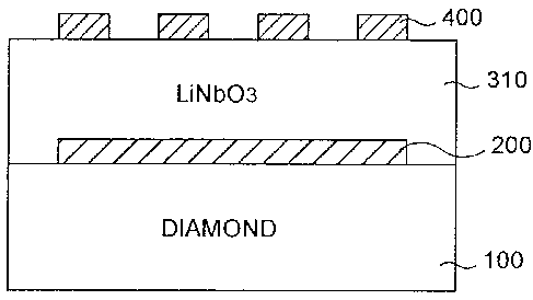
(First Embodiment)
Fig. 2 is a sectional view showing the structure
of an SAW device according to the first embodiment of
the present invention. As shown in Fig. 2, the SAW
18
2197018
SEI 96-32
device of the first embodiment comprises {a) diamond
100, (b) a short-circuit electrode 200 formed on the
diamond 100, (c) a single crystal LiNb03 layer 310
formed on the short-circuit electrode 200, and (d) an
interdigital transducer 400 formed on the LiNb03 layer
310.
In the SAW device of the first embodiment, when
the interdigital transducer 400 is used to excite an
SAW, a plurality of SAWS with different propagation
velocities V are excited (0th-order mode, 1st-order
mode, 2nd-order mode,... in ascending order of the
propagation velocities V). Therefore, the mode of an
SAW used in the SAW device can be determined by
measuring the propagation velocity V of the SAW at the
operating frequency of the device. This propagation
velocity V can be obtained from, e.g., a relation V =
f~. ( f is the center frequency; ~. is the wavelength
based on the electrode width of the interdigital
transducer 400). When the interdigital transducer 400
constituting the SAW device is a single electrode
finger structure (electrode width d) having a planar
shape as shown in Fig. 3, ~. = 4d. When the
interdigital transducer 400 is a double electrode
finger structure (electrode width d) having a planar
shape as shown in Fig. 4, ~. = 8d.
The SAW device of the first embodiment uses an SAW
19 _
za 9TO~s
SEI 96-32
in the 1st-order mode.
As the diamond 100, single crystal diamond and/or
polycrystalline diamond can be used. The method of
obtaining the diamond 100 is not particularly limited.
More specifically, single crystal diamond may be used
as the diamond. In addition, a diamond layer may be
formed on any material (substrate) by epitaxial growth
to obtain the diamond 100 as a polycrystalline diamond
layer or an epitaxial diamond layer.
The base material for forming the diamond layer is
not particularly limited and can be appropriately
selected depending on the application purpose of the
SAW device. In the first embodiment, a semiconductor
such as Si, a metal, a glass material, a ceramic, or
the like can be used as the material.
When the diamond 100 is a diamond layer, the
method of growing the diamond layer is not particularly
limited. More specifically, a known technique such as
CVD (Chemical Vapor Deposition), microwave plasma CVD,
PVD (Physical Vapor Deposition), sputtering, ion
plating, a plasma jet method, a flame method, or a hot
filament method can be used as the growth method.
The plane orientation of the diamond 100 is not
particularly limited. The diamond 100 can have a plane
orientation (111), (100), or (110), or can have two or
more of them simultaneously.
z i 9TO ~ s
SEI 96-32
When the diamond 100 is to be obtained as a layer,
the thickness of the diamond 100 is set such that khz
4 is satisfied when t~ represents the thickness of the
diamond 100, and a relation kh~ = 2~(t~/~.) holds.
If the diamond layer is thin, the SAW
characteristics vary. However, when the thickness t~
[gym) of the diamond layer is set such that khz Z 4
holds, the variation amount poses no practical problem.
More preferably, khz 2 8. In this case, the variation
amount can be further reduced.
The short-circuit electrode 200 is an electrode
having a function of setting an equipotential of an
electric field to change the SAW characteristics of the
device. The short-circuit electrode 200 is preferably
formed of a (thin) metal film (e. g., A1, Au, or A1-Cu).
Since the short-circuit electrode 200 has a function
different from that of the interdigital transducer 400,
the material of the short-circuit electrode 200 need
not be the same as that of the interdigital transducer
400.
The thickness of the short-circuit electrode 200
is not particularly limited as far as the function as a
short-circuit electrode can be obtained. However, it
is preferably about 50 to 3,000 A (more preferably,
about 100 to 500 A). When this thickness is smaller
than 50 A, it is difficult to set an equipotential. On
21
2197018
SEI 96-32
the other hand, a thickness larger than 3,000 ~ results
in a decrease in velocity of an SAW.
The short-circuit electrode 200 preferably has a
planar shape of, e.g., a "solid electrode" having the
same area as that of the interdigital transducer 400.
The material of the interdigital transducer 400 is
not particularly limited as far as it is a conductive
material. From the viewpoint of workability as an
interdigital transducer and cost, Al (aluminum) can be
particularly preferably used.
The thickness of the interdigital transducer 400
a
is preferably about 100 to 5,000 A (more preferably,
about 100 to 500 A) though it is not particularly
limited as far as the function as an interdigital
transducer can be obtained. When this thickness is
0
smaller than 100 A, the resistivity increases,
resulting in an increase in loss. On the other hand,
when the thickness of the electrode exceeds 5,000 A,
the mass addition effect which causes reflection of an
SAW due to the thickness and height of the electrode
becomes conspicuous, and desired SAW characteristics
may be impeded.
The planar shape of the interdigital transducer
400 is not particularly limited as far as the function
as an interdigital transducer can be obtained. A
so-called single electrode finger structure whose
22
2197018
SEI 96-32
schematic plan view is shown in Fig. 3 or a double
electrode finger structure whose schematic plan view is
shown in Fig. 4 can be preferably used.
The LiNb03 layer 310 is formed by bonding a cut
single crystal LiNbO, thin plate to the diamond 100
having the short-circuit electrode 200 formed on its
polished surface, and then polishing the single crystal
LiNb03 thin plate.
For the LiNb03 layer 310, a thickness ti [gym] and a
crystal orientation (e[°],~[°),~V[°]) are selected from
the following values . Note that khi ( = 2 n ( ti/ ~ ) ; ~1 =
the wavelength [gym] of an SAW) is used instead of the
thickness ti.
An arbitrarily value within the range of 0° s ~ s
360° is set. The remaining values are set for each of
integer pairs (i,k), i.e., (0,0), (0,1), (1,0), and
(1,1) on an orthogonal coordinate system (khl,e,~V).
(i) For the integer pairs (i,k), i.e., (0,0),
(0,1), (1,0), and (1,1) on the orthogonal coordinate
system (khl,e,~), values in the internal regions of four
hexahedrons each of which has, as its opposing bottom
surfaces, a planar rectangular region with its vertexes
at points Allik, Bllik, C11'k, and Dllik and a planar
rectangular region with its vertexes at points A121k~
ik ik ik
B12 , C12 , and Dlz ,
where point Aiiik - (0.45,80+1801,140+180k)
23
21970 g
SEI 96-32
point B11~'( 0 .45,100+1801,140+180k )
-
point Cliik( 0.45, 100+1801, 180+180k)
-
point Dliik( 0 . 45, 80+1801, 180+180k)
-
point Alzik( 0.7, 70+1801,120+180k)
-
point Bl~ik( 0. 7, 110+1801, 120+180k)
-
point Cl~ik(0.7, 110+1801, 180+180k)
-
point Di2ik( 0.7, 60+1801, 180+180k) .
-
(ii) For the integer pairs
(i,k), i.e., (0,0),
(0,1), (1,0), and (1,1) on the orthogonal coordinate
system (khl,e,~), values in the internal regions of four
hexahedrons each of which has, as its opposing bottom
surfaces, a planar rectangular region with its vertexes
at points Al3ik, Bl~ik, Cl9ik, and pl3ik and a planar
rectangular region with its vertexes at points Ai4ik'
ik ik ik
Bia , Cia , and D1~ ,
where point Ai3ik (0.45,80+1801,0+180k)
-
point Bl3ik ( 0.45, 90+1801, 0+180k)
-
point Ci3ik (0.45,90+1801,10+180k)
-
point Di3ik (0,45,80+1801,20+180k)
-
point A~~ik ( 0 . 7, 60+1801, 0+180k)
-
point Bl~ik ( 0 , 7, 110+1801, 0+180k)
-
point Cl,ik (0,7,90+1801,40+180k)
-
point Dl,ik ( 0. 7, 80+1801, 40+180k)
- .
In the structure of the SAW device according to
the first embodiment, the propagation velocity V is
exclusively determined by khl of the LiNb03 layer 310.
24
2197~1a
SEI 96-32
Fig. 5 is a graph showing the relationship between khl
of the LiNb03 layer 310 and the propagation velocity V
of an SAW in the 1st-order mode in the SAW device of
the first embodiment. It is confirmed from Fig. 5
that, when khl is equal to or smaller than 0.7, a
propagation velocity V equal to or higher than 8,000
m/s is ensured.
The present inventors set the thickness of the
diamond 100 at 20 Vim, and evaluated an
electromechanical coupling coefficient K' while changing
khl within the above-described limitation for khl and
simultaneously changing the values e, ~, and
Figs. 6 to 21 are graphs showing contour lines
obtained upon evaluating the electromechanical coupling
coefficient KZ [~] under conditions that khl = 0.20,
0.325, 0.45, and 0.7, ~ = 0°, 10°, 20°, and 30°,
0° s 8
180°, and 0° s ~V s 180°. Note that the values 8 and
are plotted in units of 10° in these graphs.
Regions for satisfying the electromechanical
coupling coefficient K' of 10~ or more are obtained from
Figs. 6 to 21. Taking the symmetry of the LiNb03
crystal into consideration, it is confirmed that, when
the propagation velocity V is 8,000 m/s or more, and
the electromechanical coupling coefficient K' is 10~ or
more, the value ~ is arbitrarily set within the range
of 0° S ~ s 360°, and the remaining parameters khl, 8,
2197018
SEI 96-32
and ~V are set, on the orthogonal coordinate system
{khl,g,~), in the internal regions of the four
hexahedrons represented by (i) or {ii).
(Second Embodiment)
Fig. 22 is a sectional view showing the structure
of an SAW device according to the second embodiment of
the present invention. As shown in Fig. 22, the SAW
device of the second embodiment is different from that
of the first embodiment only in that an SAW in the
2nd-order mode is used, and an LiNb03 layer 320 is
formed in place of the LiNb03 layer 310.
The LiNbO~ layer 320 is formed by bonding a cut
single crystal LiNb03 thin plate to diamond 100 having a
short-circuit electrode 200 formed on its polished
surface, and then polishing the single crystal LiNb03
thin plate.
For the LiNbO~ layer 320, a thickness tl [gym] and a
crystal orientation {e[~],~[~],~[~]) are selected from
the following values. Note that khl (= 2n(tl/~);
the wavelength [gym] of an SAW) is used instead of the
thickness tl, as in the first embodiment.
(i) 0 S ~ s 15, 45 + 60j 5 ~ S 75 + 60j (j - an
integer of 0 to 4), or 345 S ~ S 360. For integer
pairs (i,k), i.e., (0,0), (0,1), (1,0), and (1,1) on an
orthogonal coordinate system {khl,e,~), values in the
internal regions of four hexahedrons each of which has,
26
219?018
SEI 96-32
as its opposing bottom surfaces, a planar rectangular
region with its vertexes at points Azl'k, B~lik, C~lik, and
D~i'k and a planar rectangular region with its vertexes
at points A=~ik, B22ik' ~~~ik, and D~
where point A~1'''( 0.6, 60+1801, 40+180k)
-
point BZllk(0,6,110+1801,40+180k)
-
point Czls''( 0 . 6, 110+1801,120+180k
- )
point Dzlik( 0. 6, 60+1801,120+180k)
-
point A~zsk( 0. 85, 50+1801, 70+180k)
-
point B~z"'( 0 . 85,130+1801, 0+180k)
-
point Cz~l''( 0. 85, 130+1801, 180+180k)
-
point D~zi''( 0.85, 50+1801, 100+180k)
- .
(ii) 0 5 ~ 5 15, 45 + 60j 5 ~ S 75 + 60j (j - an
integer of 0 to 4), or 345 S ~ s 360. For the integer
pairs (i,k), i.e., (0,0), {0,1), (1,0), and (1,1) on
the orthogonal coordinate system (khl,e,~V), values in
the internal regions of four hexahedrons each of which
has, as its opposing bottom surfaces, the planar
rectangular region with its vertexes at the points A~~ik,
2O B~~'k, Czzsk, and Dz2lk and a planar rectangular region with
its vertexes at points A~3lk, B~3lk' '.,~3lkr and D231k'
where point A~~ik - (1.1,40+1801,60+180k)
point B~3ik - ( 1 . 1, 140+1801, 0+180k)
point C23ik - ( 1 . 1, 140+1801, 180+180k)
point D~~'k - ( 1 . 1, 40+1801, 110+180k) .
(iii) 15 + 60j s ~ s 45 + 60j (j - an integer of
- 27
Z.197~18
SEI 96-32
0 to 5). For the integer pairs (i,k), i.e., (0,0),
(0,1), (1,0), and (l, l) on the orthogonal coordinate
system (khl,e,~), values in the internal regions of four
hexahedrons each of which has, as its opposing bottom
surfaces, a planar rectangular region with its vertexes
at points Az4lk, B~'ik, C~aik~ and Dz4'k and a planar
rectangular region with its vertexes at points A~Sik,
ik ik ik
Bzs , C~5 , and Dss ,
where point Azaik - (0.6,60+1801,30+180k)
point BZ,ik - ( 0 , 6, 120+1801, 30+180k)
point Cz,ik - ( 0 . 6, 120+1801,100+180k)
point Dz~ik - ( 0 . 6, 60+1801, 100+180k)
point Azsik - ( 0 , g5, 50+1801, 30+180k)
point B~sik - ( 0 , 85, 130+1801, 30+180k)
point Czsik - ( 0 , 85,130+1801, 110+180k)
point D~sik - ( 0 , 85, 50+1801,110+180k) .
(iv) 15 + 6pj s ~ S 45 + 60j (j - an integer of 0
to 5). For the integer pairs (i,k), i.e., (0,0),
(0,1), (1,0), and (i,l) on the orthogonal coordinate
system (khl,B,~V), values in the internal regions of four
hexahedrons each of which has, as its opposing bottom
surfaces, the planar rectangular region with its
vertexes at the points Azsik, Bzsik, C~Sik, and D~Sik and a
planar rectangular region with its vertexes at points
ik ik ik ik
2 5 Az6 , Bz6 , Czb , arid D~6 ,
where point A26'k - (1,1,40+1801,30+180k)
28
2197018
SEI 96-32
pointg~bi''( 1 ,1,140+1801, 30+180k)
-
pointCz6ik ( 1 , 1, 140+1801, 120+180k)
-
pointDz6'k ( 1 . 1, 40+1801,120+180k)
- .
In the structure of the SAW device according to
the second embodiment, a propagation velocity V is
exclusively determined by khl of the LiNb03 layer 320.
Fig. 23 is a graph showing the relationship between khl
of the LiNb03 layer 320 and the propagation velocity V
of an SAW in the 2nd-order mode in the SAW device of
the second embodiment. It is confirmed from Fig. 23
that, when khl is equal to or smaller than 1.1, a
propagation velocity V equal to or higher than 8,000
m/s is ensured.
The present inventors set the thickness of the
diamond 100 at 20 Vim, and evaluated an
electromechanical coupling coefficient K' while changing
khi within the above-described limitation for khl and
simultaneously changing the values e, ~, and
Figs. 24 to 39 are graphs showing contour lines
obtained upon evaluating the electromechanical coupling
coefficient K' [~] under conditions that kh1 = 0.6,
0.85, 1.1, and 1.6, ~ = 0°, 10°, 20°, and 30°,
0° s 8 s
180°, and 0° s ~V S 180°. Note that the values 8 and
are plotted in units of 10° in these graphs.
Regions for satisfying the electromechanical
coupling coefficient K' of 10~ or more are obtained from
29
21 X7018
SEI 96-32
Figs. 24 to 39. Taking the symmetry of the LiNbO,
crystal into consideration, it is confirmed that, when
the propagation velocity V is 8,000 m/s or more, and
the electromechanical coupling coefficient K2 is 10~ or
more, the four parameters khl, g, ~, and ~V are set in
the internal regions of the four hexahedrons
represented by (i), (ii), (iii), or (iv).
(Third Embodiment)
Fig. 40 is a sectional view showing the structure
of an SAW device according to the third embodiment of
the present invention. As shown in Fig. 40, the SAW
device of the third embodiment comprises (a) diamond
100, (b) an interdigital transducer 400 formed on the
diamond 100, (c) a single crystal LiNbO, layer 330
formed on the interdigital transducer 400, and (d) a
short-circuit electrode 200 formed on the LiNb03 layer
330.
The SAW device of the third embodiment uses an SAW
in the 1st-order mode.
The LiNbO~ layer 330 is formed by bonding a cut
single crystal LiNb03 thin plate to the diamond 100
having the interdigital transducer 400 formed on its
polished surface, and then polishing the single crystal
LiNb03 thin plate. For the interdigital transducer 400,
preferably, a recessed portion is formed in the diamond
100 by reactive ion etching, the interdigital
2197018
SEI 96-32
transducer 400 is formed with A1 or the like in this
recessed portion, and the interface to the ZiNb03 layer
330 is entirely flattened.
For the LiNb03 layer 330, a thickness tl [ ~.m] and a
crystal orientation (8[°],~[°],~[°)) are selected from
the following values. Note that khl (= 2n(tl/~);
the wavelength [gym) of an SAW) is used instead of the
thickness tl, as in the first embodiment.
(i) 0 5 ~ s 15, 45 + 60j S ~ S 75 + 60j (j = an
integer of 0 to 4), or 345 5 ~ s 360. For integer
pairs (i,k), i.e., (0,0), (0,1), (1,0), and (1,1) on an
orthogonal coordinate system (khl,e,~), values in the
internal regions of four quadrangular pyramids each of
which has ,its vertex at a point P311k and, as its bottom
surface, a planar rectangular region with its vertexes
at points A~llk, B311k' C,,lik' and D3lik'
where point P3lik(0.45,90+1801,150+180k)
-
point A3lik( 0. 7, 70+1801, 130+180k)
-
point B311k( 0 . 7, 90+1801, 130+180k)
-
point C~1'k- ( 0. 7, 90+1801, 180+180k)
-
point D3l~k( 0 . 7, 70+1801, 180+180k)
- .
(ii) 15 + 6pj s ~ s 45 + 60j (j - an integer of 0
to 5). For the integer pairs (i,k), i.e., (0,0),
(0,1), (1,0), and (l, l) on the orthogonal coordinate
system (khl,e,~), values in the internal regions of four
hexahedrons each of which has, as its opposing bottom
31
2197018
SEI 96-32
surfaces, a planar rectangular region with its vertexes
at points A32ik, B3~ik' ~3~ik' and D3~ik and a planar
rectangular region with its vertexes at points A33'k~
ik ik ik
B33 ~ C33 I and D33 ,
where point A3~ik (0,45,80+1801,130+l8Ok)
-
point g321k ( 0 .45, 100+1801, 130+180k)
-
point C3zik ( 0 . 45, 100+1801, 150+180k)
-
point D3~ik ( 0. 45, 80+1801, 150+180k )
_
point A333k ( 0 . 7, 70+1801, 120+180k)
-
point B333k ( 0. 7, 110+1801, 120+180k)
_
point C333k ( 0 . 7, 110+1801, 160+180k )
_
point D333k ( 0. 7, 70+1801, 160+180k) .
-
In the structure of the SAW device according to
the third embodiment, a propagation velocity V is
exclusively determined by khl of the LiNb03 layer 330,
as in the first embodiment, as shown in Fig. 5.
Therefore, as in the first embodiment, it is confirmed
that, when khl is equal to or smaller than 1.1, a
propagation velocity V equal to or higher than 8,000
m/s is ensured.
The present inventors set the thickness of the
diamond 100 at 20 Vim, and evaluated an
electromechanical coupling coefficient R' while changing
kh1 within the above-described limitation for khl and
simultaneously changing the values e, ~, and
Figs. 41 to 56 are graphs showing contour lines
32
2197018
SEI 96-32
obtained upon evaluating the electromechanical coupling
coefficient K' [~] under conditions that khl = 0.2,
0.325, 0.45, and 0.7, ~ = 0°, 10°, 20°, and 30°,
0° s 8
180°, and 0° s ~ s 180°. Note that the values a and
~ are plotted in units of 10° in these graphs.
Regions for satisfying the electromechanical
coupling coefficient K~ of 10~ or more are obtained from
Figs. 41 to 56. Taking the symmetry of the LiNb03
crystal into consideration, it is confirmed that, when
the propagation velocity V is 8,000 m/s or more, and
the electromechanical coupling coefficient K~ is 10~ or
more, the four parameters khl, e, ~, and ~ are set in
the internal regions of the four quadrangular pyramids
represented by (i) or the four hexahedrons represented
by (ii).
(Fourth Embodiment)
Fig. 57 is a sectional view showing the structure
of an SAW device according to the fourth embodiment of
the present invention. As shown in Fig. 57, the SAW
device of the fourth embodiment is different from that
of the third embodiment only in that an SAW in the
2nd-order mode is used, and an LiNb03 layer 340 is
formed in place of the LiNb03 layer 330.
The LiNb03 layer 340 is formed by bonding a cut
single crystal LiNb03 thin plate to diamond 100 having a
short-circuit electrode 200 formed on its polished
33
z ~ q7o n s
SEI 96-32
surface, and then polishing the single crystal LiNb03
thin plate. As in the third embodiment, for an
interdigital transducer 400, preferably, a recessed
portion is formed in the diamond 100 by reactive ion
etching, the interdigital transducer 400 is formed with
A1 or the like in this recessed portion, and the
interface to the LiNbO, layer 340 is entirely flattened.
For the LiNb03 layer 340, a thickness tl [ ~.m] and a
crystal orientation (8[°],~[°],fir[°)) are selected from
the following values. Note that khl (= 2n(tl/~.);
the wavelength [I~m] of an SAW) is used instead of the
thickness tl, as in the first embodiment.
(i) 0 s ~ s 15, 45 + 60j s ~ s 75 + 60j (j - an
integer of 0 to 4), or 345 s ~ s 360. For integer
pairs (i,k), i.e., (0,0), (0,1), (1,0), and (1,1) on an
orthogonal coordinate system (khl,0,~), values in the
internal regions of four hexahedrons each of which has,
as its opposing bottom surfaces, a planar rectangular
region with its vertexes at points Aal"', Balik, ~allk, and
Dal' and a planar rectangular region with its vertexes
at points Aa2tk, Ba=ix' Ca3ik~ and Da~lk,
where point Aal'k(0.6,70+1801,40+180k)
-
point B4l~k( 0. 6, 100+1801, 40+180k
- )
point C,11''( 0 . 6, 100+1801, 110+180k)
-
point Dal'k( 0 . 6, 70+1801, 110+180k)
-
point Aazik( 0 . 85, 70+1801, 60+180k)
-
- 34
Z197~~8
SEI 96-32
pointB4~Sk( 0 . 85,120+1801, 0+180k)
-
pointCazlk( 0 , 85, 120+1801,180+180k)
-
pointD,zlk( 0 . 85, 70+1801,100+180k)
- .
(ii) 0 s ~ s 15, 45 + 60j s ~ s 75 + 60j (j - an
integer of 0 to 4), or 345 s ~ s 360. For the integer
pairs (i,k), i.e., (0,0), (0,1), (1,0), and (1,1) on
the orthogonal coordinate system (khl,8,~), values in
the internal regions of four hexahedrons each of which
has, as its opposing bottom surfaces, the planar
rectangular region with its vertexes at the points A,zlk,
B~zik, Cask, and D"ik and a planar rectangular region with
its vertexes at points A431k, B43ik' C43ik~ and D,~ik,
where point A,3lk - ( 1 . 1, 90+1801, 0+180k)
point Ba3lk - ( 1 . 1,130+1801, 0+180k)
point C,3lk - ( 1. 1, 130+1801, 180+180k)
point D~3sk - ( 1. 1, 90+1801,180+180k) .
(iii) 15 + 6pj s cø s 45 + 60j (j = an integer of
0 to 5). For the integer pairs (i,k), i.e., (0,0),
(0,1), (1,0), and (1,1) on the orthogonal coordinate
system (khl,B,V~), values in the internal regions of four
hexahedrons each of which has, as its opposing bottom
surfaces, a planar rectangular region with its vertexes
at points Aaa'k, B4,lk, Caaik, and Daaik and a planar
rectangular region with its vertexes at points A451k'
ik ik lk
2 5 B45 . Ca5 r and D
where point A,4ik - (0.6,70+1801,20+180k)
2191018
SEI 96-32
point B"Sk - (0.6,110+1801,20+180k)
point C"Sk - (0.6,100+1801,90+180k)
point D"Sk - (0.6,70+1801,90+180k)
point A,Sik - ( 0 . 85, 60+1801, 10+180k)
point g,sik - ( 0. 85, 120+1801, 10+180k)
point C451k - ( 0 . 85, 120+1801, 90+180k)
point D,SIk - ( 0 . 85, 60+1801, 90+180k) .
(iv) 15 + 60j s ~ 5 45 + 60j (j - an integer of 0
to 5). For the integer pairs (i,k), i.e., (0,0),
(0,1), (1,0), and (1,1) on the orthogonal coordinate
system (khl,B,~V), values in the internal regions of four
hexahedrons each of which has, as its opposing bottom
surfaces, the planar rectangular region with its
vertexes at the points A,Sik, Besik' Casik' and D,5lk and a
planar rectangular region with its vertexes at points
ik Sk Sk ik
A,6 , 8,6 , C,6 , arid D,6 ,
where point A,6lk - (1.1,80+1801,10+180k)
point g,6lk - ( 1 . 1, 120+1801, 10+180k)
point C~6lk - ( 1 , 1, 130+1801, 80+180k)
point D,blk - ( 1 , 1, 50+1801, 80+180k) .
In the structure of the SAW device according to
the fourth embodiment, a propagation velocity V is
exclusively determined by khi of the LiNbO~ layer 320.
Fig. 23 is a graph showing the relationship between khl
of the LiNbO~ layer 340 and the propagation velocity V
of an SAW in the 1st-order mode in the SAW device of
~6
2197018
SEI 96-32
the fourth embodiment. It is confirmed from Fig. 23
that, when khl is equal to or smaller than 1.1, a
propagation velocity V equal to or higher than 8,000
m/s is ensured.
The present inventors set the thickness of the
diamond 100 at 20 wm, and evaluated an
electromechanical coupling coefficient K~ while changing
khl within the above-described limitation for khl and
simultaneously changing the values e, ~, and
Figs. 58 to 73 are graphs showing contour lines
obtained upon evaluating the electromechanical coupling
coefficient K' [$] under conditions that khl = 0.6,
0.85, 1.1, and 1.6, ~ = 0°, 10°, 20°, and 30°,
0° s 8 s
180°, and 0° s ~V s 180°. Note that the values ~ and
are plotted in units of 10° in these graphs.
Regions for satisfying the electromechanical
coupling coefficient K' of 10~ or more are obtained from
Figs. 58 to 73. Taking the symmetry of the LiNb03
crystal into consideration, it is confirmed that, when
the propagation velocity V is 8,000 m/s or more, and
the electromechanical coupling coefficient K' is 10~ or
more, the four parameters khl, 8, ~, and ~V are set in
the internal regions of the four hexahedrons
represented by (i), (ii), (iii), or (iv).
(Fifth Embodiment)
Fig. 74 is a sectional view showing the structure
37
2~97o~a
SEI 96-32
of an SAW device according to the fifth embodiment of
the present invention. As shown in Fig. 74, the SAW
device of the fifth embodiment comprises (a) diamond
100, (b) a single crystal LiNb03 layer 350 formed on an
interdigital transducer 400, and (c) the interdigital
transducer 400 formed on the diamond 100.
The SAW device of the fifth embodiment uses an SAW
in the 1st-order mode.
The LiNbO~ layer 350 is formed by bonding a cut
single crystal LiNbO, thin plate to the diamond 100
having the interdigital transducer 400 formed on its
polished surface, and then polishing the single crystal
LiNb03 thin plate.
For the LiNb03 layer 350, a thickness tl [ ~.m] and a
crystal orientation (8['],~['],~V[~]) are selected from
the following values. Note that khl (= 2n(tl/~);
the wavelength [~.m] of an SAW) is used instead of the
thickness tl, as in the first embodiment.
(i) For integer pairs (i,k), i.e., (0,0), (0,1),
(1,0), and (1,1) on an orthogonal coordinate system
(khl,e,~), values in the internal regions of four
quadrangular pyramids each of which has its vertex at a
point Pslik and, as its bottom surface, a planar
rectangular region with its vertexes at points Asl~k,
Sk Sk Sk
2 5 B51 , C51 , and D51 ,
where point PSlik - ( 0. 6, 90+1801, 0+180k)
38
217018
SEI 96-32
point ASlik( 0 . 7, 80+1801, 0+180k
- )
point Bslik( 0 . 7,119+180i, 0+180k
- )
point Cslik( 0 . 7,110+180i, 10+180k
- )
point Dsiik( 0 . 7, 80+1801, 10+180k)
- .
(ii) For the integer pairs (i,k), i.e., (0,0),
(0,1), (1,0), and (1,1) on the orthogonal coordinate
system (khi,B,V~), values in the internal regions of four
quadrangular pyramids each of which has its vertex at a
point ps~ik and, as its bottom surface, a planar
rectangular region with its vertexes at points As~ikr
ik ik Sk
BSZ , C5Z , and DSZ ,
where point ps~ik - (0.6,100+1801,0+180k)
point AS=ik - ( 0. 7, 90+1801, 170+180k)
point Bs~ik - ( 0. 7,100+1801,170+180k)
point C521k - ( 0 . 7, 110+1801, 180+180k)
point Ds~ik - ( 0 . 7, 80+1801, 180+180k ) .
In the structure of the SAW device according to
the fifth embodiment, a propagation velocity V is
exclusively determined by khl of the LiNb03 layer 350,
as in the first embodiment, as shown in Fig. 5.
Therefore, as in the first embodiment, it is confirmed
that, when khl is equal to or smaller than 1.1, a
propagation velocity V equal to or higher than 8,000
m/s is ensured.
The present inventors set the thickness of the
diamond 100 at 20 I~m, and evaluated an
39
219708
SEI 96-32
electromechanical coupling coefficient K' while changing
khl within the above-described limitation for khl and
simultaneously changing the values 8, ~, and ~V.
Figs. 75 to 90 are graphs showing contour lines
obtained upon evaluating the electromechanical coupling
coefficient K~ [~] under conditions that khl = 0.2,
0.325, 0.45, and 0.7, ~ = 0°, 10°, 20°, and 30°,
0° s 8
s 180°, and 0° s ~ s 180°. Note that the values a and
are plotted in units of 10° in these graphs.
Regions for satisfying the electromechanical
coupling coefficient K' of 10~ or more are obtained from
Figs. 75 to 90. Taking the symmetry of the LiNbO~
crystal into consideration, it is confirmed that, when
the propagation velocity V is 8,000 m/s or more, and
the electromechanical coupling coefficient K' is 10$ or
more, the four parameters khl, 8, ~, and ~ are set in
the internal regions of the four quadrangular pyramids
represented by (i), (ii), (iii), or (iv).
(Sixth Embodiment)
Fig. 91 is a sectional view showing the structure
of an SAW device according to the sixth embodiment of
the present invention. As shown in Fig. 91, the SAW
device of the sixth embodiment is different from that
of the fifth embodiment only in that an SAW in the
2nd-order mode is used, and an LiNbO~ layer 360 is
formed in place of the LiNb03 layer 350.
2197018
SEI 96-32
The LiNb03 layer 360 is formed by bonding a cut
single crystal LiNb03 thin plate to diamond 100 having a
short-circuit electrode 200 formed on its polished
surface, and then polishing the single crystal LiNb03
thin plate, as in the fifth embodiment.
For the LiNb03 layer 360, a thickness ti [gym] and a
crystal orientation (e[~],~[~],~[~]) are selected from
the following values . Note that khi (= 2n ( tl/~. ) ;
the wavelength [gym] of-an SAW) is used instead of the
thickness ti, as in the first embodiment.
(i) 0 S ~ s 15, 45 + 60j s ~ s 75 + 60j (j - an
integer of 0 to 4), or 345 S ~ s 360. For integer
pairs (i,k), i.e., (0,0), (0,1), (1,0), and (1,1) on an
orthogonal coordinate system (khl,e,~), values in the
internal regions of four hexahedrons each of which has,
_as its opposing bottom surfaces, a planar rectangular
region with its vertexes at points Asiik, B611k, C611k, and
Dbiik and a planar rectangular region with its vertexes
at points A6~ik, B6~ik, C621k' and D6~ik,
where point Aslik(0.85,140+1801,40+180k)
-
point B611k( 0. 85, 160+1801, 40+180k)
-
point Cblik( 0 . 85, 160+1801, 60+180k)
-
point D611k( 0 . 85, 140+1801, 60+180k
- )
point A621k( 1, 1, 120+1801, 30+180k)
-
point gb=lk(1,1,170+1801,30+180k)
-
point Ca~ik( 1 , 1 , 170+1801, 70+180k)
-
41
2~ 9018
SEI 96-32
point D6~ik - ( 1.1, 120+1801, 70+180k) .
(ii) 0 s ~ s 15, 45 + 60j s ~ s 75 + 60j (j - an
integer of 0 to 4), or 345 s ~ s 360. For the integer
pairs (i,k), i.e., (0,0), (0,1), (1,0), and (1,1) on
the orthogonal coordinate system (khl,e,~), values in
the internal regions of four hexahedrons each of which
has, as its opposing bottom surfaces, a planar
rectangular region with its vertexes at points Ab3ik,
B631k~ ~b3lk~ and Db3i'' and a planar rectangular region with
its vertexes at points As,i'', Bs~lk, C6~''',
and D64
where point Ab3i'' ( 0 . 85, 130+1801,130+180k)
-
point Bb31'' { 0 . 85,160+1801, 130+180k)
-
point Cb3s'' { 0 .85,160+1801,150+180k
- )
point Db31'' ( 0.85, 130+1801, 150+180k)
-
point Ab,i'' ( 1 , 1, 100+1801, 140+180k)
-
point Bb,;'' ( 1 .1, 140+1801, 100+180k)
-
point Cs,ik ( 1.1,160+1801, 160+180k)
-
point Db'i'' ( 1 :1, 130+1801, 160+180k)
- .
(iii) 0 s ~ s 15, 45 + 60j s ~ s 75 + 60j (j - an
integer of 0 to 4), or 345 s ~ s 360. For the integer
pairs (i,k), i.e., (0,0), (0,1), (1,0), and (1,1) on
the orthogonal coordinate system (kh~,e,~V), values in
the internal regions of four quadrangular pyramids each
of which has its vertex at a point PbSik and, as its
bottom surface, a planar rectangular region with its
vertexes at points Abslk, B651k ~ ~651k ~ and D6~
42
2197018
SEI 96-32
where point Pssik - (0.85,30+1801,90+180k)
point A651k - ( 1 .1, 20+1801, 70+180k)
point B651'' - ( 1.1, 40+1801, 70+180k)
point C651k - ( 1.1, 40+1801,110+180k )
point D651k - ( 1.1, 20+1801, 110+180k) .
(iv) 15 + 60j s ~ s 45 + 60j (j = an integer of 0
to 5). For the integer pairs (i,k), i.e., (0,0),
(0,1), (1,0), and (1,1) on the orthogonal coordinate
system (khl,e,~V), values in the internal regions of four
hexahedrons each of which has, as its opposing bottom
surfaces, a planar rectangular region with its vertexes
at points A661k, B661k, Cbsik, and D661k and a planar
rectangular region with its vertexes at points pb~ik~
ik ik ik
B6~ , C6~ , and D6~ ,
where point A661k( 0.6, 20+1801,150+i80k)
-
point B661k( 0 . 6, 40+1801, 150+180k)
-
point Cbsik( 0. 6, 40+1801, 170+180k)
-
point D661k( 0.6, 20+1801,170+180k)
-
point As~ik(0.85,50+1801,130+180k)
-
point gs~ik( 0 . 85, 70+1801, 140+180k)
-
point C6~ik( 0 . 85 , 50+1801, 160+180k
- j
point D6~sk(0.85,20+1801,160+180kj.
-
(v) 15 + 60j S ~ s 45 + 60j (j - an integer of 0
to 5). For the integer pairs (i,k), i.e., (0,0),
(0,1), (1,0), and (1,1) on the orthogonal coordinate
system (khl,e,V~), values in the internal regions of four
43
21970!8
SEI 96-32
hexahedrons each of which has, as its opposing bottom
surfaces, the planar rectangular region with its
vertexes at the points A67ik, B6'ik/ C6'ik' and D6~ik and a
planar rectangular region with its vertexes at points
Aseik, Bs8lk, C681k, and DbBlk,
where point Aseik - (1.1,40+1801,120+180k)
point B6eik - ( 1.1, 90+1801,120+180k)
point C681k - ( 1.1, 90+1801, 160+180k)
point D681k - ( 1 . 1, 40+1801, 160+l8pk) .
(vi) 15 + 60j s ~ s 45 + 60j (j = an integer of 0
to 5). For the integer pairs (i,k), i.e., (0,0),
(0,1), (1,0), and (1,1) on the orthogonal coordinate
system (khl,e,~), values in the internal regions of four
hexahedrons each of which has, as its opposing bottom
surfaces, a planar rectangular region with its vertexes
at points A691k' B691k, C691k~ and D691k and a planar
rectangular region with its vertexes at points A6Aik,
ik ik ik
B6A , C6~ , and D6A ,
where point Ab9lk(0,6,140+1801,150+180k)
-
point g691k( 0 . 6, 160+1801, 150+180k)
-
point C691k( 0 . 6, 160+1801, 160+180k)
-
point D691k( 0 .6, 140+1801, 160+180k)
-
point A6Aik( 0 . 85, 100+1801, 140+180k)
-
point B6A'k( 0.85, 130+1801, 130+180k)
-
point C6A1"( 0 . 85, 160+1801, 160+180k)
-
point DsA'k( 0 .85, 130+1801, 160+180k)
- .
44
2197018
SEI 96-32
(vii) 15 + 60j s ~ s 45 + 60j (j = an integer of
0 to 5). For the integer pairs (i,k), i.e., (0,0),
(0,1), (1,0), and (1,1) on the orthogonal coordinate
system (khl,e,~V), values in the internal regions of four
hexahedrons each of which has, as its opposing bottom
surfaces, the planar rectangular region with its
vertexes at the points A6yk, B6Aik, C6A~, and D6~ik and a
planar rectangular region with its vertexes at points
ik B ik ~ ik and D ik
6H ~ 6H ~ 6H ~ 6H
where point A6Hik - (1.1,100+1801,120+180k)
point Bbeik - ( 1.1, 150+1801, 120+180k)
point Cbeik - ( 1 .1, 150+1801, 160+180k)
point D6Hik - ( 1 . l, 100+1801, 160+180k) .
(viii) 15 + 60j s ~ s 45 + 60j (j = an integer of
0 to 5). For the integer pairs (i,k), i.e., (0,0),
(0,1), (1,0), and (1,1) on the orthogonal coordinate
system ( khl, 8, ~V ) , values in the internal regions of four
hexahedrons each of which has, as its opposing bottom
surfaces, a planar rectangular region with its vertexes
at points Abcik, BbCik' C6Cik, and Db~ik and a planar
rectangular region with its vertexes at points pl6Dik,
B.6D1K, C6Dik, and D6Dik ,
where point As~ik(0.85,150+1801,50+180k)
-
point B6~ik( 0 . 85 , 160+1801,
- 50+180k )
point C6~ik( 0 . 85, 160+1801,
- 60+180k)
point D6~'k( 0 . 85, 150+1801,
- 60+180k)
2I91018
SEI 96-32
point A6pik - ( 1 . 1, 130+1801, 40+180k)
point g6oik - ( 1. 1, 160+1801, 40+180k)
point Cspik - ( 1 . 1,160+1801, 90+180k)
point Dsoik - ( 1 .1, 130+1801, 90+180k) .
(ix) 15 + 60j s ~ s 45 + 60j (j = an integer of 0
to 5). For the integer pairs (i,k), i.e., (0,0),
(0,1), (1,0), and (1,1) on the orthogonal coordinate
system (kh,,~,~), values in the internal regions of four
quadrangular pyramids each of which has its vertex at a
point p6Lik and, as its bottom surface, a planar
rectangular region with its vertexes at points A6~Sk~
ik ik ik
B6~ , C6E , and
where point p6~ik(p.85,30+1801,70+180k)
-
point As~ik( 1 . 1, 20+1801, 50+180k)
-
point B6~ik( 1 .1, 40+1801, 50+180k)
-
point C6Lik( 1 . 1, 40+1801, 90+180k)
-
point D6Eik( 1 . 1, 20+1801, 90+180k)
- .
In the structure of the SAW device according to
the sixth embodiment, a propagation velocity V is
exclusively determined by khi of the LiNb03 layer 360,
as in the second embodiment, as shown in Fig. 23.
Therefore, it is confirmed that, when khl is equal to or
smaller than l.l, a propagation velocity V equal to or
higher than 8,000 m/s is ensured.
The present inventors set the thickness of the
diamond 100 at 20 I~m, and evaluated an
46
Zl 970 I 8
SEI 96-32
electromechanical coupling coefficient K' while changing
khl within the above-described limitation for khl and
simultaneously changing the values 8, ~, and
Figs. 92 to 107 are graphs showing contour lines
obtained upon evaluating the electromechanical coupling
coefficient K' [$] under conditions that khl = 0.6,
0.85, 1.1, and 1.6, ~ = 0°, 10°, 20°, and 30°,
0° s 8 s
180°, and 0° s ~V s i80°. Note that the values a and
are plotted in units of 10° in these graphs.
Regions for satisfying the electromechanical
coupling coefficient K~ of 10$ or more are obtained from
Figs. 92 to 107. Taking the symmetry of the LiNb03
crystal into consideration, it is confirmed that, when
the propagation velocity V is 8,000 m/s or more, and
the electromechanical coupling coefficient K~ is 10~ or
more, the four_parameters khl, e, ~, and ~ are set in
the internal regions of the four hexahedrons
represented by (i), (ii), (iv), (v), (vi), (vii), or
(viii), or the four quadrangular pyramids represented
by (iii) or (ix).
(Seventh Embodiment)
Fig. 108 is a sectional view showing the structure
of an SAW device according to the seventh embodiment of
the present invention. As shown in Fig. 108, the SAW
device of the seventh embodiment comprises (a) diamond
100, (b) an interdigital transducer 400 formed on the
47
2191018
SEI 96-32
diamond 100, and (c) a single crystal LiNb03 layer 370
formed on the interdigital transducer 400.
The SAW device of the seventh embodiment uses an
SAW in the 2nd-order mode.
The LiNb03 layer 370 is formed by bonding a cut
single crystal LiNb03 thin plate to the diamond 100
having the interdigital transducer 400 formed on its
polished surface, and then polishing the single crystal
LiNb03 thin plate. As in the third embodiment, for the
interdigital transducer 400, preferably, a recessed
portion is formed in the diamond 100 by reactive ion
etching, the interdigital transducer 400 is formed with
A1 or the like in this recessed portion, and the
interface to the LiNbO~ layer 370 is entirely flattened.
For the LiNb03 layer 370, a thickness tl [ ~.m] and a
crystal orientation (8[°],~[°],~[°]) are selected from
the following values . Note that khl ( = 2n ( ti/~. ) ;
the wavelength [gym] of an SAW) is used instead of the
thickness tl, as in the first embodiment.
15 + 60j 5 ~ s 45 + 60j (j - an integer of 0 to
5). For integer pairs (i,k), i.e., {0,0), (0,1),
(1,0), and (l, l) on an orthogonal coordinate system
{khl,e,~), values in the internal regions of four
hexahedrons each of which has, as its opposing bottom
surfaces, a planar rectangular region with its vertexes
at points A~1'k, g~11'', C~1"', and D~i'k and a planar
48
219~'0~8
SEI 96-32
rectangular region with its vertexes at points A,~Sk'
ik ik Sk
B,z , C,~ , and D,~ ,
where point A,lik - (0.85,50+1801,160+180k)
point B711k- ( 0 .85,100+1801,160+180k)
point C,lik( 0 , g5, 90+1801, 170+180k )
-
point D,lik( 0 , g5, 50+1801, 170+180k )
-
point A,~ik( 1. l, 40+1801,150+180k)
-
point B,zik( 1 . 1, 140+1801,150+180k )
-
point C,Zik( 1 . 1, 140+1801, 180+180k)
-
point D,zik( 1.1, 40+1801, 180+180k) .
-
In the structure of the SAW device according to
the seventh embodiment, a propagation velocity V is
exclusively determined by kh1 of the LiNb03 layer 370,
as in the second embodiment, as shown in Fig. 23.
Therefore, it is confirmed that, when khl is equal to or
smaller than 1.1, a propagation velocity V equal to or
higher than 8,000 m/s is ensured.
The present inventors set the thickness of the
diamond 100 at 20 ~.m, and evaluated an
electromechanical coupling coefficient K' while changing
khl within the above-described limitation for khl and
simultaneously changing the values ~, ~, and
Figs. 109 to 124 are graphs showing contour lines
obtained upon evaluating the electromechanical coupling
coefficient K2 (~) under conditions that khl = 0.6,
0.85, 1.1, and 1.6, ~ = 0°, 10°, 20°, and 30°,
0° s 8 s
49
2197018
SEI 96-32
180°, and 0° s ~ s 180°. Note that the values 8 and
are plotted in units of 10° in these graphs.
Regions for satisfying the electromechanical
coupling coefficient K' of 10~ or more are obtained from
Figs. 109 to 124. Taking the symmetry of the LiNb03
crystal into consideration, it is confirmed that, when
the propagation velocity V is 8,000 m/s or more, and
the electromechanical coupling coefficient K' is 10~ or
more, the four parameters khl, e, ~, and ~ are set in
the internal regions of the above four hexahedrons.
The present inventors evaluated an
electromechanical coupling coefficient K~ of an SAW
device having the same structure as in the seventh
embodiment and using the 1st-order mode while changing
khl and simultaneously changing the values ~, ~, and
Figs. 125 to 140 are graphs showing contour lines
obtained upon evaluating the electromechanical coupling
coefficient K2 [~] under conditions that khl = 0.2,
0.325, 0.6, and 0.7, ~ = 0°, 10°, 20°, and 30°,
0° s 8
s 180°, and 0° s ~ s 180°. Note that the values a and
are plotted in units of 10° in these graphs.
It is confirmed from Figs. 125 to 140 that no
region for satisfying the electromechanical coefficient
K~ Z 10~ is present.
From the invention thus described, it will be
obvious that the invention may be varied in many ways.
CA 02197018 2004-06-22
Such variations are not to be regarded as a departure
from the spirit and scope of the invention, and all
such modifications as would be obvious to one skilled
in the art are intended for inclusion within the scope
of the following claims.
S1