Note: Descriptions are shown in the official language in which they were submitted.
~~ WO 96/05s36 '2 1 3 7 3 2 8 P~,ll.J.,, " 1~
OPTOELECTRONIC COUPLER
Ra. 1~ ~ ld of th. Inventi-m
Field of the TnventiQn --
This invention relates to an optoelectronic coupler. Two
applications for the coupler are as an optical modulator or as an optical
detector.
Recent advances in technology have resulted in an emphasis on the
photonics field - the field which concerns the generation, lll~i~ul.lLion,
mo~ tion and detection of light and optical waves, where light and
optical are taken to refer to the ultraviolet, visible, near-infrared and mid-
infrared regions (up to w~-~lell~;LLs of approximately 15 ~m) of the
ele~Ll..",~,"~tic spectrum. There has also been a co~ ol1ding increase in
15 interest in photonic devices.
Specifically, optical morl~ tor.c which modulate the properties of
optical waves incident upon them and detectors which sense the strength
of incident waves are two fim~l~m~nt~l building blocks for almost all
photonics systems. For example, optical fibers are becoming more
20 prevalent with each passing day, and, in such a system, inform~tion is
~UIIII~IIIIIi~ Alr'ri by encoding the infnrm~tinn on a light beam, Ll~ ll;ll;llgthe beam to the receiver, and decoding the received beam. The encoding
can be achieved by using a constant light source mndnl~n-d by an optical
mo~ tor, and a detector is required to decode the received beam. As
2~ another example, as ~Ulll~JUL..S become more powerful, they are becoming
"" " " " . " ;. ~ n c-limited rather than processor-limited. That is, the
bottleneck on computer speed tends to lie more and more in the time
required to cnmmllni~t~ between various parts of the computer rather
than in the time required to perform the computations. One potential
30 solution is to use optical rather than electronic ill~ olll.e.~ since
photonics technology offers a potentially large speed advantage. In such an
_ _ , .. .. .. ...... . . . ..
2~9~32~
PCTIUS95110313 --
WO 96/05536
approach, optical mOf~ tf~rS and detectors may be used to encode and
decode bits in much the same manner as in fiber systems. As a final
example, the advent of mass storage devices and high bandwidth
c~lmmnni~tif)nC channels in allowing our society to move towards picture-
5 based c~mmllni~tifmcJ the explosion in the number of fax machines andthe amount of television p~ lhlg being prime examples, and the
display and capture of these images requires both modnl~tclr~ and
detectors. In a fax machine, detectors may be used to capture the image
on the transmit side while mt~ tr)rc may be used to recreate the image, a
10 la laster printers, on the receive side. Detectors and mo~llll~t~rs may play
similar roles in the tranC~nic~;on of video. As a direct result of these
tP~hnol-)gi~l advances, there is an ever increasing demand for these devices
and improvements in these devices.
However, devices such as detectors and modlll~torc which bridge the
15 gap between electrons and photons must rely on fimd~mPnrll physical
phPnnmPn~ In the context of this invention, the phPnllmPn l relied upon
are primarily the coupling of optical waves to one another, the application
or sensing of electronic effects through electrodes, and the interaction of
photons aud electrons in special material systems, such as cPmin~nrlllrt~rc
20 or electro-optic materials. Therefore, advances in these devices depend in
large part on either designs which enhance the basis physical effects or
practical advances, such as i~ s in device cost, reliability,
f~hrif~rinn, ease of operation, etc.
25 Description of the Related Art
Since the invention lies at the intPrCPCtiCm of several fields, the
related art may also be divided into distinct areas. For convenience,
complete reference citations are collected in the last section of the
description of the preferred embodiment.
WO 96/OS536 2 1 9 7 3 2 8 PCT/US9S/10313
One area of related art concerns the design of gratings to couple
between optical waves. For example, Maystre et al.,"On a General Theory
of Anomalies and Energy Absorption by Diffraction Gratings and Their
Relation with Surface Waves," Optica Acta" 25, 905-915 (1978);
5 M:~grnl1c~r n, R., and Wang, S.S., "Optical Guided-mode Resonance Filter,"
U.S. Patent No. 5~216,680 (June 1, 1993); Delort, T., and Maystre, D.,
"Finite Element Method for Gratings," J. C)pt. Soc. Am. A., 10, 2592 (1993);
and Vincent, P., "Integral Equation Computation of Bump Grating
F.ffi~i~nfiPc in TE Pol~ri7~titm, "J. Opt. Soc. Am. A., 10, 444 (1993), the
10 teachings of which are incorporated herein by reference, describe
approaches by which the detailed optical properties of the structures
described herein may be r~lr~ ter~ Thee descriptions are complete
ele~LIu~ tic treatments and include the excitation of surface plasmons,
total-internal-reflection (TIR) guided waves, and surface ~ vr~cs~~rl~ waves.
15 For ~ul~ r, the term local wave will be used to refer to these three
types of waves. Campbell, P., "F.nh~nl~f-m~-nt of Light Absorption from
R ln-lomi ~ing and Geometric Textures," J. Opt. Soc. Am. B., 10, 2410 (1993)
theoretically describes the ~nh~n~mPm of light absorption in textured
surfaces using a greom. tri~l approach. Sambles, J.R. et al., "Optical
20 F.Yrit~tit~n of Surface Plasmons: An Introduction, "Cu"~ iu~ ly Physics,
32, 173-183 (1991) ~iescribes the general theory of optical excitation of
surface plasmons, inclu&g the use of periodic structures, and Bryan-
Brown, G.P. et al., "Coupled Surface Plasmons on Silver Coated Gratings,"
Optics G~ ;Q~S~ 82, 1 (1991) describes the coupling of surface
25 plasmons to each other. While the teachings of these references may be
used to design certain aspects of the current invention, the references
themselves are primarily directed towards the purely optical coupling of
~ waves via static structures. The issue of dynamic operation of the devices
is ~ r-- l-.- ily addressed, as are any electrical aspects.
W096/0~36 2 ~ ~ 73?~; PCIIUS95110313--
There are devices which rely on both the coupling of optical waves
and some sort of electrical ~ln~titln llity. One application area is that of
waveguide mn~ t-~rc Simon, H.J. and Lee, C.H., "Electro-Optic Total
Internal Reflection Mo~ tion," Optics Letters, 13, 440 (1988) and
5 Caldwell, M.E. and Yeatman, E.M., "Recent Advances in Surface Plasmon
Spatial Light Mod~ t-)r~," SPIE P~U~1L~ . Optics for Computers--
Al.~,.L~.L~ and Tec~mologies, 1505, 50 (1991) describe dynamic coupling
between a wave external to the device and a TIR guided wave or a surface
plasmon, ~ Li~ly. However, the coupling is achieved by prism-
10 coupling or frustrated total internal reflection coupling, which has severalpractical disadvantages compared to the approach of grating coupling used
n the current invention. In the area of grating mndlll~tors, Evans, A.E.,
and Hall, D.G., "Propagation Loss Me~U1~ ,L~ in Silicon-on-Insulator
Optical Waveguides Formed by Bond-and-Etchback Process," Applied
Physics Letters, 59, 1667-1669 (1991) and Collins, R T., et al., "Optical
Mo~lnl~t~r~" U.S. Patent No. 4,915,482 (April 10, 1990) both teach the use
of a grating to couple between optical waves and, furthermore, the
coupling efficiency is m~ ted by varying a voltage impressed across part
of the structure. However, the entire grating is held at one potential and
20 the voltage difference is impressed between the grating and another part of
the structure, typically the bulk of a substrate. This is nn~c~rt~hl~
because forming electrodes in this fashion and then hut~ g a voltage
across the bulk of the device results in a slow operating speed for the
device. A similar situation exists with respect to M~gnllccr~n, R., and
25 Wang, S.S., "Optical Guided-mode Resonance Filter," U.S. Patent No.
5,216,680 aune 1, 1993); Wang, S.S., and M~gmlcs~n, R., "Theory and
Applications of Guided Mode Resonance Filters," Applied Optics, 32, 2606
(1993); and F~os~nhl ~tt, D., "Distributed Resonant Cavity Light Beam
Mr~ tor," U.S. Patent No. 5,157,537 (October 20, 1992). They teach the
30 use of a grating as a coupling device and suggest methods for electrically
~ 21973~8 '
WO 96/05536 PcTlus9sllo3l3
varying the optical properties of the grating. However, the electrodes are
not adapted for fast operation of the device, as discussed previously.
Furthermore, an additional structure is often required LO achieve the
electrical function, resulting in a more complicated device. In the area of
5 detectors, Brueck, S.R.J., et aL, "Enhanced Quantum Efficiency Internal
Photo~mic~ion Detectors by Grating Coupling to Surface Plasma Waves,"
Applied Physics Letters, 46, 915 (1985) has hlv~ dLed the use of gratings to
couple the incident light to the detector active region, thus increasing the
quantum efficiency of the detector. However, as in the devices discussed ::
above, the electrode structure used to sense the generated pho~o~ull~llL is
not adapted to permit high speed operation of the device.
Another area of related art is the general field of optical modulators.
As a l~lc~nLdLiv~ sample of the general literature, Lentine, A.L., et al.,
"Symmetric Self-Electro-optic Effect Device: Optical Set-Reset Latch,
Differential Logic Gate, and Differential Mnd~ tnr Detector," IEEE ~
Quantum Electronics, 25, 1928 (1989); Pezeshki, B., et al., '~Optimi~ ~tinn of
Mn~llll~tinn Ratio and Insertion Loss in Reflective Ele~kodbsol~ion
Modulators,~ Applied Physics Letters, 57, 1491 (1990); Treyz, G.V., et al.,
"GaAs Multiple Quantum Well ~aveguide Mo~ trrc on Silicon
Substrates," Applied Physics Letters, 57, 1078 (1990); and Xiao, X., et al.,
"Fabry-Perot Optical Intensity Modlll~tnr at 1.3 ~m in Silicon," IEEE
Photonics Technology Letters, 3, 230 (1991) all teach types of optical
mnd~ tnr.c which are not directly related to the current invention. In
particular, they differ from the current invention in at least one of the
25 following aspects. First, some of the devices are ~ rA. ,nrily slow due
to the electrode structure used. Second, some are not based on the
coupling of optical waves. Third, none of the devices combine the fast
electrode structure and the optical coupling device into a single structure.
Finally, many of the devices are not based on VLSI flhrir~tinn rerhniqll.oc
~ 732~
W0 96/05536 . T ~
arld so cannot take advantage of the existing mqm1fqrtllring base and also
carmot be as easily integrated with other VLSI circuits.
A final area of related art is the use of specially adapted electrodes.
In the m~ lqtnr area, interdigitated electrodes have been used to apply
5 voltage patterns across electro-optic materials. Alferness, R.C., "Waveguide
Electro-optic Mf rll-lqtnr5," IFF~ Transactions on Micro?Dave Theory and
Techniques, MTT-30, 1121 (1982) and Hammer, J.M., et al., rFast Electro-
optic Waveguide Deflector Mt)~nl~tr)r," Applied Physics Letters, 23, 176
(1973) teach the use of such electrodes to modulate the optical properties
10 of a waveguide, with the resulting variationS in the waveguide controlling
the coupling of one waveguide mode to another. However, the electrodes
in these cases couple the two modes only indirectly and the restriction that
both modes be internal to the waveg ude makes this approach unsuitable
for the qrplirqtit~nc of the current invention. riE~r. i~ l electrode
15 structures have also been used in detectors, particularly metal-
sPmifrln~--<r-7r-metal (MSM) detectors, to increase the speed of these
devices. For example, see Al~androu, S., et al., "A 75 GEIz Silicon Metal-
SPmi/ ~nrl~.rtnr-Metal Schottky Photodiode," Applied Physics Letters, 62,
2507 (1993); Bassous, E., et al., "A High-Speed Silicon Metal-
20 .riPmirnnrlllrtnr-Metal Ph-~tr-lPtectnr Fully Integrable with (Bi)SMOS
Circuits," Inten~ational Electron Devices Meeting 1991, Technical Digest, 187-
190 (1991); Chou, S.Y. and Liu, M.Y., "Nanoscale Tera-Hertz Metal-
SPmi(onlillrtc)r-Metal photo~lPtectr,rs~" rr~EEJ. Quantum Electronics, 28,
2358 (1992); Kl;~b. .~aL~ M., et al., Unltrafast Metal-SPmi~ nn~ln~tor-Meta
25 Phot~ Pc Fabricated on Low-T~dLul~ GaAs," Appl. Phys. Lett., 60,
627 (1992); and Soole, J.B.D., and S. h~ H., ~InGaAs Metal-
SPmi~onrl~lftor-Metal Ph..~o~ for Long ~Vavelength Optical
C.omm--nirqtir,nc," IEEE J. Quantum Electronics, 27, 737 (1991). Ghioni,
M., et aL, "A High-Speed VLAI-CnmpqtihlP Phnto-lPtPct~r for Optical
Data Link Applications," Private C~ ;on, (1994) have also used
~ wo 96105536 ~ 1 g ~ 3 2 8 ~ 3
specialized electrodes in a nano-detection structure based on a lateral series
of PIN diodes. However, in none of these devices are the electrodes
adapted to couple the incident optical wave to a local wave in the detector
active area, which would result in a cignifir~nt increase in efficiency.
S~mm ~ry of the Invention
The invention is an optoelectronic device for coupling between an
external optical wave and a local optical wave. The local wave is
10 supported by a mllltiplieity of electrodes and a structure associated with
the electrodes. The mnltirlirity of electrodes are spaced in a snhct~nti 111y
regular pattern and are adapted for two functions. First, the electrodes
l~ondllLly couple between the external wave and the local wave. Second,
the electrodes allow a potential difference between adjacent electrodes.
In one Pmho~limPnt, the mnltirli~ity of electrodes are snhct~nti~lly
planar, metal, hn~.d;~ L~d electrodes including first finger and second
fingers. The electrodes are further adapted to allow a potential difference
between the first fingers and the second fingers. In addition, the structure
associated with the electrodes is a subst~nti~lly planar silicon substrate
20 ~...,l~ l;..~ the electrodes. The local wave is a surface plasmon supported
by the metal electrodes and silicon substrate. The index of refraction of
the silicon may be altered by varying the potential difference across the
first and second fingers of the electrodes.
In another PmhorlimPnt, the electrodes are metal electrodes as in the
~5 previous paragraph and the structure associated with the electrodes includes
a silicon substrate as described above. However, the substrate does not
contact the electrodes. Instead, p-doped spmi~on~llct~r regions form the
contact between the first fingers and the substrate; while n-doped
s/ mi~ rlllctt-r regions perform the same function for the second fingers.
W096/05536 ~ 7~ PCTIUS95110313 ~
The local wave is d total-inrerrlal-reflection guided wave and the index of
refraction of the silicon may be altered as previously.
In other embodiments, the invention may be configured to
modulate or detect incident light.
Brief Descr1rtion of the Drawin~
FIG.IA is a side cross seaion of an ~mho~limPnt of the invention;
FIG.lB is a top view of the embodiment of FIG.lA;
FIG 2A is an illustration of an output of a fiber as the external
wave;
FIG 2B is an illustration of a guided mode of a fiber as the external
wave;
FIG.3 is a cross section of a three-layer dielectric waveguide;
FIG.4 is a cross section of a mental-dielectric waveguide;
FIGS.5A-5B are graphs of reflected signal versus incident angle
illustrating resonant detuning;
FIGS.6A-6B are energy diagrams for a metal-s~micon-lu~ r-metal
device;
FIGS 7A-7C are ill~L.d~iolls of plasmon mode profiles in an
.Llic device;
FIGS.7D-7E are illustrations of plasmon mode profiles in a
symmetric device;
FIG.~ is a cross section of another embodiment of the invention;
FIG.9A-9B are illustrations of further embodiments of the
invention;
FIG.10 is a cross section of yet another ~mhotlim~nt of the
inventlon;
FIG.llA is an illustration of the invention used as a reflective
m~nlat~r;
_
21973~8
WO 96/05~36 PC'rNS9S/10313
FIG. llB is an illustration of the invention used as a L~ 5111i~;v~
m~ nl~t--r; and
FIG. 12 is an illustration of the invention used as a detector.
Descriytion of the Preferred Fmhsdiment
1. Introduction
A preferred PmhQ~lim~nt of the invention is explained with the aid
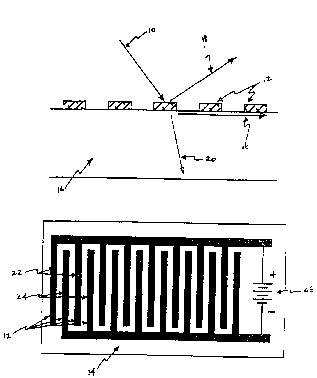
of FIGS. lA-lB. In FIG. lA, an external wave of light 10 is incident upon
10 a metal grating 12. The external wave 10 may be produced in a number
of ways. For example, the external wave 10 may be produced by a
separate source and then propagate through a homngPnPQus medium to the
invention, as might be the case if the invention were used to modulate the
separate source. AlL~ L;~ly, in the case of optical hlL~l~o~ , the
15 wave may be directed to the invention by optical elements such as a lens
or lens array, mirrors, diffractive optical elements, or a computer generated
hologram. Fibers may also be used to generate external waves as shown in
FIGS. 2A-2B. In FIG. 2A, the external wave 10 is directed to the grating
12 by an optical fiber 13. In an i..~.c~ g embodiment in which the
device is used to modulate a reflected wave 18, the same fiber 13 may be
used to generate the external wave 10 and to recapture the reflected wave
18. In FIG. 2B, the e~ternal wave 10 is a guided wave of the fiber 13 and
the cladding 13A of the fiber 13 may be partially stripped to allow the
grating 12 to couple the wave 10 from the core 13B. The term external
wave is meant to include but not be limited to waves generated by these
means. The term specifically excludes guided waves, such as TIR guided
waves and surface plasmons, which are guided by the structure of the
invention as described below. In addition, FIG. lA is not meant to limit
the invention to a particular spatial rPl~tion~hir between the external wave
10, the grating 12 and the substrate 14, which in this embodiment
n r~ o
a
WO 96/05536 - ' PCI/US95110313 i~
represents the ,~l,ld;"d~. of the device. For example, in FIG. lA, the
external wave 10 is depicted as en~u"~u~ g the grating 12 and then the
substrate 14. However, it is equally valid for the wave 10 to approach
from the substrate side, thus en~uullL~ling the substrate 14 and then the
5 grating 12. Other spatial cnmhin~tif~nc, particularly with regard to the
more complex embodiments described below, will be apparent to those
skilled in the art.
The grating 12 is fabricated on the surface of a silicon substrate 14
and the interface between the grating 12 and substrate 14 is capable of
10 supporting a surface plasmon 16 which p~ d~d~es along the two
structures. The external wave 10 is coupled by the grating 12 into
reflected waves 18 and transmitted waves 20, as well as the surface plasmon
16. Although these waves are indicated by single arrows, it is to be
understood that they may be a number of waves corresponding, for
15 example, to different d;rrld~ ~;o~ orders. In the preferred embodiment,
each stripe of the metallic grating 12 also functions as an electrode. The
electrodes 12 are electrically connected in an ;"~.d;~; d~el fashion,
forming first and second fingers 22, 24 and the electrical function of the
device may be achieved through these fingers. For example, a voltage may
20 be applied across adjacent electrodes 12 or the current flowing between
adjacent electrodes may be sensed. This dll U.~,~..ll~,.l~ of electrodes allows
for fast electrical operation of the device while ~ .".ng the optical
coupling function.
This and the majority of the following embodiments may be
25 fabricated via t~rhni~ Pc familiar to those skilled in the art. Such
tlo~hniqu.oc are described in standard sources such as Mayer, J.W., and Lau,
S.S., Electronic Materials Sciencefor Integrated Circuits in Silicon and
Galli?~m Arsenide, New York: McMillan (1990) and Sze, S M., VLSI
Technology, New York: McGraw-Hill Book Co., (1988), the teachings of
30 which are inco.~J.d~el herein by reference. Of the steps required to
WO 96/05536 219 7 3 2 8 PCT/US95/10313
fabricate the various embodiments of the invention, the ph~tolithc)graphy
step will often be the most stressing. For some applications, conventional
optical lithography may be used. However, in some cases the critical
~limPnci~mc of the device (e.g., the width of the electrodes 12) will be small
5 enough to require other types of lithography, such as electron-beam
lithography or x-ray lithography. For the remainder of this disclosure, the
methods for f~hri~ting embodiments of the invention will be omitted for
purposes of brevity except in cases where one skilled in the art would not
be familiar with the required f~hri~rinn
In the preferred embodiment of the device operated as a m~ tor,
the reflected wave 18 may be taken as the output wave. The reflected
wave 18 is chosen for illustrative purposes. The transmitted wave 20 or
the local wave 16 may also be chosen as the output wave. The strength of
the output wave may be mo~ tP~ by varying the efficiency with which
the incident wave 10 couples into the various modes 16, 18, 20. A
voltage difference 26 is impressed across the two sets of fingers ~, 24, thus
b~nc~ g an electric field in the substrate 14. By varying the voltage
difference 26, the electric field and hence the refractive index of the
substrate 14 may be changed, thus changing the coupling efficiency
20 between the input wave 10 and output wave 18. The specific ",PI l,~ "
which effects the change in refractive index operates as follows. Light is
absorbed in the silicon substrate 14 and produces electron-hole pairs which
change the refractive ind~ via the free-carrier plasma effect. The applied
voltage 26 may be used to sweep electron-hole pairs out of the substrate
25 14, thus varying both the number of electron-hole pairs l~.ll~lfillg and the
resulting index change. For a more detailed discussion of methods by
which an applied field may achieve a refractive index change in silicon, see
Soref, R.A. and Bennett, B.R., "Electro-optical Effects in Silicon," IEEE J.
Q~antum Electronics, QE-23, 123 (1987), the teachings of which are
30 incorporated herein by reference.
11
WO 96/05536 ~ ~ 9 7 3 ~ ~ PCTIUS95/10313 ~
The invention may also be used to detect light. In a preferred
embodiment, the voltage 26 is used to set up an electric field within the
substrate 14. The incident light 10 then generates electron-hole pairs and
this effect is enhanced due to coupling to the surfaoe plasmon 16. As a
5 result of the electric field, the generated electron-hole pairs are swept from the substrate 14 to the grating/electrode 12, and the strength of the
incident light may be d~t~llllhled by ~ ... ;"g the current which flows
between fingers 22, 24.
While the above discussion discloses a specific embodiment, it is to
10 be understood that the invention is not limited to this embodiment.
The following sections discuss the invention in more detail. In
particular, the next section discusses various aspects regarding local waves,
of which the surface plasmon 16 is one type. Different types of local
waves, the con~iti~nc required to support local waves, requirements for
15 coupling between an external wave and a local wave, and nonlinear effects
are considered. The following section discusses various methods regarding
the use of the invention as a mn~ t-)r Basic physical phPn~)m~n~ are
first described, followed by specific embodiments based on metal-
s~mi~t~nt~n~ror-metal (MSM) and lateral p-i-n (LPIN) structures. Other
20 potentially cignifir~nt effects, such as heating and possible operating
;~s are also considered. The section on the use of the invention
as a detector then follows. The last two sections are general illustrations of
some applications of the invention and a list of references.
25 2. Local Waves
In this section, different types of local waves and the structures
required to support them are first discussed, followed by l~luh~ on
grating couplers used to couple between an external wave and a local wave.
Finally, nonlinear effects of the local wave are considered.
12
219732~
WO 96/05536 PCI/US95/10313
2.1 Types of Local Waves
In an optical waveguide, light can propagate over extended distances
within a confined region due to total-internal-reflection (TIR) or surface
~ plasmon mode generation as described in Tamir, T., ed., Integrated Optics,
5 Berlin: Springer-Verlag (1993), the teachings of which are incol~o.d~ed
herein by reference. A three-layer dielectric which supports a TIR mode is
shown in FIG. 3. The local wave plu~d~;dLeS primarily in the film 28 as
indicated by the arrow and the refractive index of the film 28 must be
higher than that of both covers 30A, 30B in order for the local wave to be
10 confined in the film. The name TIR refers to the ray trace model for local
waves plO~dgd~ g in the film. In this model, rays which correspond to
guided modes are incident at either film 28 - cover 30A, 30B interface at
greater than the critical angle and are totally internally reflected back into
the film 28. The curve 34 illustrates a typical electric field for a low order
15 TIR mode. The TIR mode is the mode associated with waveguides such as
optical fibers, in which the core of the fiber corresponds to the film 28 of
FIG. 3 and the cladding l,Ull~JUlldS to the covers 30A, 30B.
Another type of local wave utilizes a surface plasmon mode (or TM
surface-wave) to propagate optical energy as shown in FIG. 4. In this
20 mode, the field ~lupd~,d~e~ along a single interface between a metal 36 and
a dielectric 38, as indicated by the arrow. The curve 40 illustrates a typical
magnetic field profile for a surface plasmon. Properties of surface
plasmons include high field lor~li7~ti~-n and large propagation losses due
mainly to absorption processes n the metal region. Preferred metals
25 include llnminllm, gold and silver. In order for a surface plasmon mode
to exist, the metal and dielectric must satisfy the condition
Re { [~M ~ M + ~,)] }~ Re {~5Yi} (l)
~ where ~M is the complex dielectric constant of the metal and ~, is that of
the dielectric. The surface plasmon osrill~tionc supported by an electrode
30 of the type shown in FIG. lA will have somewhat different excitation
WO96/05536 21~73~8 PCr/US95/10313 ~
cnn~litionc since the electrode is not a cl~ntimlollC sheet as is the metal 36
of FIG. 4. Nnn~thPlpcc~ the existence condition is similar in both cases.
Light may also be coupled to surface evdllescc~l~ modes, and TIR,
surface plasmon, surface evanescent modes or any cf~mhin~tion of these
5 types is d~ Upl;d~c for use in the current invention. However, in the
preferred embodiments disclosed below, the local wave will be either a
TIR or surface plasmon mode.
Since it is desirable to integrate electronic circuitry on the same
substrate as the invention, candidate materials include group IV systems,
lO m-v systems, and II-VI systems in general and silicon, silicon carbide,
AlGaAs, and InGaAsP compounds in particular. The majority of
embodiments will be discussed in the cont~t of silicon. However, the
invention is not limited to these materials and embodiments based on
materials such as electro-optic materials, electro-optic polymers and related
15 organic materials, or phu~olcrldc~ are within the scope of this
inventiom
Waveyuide CQU~
In the invention, the ~ternal wave is coupled to a local wave. In
20 ûrder tû do this, the Wd~ Ol ûf the incident light, k, must be phase-
matched with 1~, the real part of the propagation Wd~ Ul of the local
wave. This is achieved by the grating and the phase-matching condition is
,B = k sine + 2~mT (2)
25 where e is the resonant input coupling angle, T is the grating period, and
m is an integer which represents the diffraction order coupled to the local
wave. For ~ample, the first-order diffraction from the grating will couple
to the wdvc~ dc if jml-1 and the second order when Iml-2. In some
applications, the light may be preferred to be normally incident to the
30 electrodes with e=o. In the current invention, the required grating is
14
2 ~
~ WO 96/05536 pCr/US95/10313
formed by the placement of the electrodes. Since the grating period will
typically be on the order of a wavelength, the width of the electrodes will
also typically be on the order of a wd~ ,Lll. For example, in the near-
infrared region, the electrode width will typically be on the order of
5 several tenths of a micron.
While equation 2 is cast in terms of a grating of constant period, in
reality, the coupling device may be aperiodic. For example, if the external
wave is irregular in its intensity or phase profile, the electrodes lie on a
non-planar substrate, or the required coupling efficiency varies with
10 location, then the electrodes may be placed in a regular pattern which is
not strictly periodic.
There is a symmetric relation between coupling into and out of a
waveguide. To be more specific, a grating couples energy out of a
waveg ude as well as into it and this coupling is not 100~h efficient. That
15 is, it typically takes many interactions between a wave and a grating before
a ~Igmfi~nt amount of the hght IS elther coupled mto or out of a
waveguide. The coupling effficiency of the grating also depends on a
number of other factors: the grating and wd~,uidc geometry, the profile
of the incident beam, and the indices of refraction of the materials
20 involved to name a few. By varying any of these factors the coupling
effficiency may be varied.
2.3 Nonlinear Effects
Related to the topic of grating coupling are effects imposed on the
25 behavior of the system due to nonlinear processes. In the context of this
invention, the primary nonlinear processes involve changes in refractive
index due to free carrier density and/or t~ ?CId~ changes within a
sPmi~-~n~ ctcr-based material structure. These effects are described in
Preallots, D.F. and Brown, T.G., "Optical Limiting and Free-Carrier
30 Dynamics in a Periodic S.omi~ ctnr Waveguide," ~. Opt. Soc. Am. B.,
~=:
~1~732~ ~,
WO 96/05536 PCT/US9',/10313
11(2), 304-312 (1990), the teachings o~f,w~hich are incorporated herein by
reference. The nonlinear ref~active index may be lc~lu,c.!L~d as
n(NcT) = nO + ~nNL(Nc, 11 ( )
5 where nO is the linear refractive index, Nc is the free-carrier density, T is
the tC~ .d~ulc~, and ~ is the nonlinear contribution to the refractive
index. Changes in Nc and T are brought about primarily by optical
absorption or by carrier injection.
The propagation index ,6' in both the three-layer and the two-layer
10 waveguide structures of FIGS. 3 and 4 depend strongly on the refractive
index of the film 28 or dielectric 38, lc~ ly. Given the nonlinear
nature of the coupling structure, a more accurate Iq~lc~ Ld~ion of the
phase-matching condition of equation 2 would be
e(~nNL) ~ sin [~ nNL) - 27rm/T] (4)
15 Therefore, changes in e due to nonlinear changes in the refractive index
directly affect the phase matching condition. FIGS. 5A-5B illustrate this
by plotting the strength of a reflected wave versus the incidence angle e.
FIG 5A illustrates a device designed for m~imnm reflectivit,v at
resonance, while F~G. 5B is a device designed for minimum reflectivity.
20 At the resonance angle ~ energy couples from the extern21 wave into
the local wave, resulting in a ~ ibu~ion of energy among the various
waves and a change in the strength of the reflected wave. The nonlinear
shift in ~ is d~7plu~hlld~1y proportional to the change in index Qn.
In addition to the nonlinear detuning effects imposed on the
25 resonance, a nonlinear refractive index can also lead to interference effectsint he coupling region of the ~ ,u;de. Typically, the external field does
not couple into the local wave at only one point. Instead, coupling takes
place over a relatively broad region (compared to the grating period) of the
grating in the direction of propagation of the local wave. Therefore, given
16
~ WO 96t05536 2 1 ~ 7 ~ 2 8 r ~ ~5, i'~?l3
the spatial nature of the coupling process, there is also a spatial ~IPpPnr~Pnrewhen c~-nci~lpring the nonlinear effects. Assuming this, the nonlinear
propagation Wd~ JI can be written as ,B(z) = ,~[AnN, (z)], where z is
taken as the direction of propagation of the local wave. Hence, at each
5 point in the z-direction along the grating, the coupled light has a different
phase relation that is ~;epPn~Pnt on the nonlinear term of the refractive
index. In addition to the initial coupled phase term, each spatial
~ol.lpollcl,~ of the local wave ~rcllmnl~r~c a propagation phase term
relative to the coupled incident field. As a result, for any given point
10 along the propagation path, interference effects between the pl~)pd~,dLlllg
local wave and the coupled incident field can take place if the phase
difference is large enough. Any light coupled out of the waveguide may
P~pPriPn~e either ~ullaLlu~ive or destructive interference over the coupling
region, corresponding to either a high or a low measured reflectivity along
15 the propagation path.
While both nonlinear coupling effects described above (resonant
detuning and traveling-wave LlL~lLl~ e interactions) may be used in the
invention, the invention is not limited to these effects. For example, one
embodiment may use electro-optic materials to fill the spaces between the
20 electrodes. As the voltage between the electrodes is varied, so will the
refractive index of the electro-optic material and the coupling efficiency of
the grating formed by the electrodes and the material. Furthermore, the
electrodes ~L~lllsel~ may be ~l~ula~.u~ (e.g., indium tin oxide) and so
the grating coupler may be a phase grating rather than a metal grating.
25 While it is intended that these embodiments lie within the scope of the
!
~ a7328
wo 96/05536 ~ l ~ r~ 3
invention, the preferred embodiments described herein will rely on
resonant detuning.
3. Modnl~tion
This section considers the operation of the invention as an optical
mr~d~ tflr. The basic operation is further discussed and then two specific
embodiments, one based on metal-sPmi~onfluctflr-metal structures and the
other based on lateral pin diodes, are disclosed. Although the discussion is
in the context of mod~ tflrc, those skilled in the art will recognize that
the teachings are not limited to mo~ tors For example, they may be
applied also to the invention used as a detector.
3.1 Basic Physical MP~h~nicmc
In preferred embodiments of the invention which are used as
modlll~tors, the morllll~tif n of the output wave is effected by varying a
voltage placed across adjacent electrodes which, in turn, results in a
refractive index change in the wave gui&g structure. This then r~sults in
a change in the coupling between the external wave and ~he local wave via
the processes described in 2.3 and a sllhsPqllPnt mf~ tion of the output
wave.
In generaL the physical ~f. ~ ll underlying the mr~ tifm does
not have to depend on a refractive index change. The absorption
coPffifiPnt or l,h, r, ;,.~ Cf~ of the device are two common alternate optical
parameters which may be used. Furthermore, in the preferred
embodiment, the applied voltage changes the refractive index primarily via
the free-carrier plasma effect. The invention is not limited to this effect
and an electric field may be used to change the optical properties of a
material by any of the following Il,f. h.ll~ .C to name a few: the Pockels
effect, the Kerr effect, the Franz-Keldysh effect, the quantum confined
Stark effect, and band-filling.
18
21~7~28
wo s6toss36 r~ 7~lr~l3
For the preferred embodiment with a silicon substrate, the free-
carrier plasma effect is used. This is an cle~LlvlLdction process by which
the refractive index is modified by the introduction of free carriers. The
carriers are normally introduced either by direct current injection via the
S electrodes or by phoLogrl.cldLion of carriers in a sPmirr,rJ~ rrc)r material.
The change in ind~ is then induced due to plasma interactions between
the carriers and the optical field. This mPrhqnicm is suitable for both
. .
dlrect and mdlrect bandgap materlals, mcludmg slhcon.
3.2 MSM Devices
A preferred embodiment of the invention relies on metal-
sPmirr~n~nrror-metal (MSM) structures. Referring to FIG. 1, if the
electrodes 12 are metal and the substrate 14 is a sPmi~r~n~lllrtnr~ then
FIG. 1 depicts such a device. In the preferred PmhorlimPnr, the substrate
14 is silicon. If the Ll~u~slLu--ed wave 20 is the desired output wave, then
the substrate 14 may be replaced by a silicon ul~lubl. uc in order to reduce
the qttPm~qtion of the ~l~llu~Led wave 20. As described in section 2, the
electrodes 12 are spaced so as to couple the external wave 10 to the local
wave 16, which is a surface plasmon in this specific e~ uldLion~ and the
coupling effficiency is varied by varying the refractive index according to
the nonlinear effects described in section 2.3.
More specifically, as shown in equation 3, the change in nonlinear
refractive index for a cPmicr~nrlllrtor is a function of both carrier density
and ~e~U~ UlC. Each of these contributions can be separated out so that
~nNL~c,T) = ~c + ~\nT (4)
where nc is the refractive index change due to the carrier concentration
and ~nT is the change due to ~LU~c.d~ul~ Using Drude's theory to model
~ the carrier dynamics, the electronic contribution to the refractive index
may be modelled via Drude's model as described in Blakemore, J.S., Solid
St~te P~ysics, 2nd ed., ~'.amhri~lgP (~qmhril~gP University Press, 157-169
19
n
o
WO96/05536 ~ ',' .' ~ PCI/US95110313 --
(1985), the teachings of which are incorporated herein by reference. The
refractive index then has the form
~ nc = Nc (-8.9 x 10 2cm3) (5)
FYrf-rimPnt~lly, it has been shown that the thermal contribution can be
d~pl VlL;llldLe :I by
~ nT = ~ - 300K) (2 x 10~ K-') (6)
See Sauer, H., et al., :Optimi7.~tirln of a Silicon-on-Sapphire Waveguide
Device for Optical Bistable Operation," J. Opt. Soc. ~4m. B., 5(2), 443-451
(1988), the teachings of which are incorporated herein by reference.
10 However, in the preferred embodiments, it is desirable to minimize
thermal effects for several reasons. First, the thermal processes are
typically much slower in their response times than the electronic effects.
Second, equations 5 and 6 have opposite signs and tend to cancel each
other when both are present. Hence, to design a fast and efficient optical
15 switching system, the effects due to ~ dLul~: should be l,l;.~; ";,~.
( ( n . . 1l l Ig on the electronic effects predicted by the Drude
theory, there are two ways in which the carrier density can be modified in
the MSM structure. They include either carrier-injection or carrier
geueration via optical dt~svl~L;on~
If the interior of the Srmi~ o~ -- region is assumed to be ohmic,
then the result of carrier-injection (or injected-current) can be modeled by
Ohm's law which states
J e a E, (7)
where J is the internal current density, E is the internal electric field, and a25 is the conductivity which is proportional to the carrier concentration. Nc.
At any given instant in time, carriers are injected into the crmirr,n~ ct-~r
region between the electrodes resulting in a change in the refractive index
as predicted by Drude's theory.
The other method uses the crmirrlnrlllrtr,r's absorption properties to
30 generate carriers. If the incident optical energy is equal to or larger than
~WO 96/05~36 2 1 ~ 7 ~ ~ ~ PCTIUS95/10313
the S--micon~llrtnr's bandgap, then cl~.L~ i~ in the valence-band can
absorb sufficient energy to be transported into the cnn-hlrtinn band. The
free-carrier concentration may be changed either by changing the strength
of the incident light or, as is the case in the preferred embodiment, by
5 changing a voltage applied across the electrodes to sweep carriers out of the
5Pmir-mrlllrtclr region. One absorbed photon creates one free electron-hole
pair. The absorption process for direct bandgap ~rmirr~n~lllrtors such as
GaAs is a one step process, while the process for ~rmi~rlnrlllrtrr~ with ==
indirect bandgaps such as Si requires two steps. In indirect bandgap
materials, the absorbed photons do not provide a change in mrlm~ntllm,
and a second process is required to transfer e~/:cited electrons into the
cr~n~lllrt;on band. This usually involves the emission of a lattice phonon.
Due to the second absorption step, resonant absorption in indirect bandgap
5rmirnn-1llrtor5 is typically much smaller than s~ mirrlnrlllctrrs with direct
bandgaps.
One advantage of the ph(llo~hsol~ion approach over the direct
current injection approach is that ph.~Lolh~ Li~/~ devices will potentially
require less power since the energy to create the free carriers comes from
the incident light and not from current generated by the device itself.
3.2.1 Electronic PlopclLi~s
The preferred method of varying the carrier ~O~ ,lLLdLion may be
understood by cnnCiflrring the electronic properties of the sPmirnn~hlrtnr-
metal interface. FIG. 6A is a simplified one~limrn~inn~l model of the
electronic state of the MSM device of FIG. 1. The fingers 22, 24 and the
5lomil.,n~ .1 14 form two interfaces 42A, 42B. At each interface 42A,
42B, a depletion region forms, which is known as a Schottky barrier.
FIG 6A illustrates this in the energy diagram 44 of the MSM structure
with zero-bias. Here Ec is the Srmirrln~uctnr cr/n~lllrtinn band energy
level, E~ is the ~rmifnn~lllrtnr valence band energy level, and Ef is the
21
W096/05536 ~g7~ ~ PCT/US9~10313 ~
Fermi energy level for both the metal 22, 24 and the s~mirt-nf~ tor 14 at
zero-bias. For n-doped sPmi~onrl~ rc, e~cess carriers migrate into the
metal region due to lower energy states in the metal. As the carriers
vacate, the charge imbalance between the regions generates an electronic
5 field that eventually :~U~)~JlC~ CS all current flow. This forms the ba~sis ofthe Schottky barrier. If the barrier is large enough, and if there is no
incident light, current flow is ~u~lca~cd even when an applied bias voltage
is present. Hence, a Schottky barrier behaves electrically like a diode.
This property is what allows it to be used as an optical detector or
10 mr~ t~r,
As discussed previously, energetic photons absorbed in
5Pmif/-n-lllctrlrc will generate free-carriers. In an MSM structure with zero-
bias, the generated frcc-cle~Llulls 46 tend to ~rcnmlll~tP in the
sPmif cn-lnctor region between the metal electrodes 22~ 24. This occurs
15 due to the symmetric bending of the c~nrl~lrtir)n band at the
SPmi~ ~-n-lllrtor-metal interface. Generated holes 48 on the other hand tend
to migrate towards the interface 42A, 42B due to valence band bending.
In the preferred embodiment, the pooled free-carriers are swept from the
5Pmifrm~lllctnr region, thus changing the carrier density and leading to a
20 corresponding change in refractive index. The sweeping is achieved by
applying a bias 26 across the metal electrodes 22, 24 of the MSM structure,
as shown in FIG. 6B. Here Efs and Efm are the Fermi energy levels for the
sPmi~nrluctclr and metal regions, l~ ly. As shown, one interface of
the structure is reversed biased while the other is forward biased. The bias
25 voltage shifts the respective Fermi energy levels at each interface. This
results in a tilting of the c~-n~inrtirm energy band allowing the electrons 46
to spill through the forward biased region, thus changing the carrier
c-~n~ Pntr~ti~n
The process described above is for m~ ting light using optical
30 absorption to induce refractive index changes. It does not cover carrier-
22
21 97~2~
WO 96/05536 ~ 13
injeaion. However, carrier-injection mn(~ tinn is conceptually a simpler
process to describe. To modulate with injeaed carriers, the bias 26 is
made large enough to overcome the Schottky barrier potential. This
~ results in an increased current flow through the s~mirnn~ ctor region 14,
5 which correspondingly changes the inct~m!ln~Qll~ carrier density and
coupling properties. However, this method of mn~llll~tinn would typically
be reserved for MSM structures having small Schottky barrier contaa
potentials. That is, the metal-c- mifnn~llanr interfaces 42A, 42B should be
ohmic contacts.
10As a final observation, it should be noted that the metal elearodes
12 serve two purposes. First, they serve an optical function in that they
couple the external wave 10 to the local wave 16 and also form a structure
which supports the local wave 16. Second, they serve an electrical
funaion in the formation of the Schottky barrier 42A, 42B and the
15 application of a bias to the barrier. A single metal may not be ideal for
both functions and so the elearodes 12 may have a ~Olll~O~;~e struaure.
For exarnple, gold is a preferred metal for the support of surface plasmons.
However, it does not form a good Schottky barrier, while tungsten does.
Therefore, the elearodes 12 may consist of a tungsten layer in contaa
20 with the silicon 14 in order to form the barrier followed by a gold layer in
contaa with the tungsten in order to support the surface plasmon 16. In
general, the elearodes and the u Id~.lyhlg struaure may be even more
complex, including the use of doped c~mi~on~ tnr regions, quantum well
structures, superlattice structures, and ~.dn~ ,.n ctm~hlctor~ such as
25 indium tin oxide. For example, quantum wells and quantum wires may be
used in the Sf.~ r region 14 in order to increase the effective
carrier density and enhance the field-induced change in refraaive index.
23
~197328, ~
W096105536 '' '. ~ ' pCT/US95110313
3.2.2 Cover Material
The MSM structure of FIG. 1 is highly asymmetric. In essence,
there is a large refractive index gradient between the air, which may
generally be considered a cover layer, and the metal 12 and sPmironrl1lrtr,r
5 14 layers. As a result, the cover coupling efficiency into the structure can
be poor as illustrated in FIGS. 7A-7C, which show the profiles of three
possible surface plasmon modes 49A, 49B, 49C. In the MSM structure
there are tWO interfaces where plasmons are generated. One is at the
cPmiron~ rtrlr 14 - metal 12 interface and the other is at the air - metal 12
10 interface. For the asymmetric structure, there is very little overlap
between the plasmon modes of the two interfaces. This results in a low
energy exchange between the modes, and poor cover-coupling into the
sPmirc-nrlllrtor 14 -metal 12 plasmons. Sinoe the switching processes
utilized in the preferred embodiment occur within the sPmirr~n~ rtor
15 region 14, an hllplo~,ll~lL in the overlap between the plasmon modes will
result in improved device p . r~ re In the preferred embodiment, this
is ~rr~mrlichP~I by symmPtri7ing the structure by depositing a layer 50 as
a cover. The cover 50 is chosen to have a refractive index ~pplu~ L~ly
equal to the Spmiron~llctrlr layer 14. Preferred materials include
20 amorphous and poly-crystalline silicon although materials are not limited
to these choices. Other tliPlPrtrirc thin films and even organic materials
may also be used. This creates a buried electrode-coupling structure, as
shbwn in FIGS. 7D-7E. The additional layer improves the plasmon mode
overlap, as illustrated by the mode profiles 51A, 51B, resulting in better
25 cover-coupling into plasmons generated at the sPmirrm~ ctc)r 14 -metal 12
interface. Although the use of a cover material is illustrated in the context
of the MSM embodiment, it should be understood that this general
principle may be applied to other embodiments as well.
~ WO 96/05536 2 ~ 9 7 3 2 8 PCTIUS95/10313
3.2.3 Multi-layer Devices
Although the invention has been discussed in the context of a metal
electrode on a bulk cPmirrnrl~lrtor substrate, it is not limited to this
~Onri~,uld~ion. An alternate embodiment involves using a three-layer
5 dielectric waveguide structure as illustrated in FIG. 8. The structure is
similar to that depicted in FIG. 3, and many material systems may be used
to fabricate the structure. However, silicon-on-insulator (SOl) structures
are preferred due to their ease of f~l-rir~ti/ln and the tight r~nfinPmrnt of
the local wave which results from their use. The SOI structure has a
10 number of different variations, which include silicon-on-sapphire,
separation by impl:lntPd oxygen, bonded and etch-back SOI (13EB-SOl~, --
and ploy-crystalline SOI. BEB-SOI has been shown to possess good
wd~c~uid;llg properties. Evans, A.E. and Hall, D.G.,''Mea~u~ llL of the
Electrically Induced Refractive Ind~ Change in Silicon for Wavelength
)~-1.3 ~m Using a Schottky Diode," Applied Physics Letters, 56, 212 (1990),
the teachings of which are hl~vlyold~ed herein by reference. In a preferred
embodiment of FIG. 8, the TIR wave is supported by an arnorphous
silicon cover 30A, a crystalline silicon film 28 and a silicon dioxide
insulating layer 30B. Metal electrodes 12 are used for coupling and
electrical functions. The entire structure is on a silicon substrate 52.
The three-layer structure of FIG. 8 has several ddVdUI~ ,S over a
bulk structure such as that of FIG. 1. It provides faster switching since
generated or injected carriers are restricted to a narrower region of the
5PmirrJn~ rtnr 28. In the bulk case, carriers can extent far from their
point of origins, resulting in a lagging of the tail-end switching response.
Second, both plasmons and TIR waveguide modes may exist in the
structure. The Cimnlt:~n~rlus excitation of both modes can lead to more
effficient mrdnl~tirn Compared to surface plasmons, TIR modes occur
deeper within the sPmi~ O~ 1 Iayer. As a result, more free-carriers are
liberated to affect the refractive index. In addition, when the structure is
2 1 9 7 3 2~8 PCIIUS9~110313--
WO 9610~36
brought into resonance during its low-reflectivity-state (off-state), more
energy may be coupled into the structure due to the added effect of both
modes. There arç also some disadvantages to the three-layered MSM
waveguide structure. The structure is obviously more complçx, both to
5 design and to fabricate. Additional leakage current due to a non-perfect
insulator 30B could result in added heating of the structure.
In the alternate multi-layer structurçs of FIGS. 9A-9B, quantum well
get~mrtriPc may be used to increase the effective carrier density and
enhance the field-induced change in refractive indçx. In FIG. 9A, the
10 insulating layer 30B of FIG. 8 is replaced by a quantum well structure
53A. In FIG. 9B~ quantum wires 53B are used instead. Normal
cl~Llvabsol~Lion requires that the applied field be directed across the
quantum well, which is impractical in the çmbodimçnts of FIGS. 9A-9B.
However, it is possible to make use of rrm~ rir~n along the quantum well
15 in order to increase the effective current density associated with carrier
injection. This would result in far lower injection currents. m-v systems
such as AlGaAs and group IV systems such as SiGe or SiC are preferred
material systems for such .omho~lim~.nt
Many other variations of multi-layer structures will be apparent to
20 those skilled in the art.
3.3 LPIN Device
An alternate preferred c.llbo.l;~ is shown in FIG. 10. The
crystalline silicon film 28 and buried oxide layer 30B on the silicon
25 substrate 52 are similar to the SOI structure of FIG. 8. However, the
remainder of the structure is more complçx. The metal electrodçs 12 are
separated by a top oxide layer 30A and alternatçly contact p+ and n+
doped regions 54, 56, thus forming a lateral periodic seriçs of PIN diodes
(also known as a LPIN structure) on a silicon-on-insulator (SOl~ structure.~0 The doped regions may be formed by deposition, diffusion or a
26
~ wo 96/05s36 2 1 9 7 3 2 8 p~ 0à13
cnmhin~ti(m of the two. With a modest reverse bias voltage, the depletion
region extends fully between the p+ and n+ diffusion regions 54, 56. A
feature of the design is the buried oxide region 30B. This attribute
prevents the generation of deep carriers during the absorption process,
which would otherwise li_it the bandwidth of the device.
One advantage of this design over MSM is the high quality junctions
that exist at the n+-n and p+-n diffusion interfaces. Since the base
materials are all silicon, there are fewer defects and fliclor~tionc at the
bolm-~riPc This results in lower leakage and longer free-carrier lifetimes.
In the preferred embodiment, the PIN diodes are operated in forward bias
and morl~ ti-m of the refractive index is achieved by current-injection.
Like the MSM device, the electrodes 12 of the LPIN can act as a
waveguide coupler. However, it is difficult for the LPIN structure to
utilize optical-plasmon interactions due to the lack of metal surfaces within
the depletion region. However, since the structure is in the form of a
,LL~ lay~l dielectric (SOl), TIR waveguide modes could be used instead.
To improve the cover-coupling efficiency of the structure, a high-index
cover layer may be added as discussed previously.
3.4 Mic~Pll~nP~Illc Consider~tionc
In addition to the optical coupling and electronic operation of the
device, several other ~.n~ )nc are worth mPnti~ning
3.4.1 Thermal Chd-J 1~
As shown in equation 4, the total change in index is the sum of
both electronic and thermal processes. One main consideration when
designing any kind of uL~u~ ullic structure is the impact of device
~ heating. As pointed out previously, thermal effects have â much slower
response time compared to electronic processes. As a result, if the
dominant physical effect is thermal, the mo~ ti~.n switching speed can be
27
21~7~28
W0 96/05536 r.~ 511~ ~13
seriously degraded. Another problem exists due to the opposite signs of
the thermal and electronic effects. Since the total index change is the sum
of these two quantities, thermal index changes tend to cancel out the
electronic index changes. Typically, thermal changes should be minimi7rr
5 Standard methods include the use of heat sinks or active coolers with
feedback loops to maintain the thermal stability of a device.
One source of heating is the nollldd;dlivr l~ r.",h;.. ~ 7n of
generated electron-hole pairs in the ~rmirQnrlllrtQr region. When optical
energy is absorbed, creating pairs of electrons and holes, the individual
particles migrate in directions according to the local field distribution. The
generated particles can be used in either modifying the refractive index for
mf~lnl~tirln or generating a photo-current for detection. However, if the
electron-hole pairs recombine nomd~l;d,i~'y before their properties can be
used, the stored energy is given up to the srmirrlnrlllrt~r lattice in the
form of heat. It should be noted that indirect bandgap Srmicrn~llrtors
have not allowed radiative transitions, which means that all free-carriers
must decay nolllddidLi~ly. However, the carriers can be swept from the
interaction region with an applied electric field before rec.~mhin~tirln takes
place, thus reducing the heating effect.
A second source of heat is Joule heating which arises from a
srmiron~urtrlr's resistance to current flow. When current passes through a
material, inelastic collisions occu-r between the flowing electrons and the
lattice. This generates heat throughout the material. Joule heating occurs
for both current-injection and photo-generation cases. However, assuming
equivalent electronic effects, Joule heating from current-injection is the
more ~lulllh~.lL of the two. When free-carriers are photo-generated, they
are trapped inside a potential well with no net current flow and hence no
Joule heating. Current flows only when a field is applied across the region
of generation. Hence, the photo g~ dL~d carriers experience a shorter
resistive path during the sweeping process resulting in less heat generation.
28
21~7~28
WO 96/05536 . ~,111J.,,31'' 1~
One method that may be employed in c-7mhArin~ the Ltlllp~ld~u
effects, is balancing the thermal generation processes during the on- and
off-states (or high- and low-reflectivity-states) of the ml~nl~tcln In essence,
it should be possible to achieve a thermal pseudo-steady-state, thus
5 ~ ;IIg time--iPrenrlPnt ~lu~la~ult effects.
This process of balancing the temperature during the on/off-states is
applicable to the MSM-m~ r concept utilizing photo g~lleldLcd
carriers. Unlike the current-injected m~ tor, a large density of photo-
generated carrier exists within the structure during the on-state. As we
10 pointed out earlier, the generated free-carriers recombine n~lnA~ y
due to current leakage, thus, heating the lattice. During the off-state of the
mn~ tor, current flows through the structure causing Joule heating.
Therefore, if the amount of heat generated from recomhin~ti--~ and
current flow are equal, then time-~lPrPnrlPnt thermal effects are ...;..i",;,~
3.4.2 Wavelength of Operation
The wd~l~gLL range over which the mn~lnlAt~-r will function is
another important ~..n~ n For the preferred embodiment based on
silicon, the optical absorption is d~p~ hlld~ely 11 cm-l at a wd~ ,LL of
20 1.06 ~m. At this wd~ Lll at room telu~eldLul~ the photon energy is
d~pl~ L~ly equal to the bandgap energy of silicon (1.12eV). If the
wd~ ,Lll becomes longer than this, then the absorption rapidly
decreases. At shorter wd~ ,Llls, the absorption increased rapidly. The
absorption curves are different for crystalline, poly-crystalling, and
25 amorphous silicon. Amorphous and ploy-crystalling silicon are mPnti~nPrl
since they may be used as cover materials to ~yllllu~ the structure. As
the absorption increases with shorter wd~ ;LLs, the rate of free-carriers
generation in silicon also increases. Therefore, in ~omhorlimPnt~ which rely
on the photo-generation of carriers, operation of the device at shorter
30 wd~lcll~,Llls may improve the ml rllllAti~)n strength of the device.
29
7 ~
WO 96/05536 PCI/US95110313
4. Detectors
Embodiments which are used as detectors largely rely on similar
phPnnm~n~ as those which are used as mn~ tors. For example, a
mnd~ tnr may be thought of as a device which controls the coupling
5 between the external wave and the local wave by varying the voltage
across the electrodes. This is achieved because varying the voltage affects
the number of free carriers produced in the 5~mirnn~ tnr waveguide, and
the number of carriers affects the coupling by changing the refractive index
of the waveguide via one of the clc~n~l~rld.Liv~ processes. In short, the
10 electrical state of the electrodes affects the number of carriers which affects
the coupling of light. A reversal of this chain - light affects the number of
carriers which affects the state of the electrodes - roughly describes the
detection process. The device is ~unrl~,ultd to maximize the coupling of
the external wave to the local wave. The m:l~imnm strength local wave
15 then produces carriers in the ~ "~ h~tor material which are sensed
through the electrodes. Hence, many of the teachings for mn~ tnrs are
directly applicable to detectors also and the embodiments, including the
preferred ones based on the MSM and LP~ structures, may be used as
detectors. The following sections highlight only the differences between
20 embodiments intended to be used as detectors and those intended to be
used as mn~ rors
4.1 Wavelength of Operation
In the mo~ tcr, the absorption ~Ldud~Ltl;~ic of the device
t~rmin~ the number of free carriers generated by phnto~hsnrption.
However, in cases of weak absorption, free carriers can be generated by
the alternate process of direct injection. In the case of detection, this is
not so. The device is restricted to wd~lc.l~;Llls for which the device
absorbs the incident radiation and stronger absorption translates directly to
30 a more sensitive detector. It should be noted that the absorption process is
2 i 97~
WO 96/05536
not restricted to transitions from the balance band to the cnnfhlrtion band
of the Srmirnn~llrtor. For example, absorption may take place via a
transition from the metal Fermi level to the rnn~llctinn band of the
5!~micnn-1nctor.
.2 ~)etection M~?rhani~mc
The invention of the current device lies in the dual use of the
electrode structure. The electrodes optically couple light from the e~ternal
wave to the local wave and the strength of this local wave is then
10 electrically sensed via the electrodes. The optical coupling results in a field
which is enhanced with respect to conventional, uncoupled detectors, and
the s~lhsPqn~nt sensing of this field may be achieved by any of the
commonly used ph~to~lrtrrtir~n methods, including dl,~.udl~ej based on
phntoflin-l.os photocnnl~llntive devices and photovoltaic devices.
As e~plained previously, in the MSM approach, the double Schottky
barrier forms a pool of carriers and the application of a voltage bias then
tips this pool p.udu lug a current flow. In the detector application, the
voltage bias may be applied and the resulting current flow, which is
indicative of the strength of the external wave, may be sensed thus
detecting the strength of the optical field. Alternately, if the Schottky
barrier is low (i.e., the metal-~emifnnrlllctor contacts are essentially ohmic),then the resistance of the ~l~mi~n~lnctor will be .~. t. . ",h-.~,l by the
strength of the optical field and the device may be operated as a
, phntocnn~nntnr.
In the case of the LPIN structure, the device may be operated as a
conventional photodiode, either in the photoconductive or the
photovoltaic mode. In the photocnn~ tive mode, the pin junction may
be reverse biased and the strength of the external field ~irlr~ r(l by
sensing the current which flows through adjacent electrodes. In the
photovoltaic mode, no voltage is applied across the electrodes. Instead, the
31
2197328
WO 96/05536 . '.~ i ' ", PCT/~IS95ilO313 _
voltage resulting from carriers generated by the external wave is sensed,
thus indicating the strength of the external wave.
5. General Illustrations
A general illustration of the invention used as a m~-lnl~tnr is shown
in Figs. 11A - 11B; while Fig. 12 depicts the invention as used as a
detector. In Fig. llA, the invention is used in a reflective mode. The
external wave 10 is incident on the grating/electrodes 12 and the strength
of the reflected wave 18 may be varied as disclosed previously. In many of
the discussed embod;~ .lLs, the electrodes 12 lie on a silicon substrate 14
so conventional circuitry 58 may also be integrated on the same substrate
14. This circuitry 58 may be used to drive the electrodes 12 thus varying
the strength of the reflected wave 18. Due to the use of standard
t~rhnir~ oc in f~hri~ting both the m~ tQr and the circuitry, many
mndnl~tnrs or arrays of mn~ tnrc may be fabricated on a single
substrate. Fig. 11B shows a device used in ~ ;n~ In this case, the
1. ."~ wave 20 is the wave of interest which is mn~ t~ If the
light lies in a part of the spectrum for which silicon is highly ab~u~LuLi~, it
may be necessary to thin the silicon 14 or to use a silicon membrane for
the device and the circuitry 58. Structural support may be achieved by
using a glass or other transparent substrate 60.
In Fig. 12, the device is used to sense the strength of the external
wave 10. In this case, no waves are actively being mo(lnl~t~l Rather, the
optical field of the wave 10 produces and electrical effect which is sensed
by the circuitry 58 via the electrodes 12. The circuitry may also
incorporate more cnphicti~t.-rl functions such as local averaging, edge
detection and bd~ uulld corrections.
What is claimed is:
32