Note: Descriptions are shown in the official language in which they were submitted.
219? 62'~
-1-
Title: ANTIFUSE BASED ON SILICIDED SINGLE POLYSILICON
BIPOLAR TRANSISTOR
FIELD OF THE INVENTION
This invention relates to programmable antifuses and to
methods of making the same.
BACKGROUND OF THE INVENTION
Antifuses have been known for some time and are disclosed
for example in U.S. patents 3,191,151; 3,742,592; 5,019,878; and 5,298,784.
Antifuses are devices which have a high impedance before programming
and a low impedance after programming, and are used widely in
integrated circuit structures. An antifuse is the converse of a fuse, which
can be employed in a similar manner. Use of an antifuse permits the
tuning of various analog circuit parameters, the programming of digital
logic, and the selection of certain pieces of redundant circuitry. An
exemplary application for antifuses (given by way of example only) is to
switch desired resistances into a voltage controlled oscillator (VCO), so that
the center frequency and range of the VCO will be within desired
specifications.
Antifuses can be formed from transistor or diode structures
which normally have a high impedance when reverse biased. The
appropriate PN junction of the device can be shorted by applying a large
reverse bias, causing part of the junction to melt and causing the metal
which contacts the junction to flow into the molten region, thereby
creating a low impedance metal filament.
Conventional antifuse structures typically require a relatively
high programming voltage and energy, which may cause damage to the
remainder of the integrated circuit in which the antifuse is located. It is
therefore an object of the invention to provide an improved antifuse
structure, and a method of forming an antifuse, which require a lower
programming voltage and energy than have typically been the case in the
-2-
past.
BRIEF SUMMARY OF THE INVENTION
Accordingly, in one of its aspects the invention provides A
method of making an antifuse comprising:
(a) selecting a single polysilicon bipolar transistor
comprising:
(i) a collector layer,
(ii) a base layer overlying said collector layer and
having an upper surface,
(iii) an emitter structure overlying said base layer, said
emitter structure projecting above said base layer
and having a sidewall extending above said base
layer, said emitter structure also having an upper
surface,
(iv) a narrow oxide spacer ring surrounding said
sidewall of said emitter structure,
(v) a first conductive silicide layer on said upper
surface of said base layer, surrounding said spacer
ring, and a second conductive silicide layer on said
upper surface of said emitter structure,
(b) applying a pulse between said first and second
conductive silicide layers to form a filament between
said first and second conductive layers, said filament
extending from said second conductive layer down said
sidewall of said emitter structure and under said spacer
ring to said second conductive layer.
In another aspect the invention provides an antifuse
comprising:
(a) a silicided single polysilicon bipolar transistor structure
comprising:
(i) a collector layer,
219' ~ ~'~
-3-
(ii) a base layer overlying said collector layer and
having an upper surface,
(iii) an emitter structure overlying said base layer, said
emitter structure projecting above said base layer
and having a sidewall extending above said base
layer, said emitter structure also having an upper
surf ace,
(iv) a narrow oxide spacer ring surrounding said side
wall of said emitter structure,
(v) a first conductive silicide layer on said upper
surface of said base layer, surrounding said spacer
ring, and a second conductive silicide layer on said
upper surface of said emitter structure,
(b) and a conductive filament extending between said first
and second conductive layers, said filament extending
from said first conductive layer down said sidewall of
said emitter structure and under said spacer ring to said
second conductive layer.
Further objects and advantages of the invention will appear
from the following description, taken together with accompanying
drawings.
BRIEF DESCRIPTION OF THE DRAWINGS
In the drawings:
Fig. 1 is a cross-sectional view showing a prior art antifuse;
Fig. 2 is a graph showing the breakdown characteristic of the
base emitter diode of the Fig. 1 structure;
Fig. 3 is a cross-sectional view showing an antifuse according
to the invention, with the left side showing the structure before
programming and the right side showing the structure after programming;
Fig. 4 is a schematic showing the arrangement used to
program antifuses of the invention;
s~7
-4-
Fig. 5A is a plot showing the voltage pulse applied to program
the antifuse device of Fig. 2 and also showing the voltage at the input of
the device;
Fig. 5B is a plot similar to that of Fig. 5A but showing voltages
applied after the device has been programmed;
Fig. 6 shows the distribution of the emitter-base breakdown
voltages for a set of functional discrete transistors of the kind shown in
Fig. 2, before programming;
Fig. 7A shows the impedances of the devices referred to in
connection with Fig. 6, after programming;
Fig. 8 shows the entire population of the sample
programmed; and
Fig. 9 shows the mean impedance after programming at a
range of bias currents.
DETAILED DESCRIPTION OF PREFERRED EMBODIMENT
Reference is first made to Fig. 1, which shows a planar
diffused bipolar transistor 10 of the kind shown in U.S. patent 3,191,151,
and having a collector 12, a base 14 and an emitter 16. When reverse
biased, the base-emitter junction 18 serves as an approximation to an
electrical open circuit, thereby constituting the OFF state of the antifuse.
When a large reverse bias is applied to the base emitter
junction 18, electrical breakdown occurs as shown in Fig. 2. In Fig. 2,
which plots base current against base-emitter voltage, the normal reverse
leakage current under reverse bias is indicated at 20. When the base-
emitter voltage becomes high enough, electrical breakdown occurs, as
indicated at 22. As the electrical breakdown continues, heating occurs,
causing a secondary thermal breakdown during which part of the base-
emitter junction 18 melts. The metal 24, 26 contacting the base and emitter
regions then diffuses into the molten region, causing effectively a short
circuit so that the voltage across the junction drops and the current rises,
as indicated by region 28 in Fig. 2. Upon solidification of the molten
219' 6 2'~
-5-
region, a metal filament indicated by arrow 30 (Fig. 1) is formed between
the metallic base and emitter contacts 24, 26. The filament serves as an
approximation to an electrical short, and constitutes the ON state of the
antifuse. This is indicated by region 31 of Fig. 2.
A problem with the transistor 10 shown in Fig. 1 used as an
antifuse, is that the transistor 10 is formed primarily by lithographic steps,
the accuracy of which is inherently limited. For example, the base 14 and
emitter 16 are superimposed on the collector 12, and the oxide layers 32a,
32b are formed, all through the use of lithographic steps. There are natural
limits to the precision of these steps. Therefore, in practice, the total
length of the metal filament indicated by arrow 30 is typically between 4
and 5 microns. The voltage, current and total energy required to create a
filament of this length are relatively high, resulting in the potential for
damage to surrounding circuit elements.
In a preferred embodiment of the invention, the base emitter
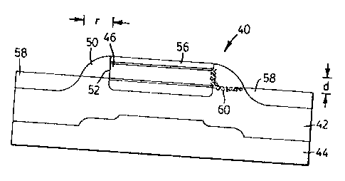
junction of a silicided single polysilicon bipolar transistor 40 (Fig. 3) is
used
as an antifuse. As will be discussed, this arrangement allows the distance
between the metals on the base and emitter regions to be reduced by
approximately a factor of five, and this distance is better controlled since
it
is defined by self aligned processing steps. The shorter distance between
the base and emitter metals in the silicided single polysilicon bipolar
transistor 40 serves to lower the applied voltage and energy required to
switch the antifuse from its OFF state to its ON state by a factor of
approximately two, as compared to a planar diffused bipolar transistor. As
mentioned, the lower programming voltage is a substantial advantage,
because in the process of programming the antifuse, the surrounding
circuitry is much less likely to be damaged.
In a preferred embodiment, the transistor 40 is constructed as
follows. Firstly, the base region 42 (shown as a P-type region but the types
can be reversed) is implanted into an n-epitaxial or n-well region 44 of
monosilicon. Next, n-type polysilicon is deposited and patterned on top of
the base region 42 to form the emitter 46. These steps are, as usual,
-6-
lithographic steps.
Next, a layer of silicon dioxide (not shown) is deposited by
chemical vapor deposition and is then subjected to anisotropic plasma
etching, resulting in a ring-shaped sidewall oxide spacer 50 encircling the
sidewall 52 of the emitter 46. It is a well known feature of anisotropic
etching of an oxide layer (as shown by U.S. patent 5,019,878) that the
thinner portions of the oxide layer are removed during the etching
process, but that an oxide ring remains from the thicker portion where a
feature projects above the surrounding surface. The radial dimensions of
the sidewall ring 50 (as shown by dimension "r" in Fig. 3) are well defined
by the process step and are not defined by a lithographic step.
Next, the exposed emitter polysilicon 46, and the base silicon
42 (which as mentioned is monocrystalline silicon) are silicided by
depositing one of the following metals at elevated temperature: Co, Mo,
Ni, Pt, Ta, Ti or W (Pt is shown as an example). Such siliciding is well
known in the art. At elevated temperatures, these metals react with all
exposed silicon to form a silicide, but they do not react with the silicon
dioxide layer or sidewall ring 50. Consequently, etchants can be used to
remove the unreacted metal and leave the silicide in place. By this
process, the transistor 40 shown in Fig. 3 is fabricated.
As shown, the transistor 40 in Fig. 3 now has a low resistivity
contact (e.g. of platinum silicide) 56 on the emitter 46, and a surrounding
low resistivity contact layer 58 (e.g. of platinum silicide) on the base 42,
with only a short distance between these two contacts, defined by the oxide
ring or sidewall spacer 50.
When a controlled programming voltage is applied between
the contacts 56, 58, electrical and then thermal breakdown occur between
the base 42 and the emitter 46, causing a silicide filament 60 (e.g. platinum
silicide) to grow. Typically the height or dimension "d" of the sidewall
oxide spacer 50 is about 0.4 microns, and its thickness in the radial
dimension "r" is about 0.25 microns, so the total length of the filament 60
is about 0.65 microns, while its width is typically about 0.35 microns. This
21.9~62'~
-7-
length (0.65 microns) is far less than the length of the filament required in
a conventional bipolar transistor, and therefore requires less energy to
produce.
A simple circuit used to program antifuses of the invention is
shown in Fig. 4. As shown, firstly a measuring instrument 64 is connected
to transistor 40 (drawn for convenience as a zener diode) to measure the
emitter-base breakdown voltage of transistor 40. Next, a voltage pulse was
applied from voltage supply 66 through a 250 ohm current limiting
resistor 68 to the emitter-base junction. In the specific transistors 40 used,
it was found that the breakdown voltage was approximately 5 volts (this
varied slightly from device to device), and that a voltage pulse of 9 volts
superimposed on the breakdown voltage (total approximately 14 volts)
was optimum for producing the filament 60.
Fig. 5A shows a plot of the voltage pulse versus time used to
form the antifuse (i.e. the filament 60). The top trace 70 shows the pulse
applied by the voltage source 66 at terminal A of the current limiting
resistor 68. The bottom trace 72 shows the voltage at the input terminal 58
of the device, namely the emitter-base voltage. The voltage pulse was of
about 5 milliseconds duration, with a rise time (shown by curve portion
74) of approximately 150 microseconds. It will be seen from the portion 74
of plots 70, 72 that the entire antifuse process (the formation of the
filament 60) occurs within the short rise time of the pulse 70.
Fig. 5B shows the same pulse applied to the device 40 after
formation of the antifuse. The top trace 78 shows the voltage pulse
applied to the top terminal A, while the lower trace 80 shows the voltage
pulse applied to the emitter 58, i.e. the emitter-base voltage. It will be
seen
that no further changes to the junction are observed from this pulse, i.e.
the filament 60 has already been formed and no further filaments are
formed.
Fig. 6 displays a curve 82 showing the emitter-base breakdown
voltage distribution for a number of functional discrete transistors 40
before the filament forming voltage pulse 74 was applied. It will be seen
~~~6~7
_8_
that the mean emitter-base breakdown voltage was approximately 5 volts,
but that there was (as would be expected) a fairly substantial variation from
this level. The voltage pulse applied was, as mentioned, 9 volts plus the
measured emitter-base breakdown voltage.
After formation of the filaments 60 on a number of devices
40, voltage measurements of the collector/emitter-base junctions were
made at bias current levels of 50, 100, 150 and 200 microamperes, and
impedances were calculated. Fig. 7 shows the data for the impedances at a
50 microampere bias current with the number of devices plotted on the
vertical axis and the impedance on the horizontal axis. Curve 84 plots the
average of the impedances found. The mean impedance was
approximately 73 ohms with a standard deviation of 16 ohms. This was a
relatively low impedance, bearing in mind that the impedance before
formation of the filament 60 was nearly that of an open circuit.
Fig. 8 shows the entire population of the sample shown in
Fig. 7. The number of devices appears on the vertical axis and the
impedance on the horizontal axis. It will be seen that there are three
outlying devices 90, 92 and 94 between 600 and 800 ohms. This indicates
that a small percentage of the devices subjected to the filament forming
voltage pulse will exhibit a partial antifuse characteristic. This appeared to
indicate process flaws or structural differences in the transistors in
question and is indicative of some yield loss during production, in the
samples tested.
Fig. 9 plots at 100 the mean impedance (on the vertical axis) at
each bias current (on the horizontal axis) for typical devices after the
antifuse filament 60 was formed. It will be seen that the impedance drops
from 72.9 ohms at 50 microamps bias current to 70.9 ohms at 200
microampere bias current. This relatively small variation does not cause
difficulty in use.
With the devices tested, it was found that pulses of less than
12 volts total (reverse breakdown voltage of 5 volts plus a 7 volt pulse
superimposed) were not sufficient to create the antifuse filament, while
~~~~s~~
-9-
pulses greater than about 15 volts total (5 volts breakdown voltage plus 10
volts superimposed) tended to create junctions having much higher
resistances (more than 300 ohms and increasing with voltage). As
mentioned, pulses of approximately 14 volts (9 volts plus the breakdown
voltage) were ideal.
It was also found that the average energy during the rise time
part of the pulse, where the filament was actively formed, was
approximately 6.6 microjoules. Thus, it will be seen that only a relatively
small amount of energy is needed to program the devices.
In some tests, a rise time of less than one-tenth the rise time
disclosed (approximately 12 microseconds instead of 150 microseconds)
was used, and the antifuses produced tended to have higher impedances
and a broader distribution of impedances. It is not known at the present
time whether the longer rise time of the voltage pulses used was beneficial
in forming the antifuse filaments 60, but it is suspected that the relatively
slow rise time may have been beneficial since it allowed the filaments 60
an optimal time to form.
While preferred embodiments of the invention have been
described, it will be realized that various changes may be made within the
scope of the invention. For example a variety of semiconductors and
metals can be used beyond those specified, and the region specified as p
and n can take on the opposite type if desired.