Note: Descriptions are shown in the official language in which they were submitted.
2198162
TITLE: ANTENNA-EI;FECT SUPPRESSOR METHOD
AND DEVICE PAI~TICULARLY li'OR
THERMOCOUPLES AND OTHER DISSIMILAR METAL
CONDUCTOR COMBINATIONS
BACKGROUND OF THE INVENTION
1. FIELD OF TI~E INVENTION
Tllis inventioll relates generally to electrical devices SUCIl as
multi-part pl~lg and socket assemblies, switches, feed
througlls, test leads, signal wires, and relays, and more
specifically relates to electrical devices that incorporate an
antenna-effect inllibiting feature to protect signals carried by
tlle device from electromagnetic and/or electrostatic
discllarge type interference.
Tlle invention relates fllrther to protecting electrical circuits
from receiving electromagnetiG or electrostatic discllarge
interference wllicll migllt be indllced in condllctors leading to
tlle electrical circuit. More specifically tlle invelltion relates
to electrical conllectors wllicll provide for sllppression of
e!ectromagnetic or electrostatic discharge interference by
means wllicll folln part of tlle conlleclor itself or as an
accessory tllereto.
~ 2198162
This invention applies to the fields of use wherein there is
necessity for including an electrical device in a low level
signal circuit, e.g. a thermocouple sensor, and provides a
new apparatus for eliminating undesired electromagnetically-
induced or electrostatic discharge type stray signals.
2. DESCRlPTlON OF THE PRIOR ART
In the prior art of connectors there are disclosures of the use
of ferrite material in the following:
(I) U.S Patents assigned to AMP Inc: 4,699,590, 4,359,620,
3,789,263, Re29,258, 3,735,705, 3,987,380, 4,936,800.
(II) U.S Patent assigned to The Wbitaker Corp: 5,219,305.
(III)U.S Patent Wiltiam Baird Fritz 3,743,978
(IV) U.S Patent assigned to Stanford Researcll Institllte and
Amplex Corporation: 3,533,948.
(V) Un-examined Japanese Patent Application, AMP Inc.,
90-032246/05 JO 1279-584-A discloses an electrical
connector whicl1 has a noise filter witll a ferrite head fitted to
a terminal lead formed by a central conductor of a feed-
through capacitor.
(VI) German Patent assigned to AMP Inc., Auslegescllrift
No. 2,058,419 discloses a method for the manufacture of a
higll frequency filter from a ferrite tube, wl1ich is in the form
of a highly compressed tube and wl1ich is bonded on its outer
surface with a covering of dielectric material, the layer of
dielectric material carrying an electrode in tlle form of a
metallic outer sleeve, and a further electrode is provided in
similar manner on tlle inside of tlle ferrite tube, characterised-
in tl~at tlle covering (6~ of dielectric material is laid down - '
~ 2~9~162
directly onto the outer surface of tlle ferrite tube (5) by
electrophoresis.
SUMMARY OF THE INVENTION
It is known that electrical signals carried by connectors, or
adjacent apparatus, may be subject to electromagnetic
interference as the result of induced signals picked up from
the radiation of adjacent electrical equipment. Such
interference results from leads acting as an antenna that
senses stray electromagnetic radiation; accordingly, the
sensing of stray signals in tllis manner is known as the
"Antenna-effect". Various efforts have been made to avoid
or suppress the result of the antenna-effect, but such efforts
have been found to be inconvenient and/or expensive to
implement, or botll.
For example, it has been found in tlle past that antenna-effect
stray signals can be avoided by encapsulating leads in
sheaths of magnetic-sllielding sheet material, or by
determining the strength of nearby stray signal fields and
then moving all such nearby sources to a physical distance
from the leads that has been calculated to prevent tlle
possibility of undesired signals being picked up by
electromagnetic induction. It can be seen, readily, that such
preventive methods and tecllniques are indeed costly and
inconvenient. Other attempts to reduce or avoid antenna-
effect stray signals have involved the use of ferrite cores.
However, until now such uses have required additional circuit
elements, such as insertion of a jumper cable, having a
permanently included ferrite core, in series with the main
conductors in the circuit; or, awkwardly and inconveniently
surroundin~ one or more of the circuit conductors with
separately applied ferrite cores.
2198162
It is established practice, in industries that make use of
thermocouple sensors, to couple the sensor into a related
electrical circuit by means of an electrical connector. Wllen
for example tllermocouples are connected to instruments SUCII
as panel meters, controllers and transmitters, the input signal
from the sensor or transducer usually travels substantial
distances along fine gauge electrically conductive wire leads.
The length and nature of such leads and the environment in
which the~ must function often create conditions tllat favour
occurrence of the antenna-effect. In many cases, tlle leads or
signal wires from a sensor or thermocouple are first attaclled,
for convenience, to an electrical connector, for coupling to
an instrument or tlle like. As soon as tlle conductors of the
connector are electrically coupled to the circuit, a potential
antenna is created. Of particular importance are
thermocouple connectors wllicll are particularly susceptible
to tlle antenna-effect because of the long lead conductive
path of the conductors themselves and the higll input
impedance of tlle instrumentation.
The term ;ferrite", as commonly understood in the
electronics field, denotes a particulate material llaving one or
more oxides of iron in particulate form in a carrier such as a
plastics material. Tllis usage of the term "ferrite" is to be
distinguished from tlle usual dictionary definition whicll is a
generic name for a number of oxides of iron. ln this
specification, tlle term "ferrite" is to be understood as
including ~7ithin its scope any suitable material llaving an
absorption and/or shielding effect as concerns
electroma~netic waves wllicll may be emitted at or adjacent
to a zone of completion of an electrical circuit. Kno~vn
ferrite elements consist of ferrite material sintered into a
convenient shape. Other known "ferrite" materials for the
suppression of electromagnetic interference are nickel-zinc
compositions and manL~anese-zillc materials, of different
compositions to permit selection of an optimum type for a
2i98162
given application; pressed parts, components, and powders
are known.
OBJECTS OF THE INVENTION
Accordingly, it is an object of tllis invention to provide
means associated with an electrical device tllat is capable of
avoiding stray signals that may be induced in the leads of the
device .
It is another object of this invention to provide an apparatus
for eliminating the effects of undesired stray signals in
circuits, tl~at is uncomplicated in design, and that is simple
and relatively inexpensive to produce.
It is stil~ anotller object of tllis invention to provide mealls
associated with an electrical device for eliminatill,s~ tlle
effects of undesired stray signals in its circuits, tllat is easily
adaptable to single-wire or multi-wire connections.
Anotller and further object of tllis invention is to provide
means associated with an electrical device for eliminating the
effects of undesired stray signals in its circuits, tllat can be
manufactured easily in various configurations to
accommodate differing circuit requirements.
And yet anotller and furtller object of tllis invention is to
provide means associated with an electrical device for
elimination of the effects of undesired stray signals in its
cjrcuits in wllicll operative elements of the device may be
configllred to facilitate insertion and rellloval of wire
conductors .
2198162
A further object is to provide a method for the formation of a
twin, or other multiple, wire arrangement, such as a
thermocouple, assembly with a housing composed wholly or
mainly of ferrite material, for example by molding or
machining.
A further object is to provide a single wire arrangement, e.g.
for a "banana" type plug and a method of incorporating the
single wire in a housing composed wholly or mainly of ferrite
material, for example by molding or machining.
Other objects are to provide:-
(A) In an electrical device e.g. a plug and socket, a switch ora relay, whicll includes at least two contact members with
respective surfaces, for bringing into contact to establish an
electrical connection, antenna-effect inhibiting means
disposed adjacent to the connection surface of at least one
said contact member.
(B) An electrical device wherein said ar,tenna-effect
inhibiting means is a ferrite element, as defined herein.
(C) An electrical device wherein said at least one contact
member is one part of a multi-part plug and socket connector.
(D) An electrical device wherein said antenna-effect
inhibiting means is incorporated as a structural element of
said device.
(E) An electrical device wherein said antenna-effect
inhibiting means is a module separably incorporated with said
device, or attachable thereon.
(F) An electrical device wllerein said antenna-effect
inhibiting means surrounds said connection surface, and
2~99162
particularly may be a multi-part element assemblable about
said connection surface.
(G) An electrical device wherein said antenna-effect
inhibiting means is incorporated in said one contact member,
or forms a housing for said at least one contact member (e.g.
by forming the housing from ferrite).
(H) A method of making a connector, for at least one metal
element, having a connector shell of ferrite material about
said element or elements, made for example by molding or
machining.
(I) A further object is to provide a connector, for one or a
plurality of wires, wllerein the or each wire is connected to a
terminal via a signal actuated means, for example, a signal
modifying means and/or a signal indicating means, and
wherein the signal actuated means and its connections to the
or each wire and to the or each terminal are housed ~vholly
within a ferrite body.
DESCRIPTION OF THE PREFERRED EMBODI~IENTS
In one form of this invention the electrical device includes
two or more discrete contact members witll respective
surfaces for bringing into contact to establish an electrical
connection, and llas respective antenna-effect inhibiting
means disposed adjacent to the respective connection surface
of each said contact member.
A feature of this invention is the provision for association
with an electrical device of a signal inhibiting ferrite element
that surrounds a wire lead intended for connection in a
circuit, so as to prevent the propagation of stray signals
through the device to undesired parts of the circuit.
219~1~2
lt has been found that ferrite elements, when properly
included in an electrical circuit, act as an electromagnetic
"sponge" to absorb the unwanted electromagnetic wave
energy and to reduce or eliminate the antenna-effect of the
conductors with which the ferrite elements are associated.
Ferrite connector housing shells may be formed by molding or
machining ferrite compositions.
Further, a method of making a connector, for two wires of
dissimilar metals, comprises forming a connector shell of
ferrite material embracing both of said wires.
Further in accordance with the invention, a metllod of 1naking
a connector, comprises forming a connector shell of ferrite
material about a metal element.
Still further, a method of making a connector, for at least one
metal element, comprises molding a connector shell of ferrite
material about said at least one metal element.
In another method of making a connector, for at least one
metal element, there is provided ferrite material which
embraces said at least one metal element, and whicll is
machined to shape.
The invention further provides a connector, having at least
one metal element therein, comprising a body of ferrite
material molded about said at least 01le metal element.
The invention still further provides a connector, having at
least one metal element therein, with ferrite material
embracing said at least one metal element and machined to
shape.
BRIEF DESCRIPTION OF THE DRAWINGS
- 2 1 9
These and other and further objects, features and advantages
of tllis invention will be made apparent to tllose having skill
in this art, by the following specification considered with
reference to the accompanying drawings, in which:
Figure 1 is a partially cut-away pictorial representation of
one embodiment of an electrical device module and ferrite
element in accordance with this invention;
Figure 2a and 2b are a pictorial representations of two
modified forms of the ferrite element used in the device of
Figure l;
Figure 3a and 3b are a pictorial representations of other
forms of ferrite element that can be used in this invention;
Figure 4 is a plan view of a different form of device
including a ferrite element in accordance with this invention; ,-
Figure 5 is a pictorial representation of an embodiment of an - -
electrical device including a ferrite element in accordance
with this invention, having an integral wire conductor lead;
Figure 6 is a pictorial representation of an embodiment of
this invention including a separable, two-piece electrical
devtce;
Figure 7 is a front elevation view of female portions of a
two-piece device sucll as is shown in Figure 6, shown
mounted in a multiple array in a panel;
Figure 8 is a pictorial representation of another embodiment
of an electrical device including a ferrite element in
accordance with tllis invention, illustrating tbe signal-
inhibiting element mounted to a connector llousing in external
configuration;
~ 2198162
Figure 9 is a plan view of the electrical connector of Figure
7, showing an alternate arrangement for extending a wire lead
from the device;
Figure 10 is a pictorial representation of another embodiment
of an electrical device including a ferrite element in
accordance with this invention, illustrating the signal
inhibitiny element mounted in an external retro-fit
configuratioll on an existing device that did not incorporate a
ferrite element in its original construction;
Figure I l is a pictorial representation of a device including a
ferrite element in accordance with this invention, in the form
of a terminal strip;
Figure 12 is a pictorial representation of a different form of
the terminal strip connector shown in Figure 11.
Figure 13 shows a male plug with split ferrite sleeves on each
pln.
Figure 14 is an elevation of a representative test meter
having a pair of leads in eacll of wllicll there is an antenna-
effect inllibitillg means incorporated at the juncture of the
lead with the meter.
Figure 15 is an elevation of two leads, for use with a test
meter, each llaving a different form of connector to engage
with tertninals of a meter (not shown).
Figure 16 is an elevation of a test meter having, for example,
a thermocouple probe connected to it by a twin-core lead
wllicll is enclosed, at its point of entry to the meter, by an
antellna-effect inllibiting sleeve.
2198~62
Figure 17 is an elevation of a test meter in wllich the twin-
core lead is connected by a two-pin plug incorporating an
antenna-effect inhibiting sleeve.
Figure 18 is an elevation of a test probe, with twin core lead,
wherein an antenna-effect inhibiting member, such as a
sleeve or a collar, is provided both where an elongated probe
joins a llandle, and wllere a two-core lead jOillS a two pin
plug.
Figure 19 is a partial elevation of a tWO-pill plug having
incorporated tllerein a so called wire caddy wllich includes a
sleeve of antenna-effect inhibiting material.
Figure 20 is a perspective view of a completely assembled
plug, of tlle kind showll in figure 19, showing how the twin
lead to tlle plug passes from tlle plug through the s}eeve and
is then stored temporarily by wrapping about tlle wire caddy.
Figure 21 is a partially sectioned view of a two-pin plug to
sllow both an internal collar, and an external sleeve, adapted
to surround the wire leads to its terminal pins.
Figure 22 is an axial section of a banana plug adaptor
including a sleeve of antenna-effect inhibiting means.
Figure 23 is a partially sectioned view of a two-pin adaptor
wherein eacll pin-and-socket assembly has a collar of
antenna-effect inhibiting material about tlle pin portion of the
assembly.
Figure 24 is a partially-sectioned view of a two-pin plug
assembly having a collar of antenna-effect inhibiting material
about the entry for the leads, and also a furtller such collar
about eacll pin.
11
2198162
Figure 25 is a partially-sectioned view of a single -conductor
lead having at one end a crocodile clip, and at the other end
a banana plug.
Figure 26 shows, with the components thereof in separated
condition, a first form of two-pin male connector having a
body structure of ferrite material.
Figure 27 shows, with the components thereof in separated
condition, a second form of two-pin male connector having a
body structure of ferrite material.
Figure 28 shows, with the components thereof in separated
condition, a third form of two-pin male collnector having a
body structure of ferrite material.
Figure 29 shows, witll tbe components thereof in separated
condition, a first form of two-socket female connector having
a body structure of ferrite material.
Figure 30 shows, witll the components thereof in separated
condition, a second form of two-socket female connector
having a body structure of ferrite material.
Figure 31 is a perspective view of the connector of figure 26,
when fully assembled, and sllowillg an additional coating
material having identification marking thereon.
Figure 32 is a perspective view of a connector, fully
assembled, corresponding substantially to that of figure 26,
and showing an additional protective sheath about the body.
Figure 33 is a perspective view of a modification of figure
27, to show a window for access to the interior of the
connector.
- 12
t ~ ' ~
2198162
Figure 34 is an elevation of a pair of identical single-wire
leads, e.g. wires of a pair of dissimilar metals, each of which
has at one end, adjacent to a banana plug, a sheath in the
form of a cylindrical plug body or casing of ferrite material.
Figure 35 is a perspective elevation of a further form of
connector, for a thermocouple pair, which includes a signal
indicating and/or modification means disposed, with its
connections, wholly witllin a ferrite body.
Figure 36 is an elevation of a component utilising a ferrite
core for the protection of a telephone line.
Figure 37 is a perspective elevation of part of a printed
circuit board whicll incorporates a ferrite protected
connector.
Figure 38 is a perspective elevation of an electronic
component, incorporating solid state circuitry, wllerein a case
for tlle component is made of ferrite material.
DETAILED DESCRIPTION OF T~IE INVENTION
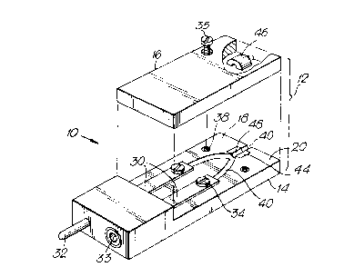
Referring now more specifically to the drawing, Figure I
may be seen to illustrate a device including a ferrite element
in accordance with this invention in whicll the connector
device 10 comprises a housing 12 of insulating (e.g. ferrite
composition) material having a first separable housing
portion 14 and a second separable housing portion 16 that are
configured to engage each other about a common separation
plane 18 that extends in substantially parallel, co-planar
relationship with a contact-element supporting face 20 on
first housing portion 14. A pair of contact elements 30 are
mounted on the housing, althougll it is considered obvious
that just one or substantially more tllan two contact elements
may be mounted to tlle llousillg if desired. Similarly,
13
~ 2i98162
although the contact elements 30 shown in Figure 1 are of the
type commonly identified as male contact elements, it is
considered obvious that other types of contact elements, such
as the female contacts shown and described elsewhere in this
specification, may be used in lieu of the male contacts,
without departing from the spirit and scope of this invention.
In Figure 1, one of contact elements 30 includes near one end
a male end portion 32, and the other contact element includes
near a corresponding end, a female contact receptacle portion
33. Botl1 the male and female contact portions 32 and 33 are
adapted electrically and mechanically to engage a mating
external conductor (not shown) in any obvious and ~vell-
known manner, in tllis case, it is apparent that tlle mating
external conductors would be a mating female contact
element for male contact portion 32 and a male contact
element for female contact portion 33. External conductors
having these conventional shapes, will electrically and
mechanically engage male contact portion 32 and female
contact portion 33 in a manner well known to those having
skill in the electrical connector art.
Each electrical contact element 30 further includes, at the
opposite end remote from the male and female contact
portions shown, a screw terminal 34 for electrically coupling
the contact 30 to a second external conductor (not shown).
For this purpose, the second external conductor may have any
suitable form, such as flexible insulated electrical wire, that
is suitable for coupling to, i.e. electrically and mechanically
engaging, screw terminal 34, so as to establish an electrical
path extending through and away from connector 10, via
contact 30 and the external conductor. Contact 30, and any
external conductors to which it is coupled, together form an
electrical path extending through and away from the housing
12.
The two separable portions 14 and 16 of housillg 12 are
secured to~ether by any convenient fasteoing means, such as
14
~ 2198162
one or more fastening screws 35 and mating threaded bores
38. Portions 14 and 16 preferably are secured together after
screw terminals 34 have engaged one or more external
conductors to contact element or elements 30, so as to
provide a cover for each screw terminal connection and to
form a unified conneclor housing 12.
Housin~ portion 14 includes a conductor guide groove 40 that
serves to constrain and to guide an external conductor from
screw terminal 34, out of and away from l~ousil1g 12. Along
the portion of the path represented by tl1e groove 40, a first
part 44 o~ a toroidal ferrite core element 42 (shown in figure
2) is secured to holding portion 14, as by gluil-g, force-
fitting, molding or any other suitable means, into the
electrically insulating material of the housing. The second
part 46 of ferrite core elemel1t 42 is secured to housing
portion 16 in any similarly convel1ient manner, in pOSitiOt1 to
mate with first part 44 so as to form a complete toroidal
structure, having a conductor passage 48 extending there
througl1 as shown in Figure 2, when housing portions 14 and
16 are fastened togetller as by fastening screws 35.
The ferrite core members 42 illustrated in Figure 2a and 21
are intended to illustrate tlle characleristic toroidal and
cylindrical shape of sucl1 cores. In this particular
embodiment, the core 42 or 42a is divided into two l1alves,
44,46 or 44a,46a which together form respectively a complete
toroid or cylinder shape. The end faces 50,52 and 5~,56 of
the core halves 44,46 may be provided, as showll in Figure
2a, witl1 mating projections 58, and receptacles 60, to help
align and maintain the relative positions of the two l1alves
when they are brought together in mating relationship. The
division of core 42 into two halves 44,46 accommodates the
particular design and uses of the connector illustrated in
F.igure 1, but it should be understood that other ferrite
element confi~urations can l)e used in conllectors constructed
in accordance witl1 this invention, inclllding unitary one-
2198~62
piece elements as illustrated respectively in figures 3a and3b. A conductor passage here shown as passage 48, is to
accommodate a portion of the axial lengtll of a conductive
path along which electrical signals will be transmitted.
In the connector device embodiment illustrated in Figure 3b,
the axial length dimension X, of the ferrite element 42', is
shown to be comparatively short relative to the diameter of
the conductor passage 48. It should be recognised, llowever
that dimension X may be increased by any desired amount, so
that the shape of element 42 or 42' may eventllally more
nearly represent a tube as in figure 3a, rather that1 a
doughnut-shaped torus. For the purpose and uses of this
invention, both tubular and toroidal sllapes may be used, and
either shape may be eitller unitary as sllown in Figures 3a and
3b, or divided into separable sections as suggested in Figures
2a and 2b.
Although the terms "toroid" and "cylindrical'~ have been used
in this description with reference to figures 2a and ~b and 3a
and 3b it will be understood that other enclosing bodies may
be used having a regular or irregular curved or pol~ ~onal
cross- section, and that tlle nature of the cross-section may
change along the lengtll of the enclosing body.
Figure 4 illustrates, for purpose of completeness, an
electrical connector device assembly having a pair of male
contact members 132 extending from a two piece housing 114
in which a unitary ferrite element 142, of the type illustrated
in Figure 3a or 3b, is enclosed when the two parts of the
housing are brought together and secured by one or more
fasteners such as screw 138, in the manner described above
with reference to the connector of Figure 1. In tllis
connector, one or more external conductors such as ~ire
leads may be separably fastened to the ends of contact
members 132 within the llousing in tlle same or any similar
manner described with reference to the conllector in l~igure l,
16
2 ! 98 1 62
so that such external conductors may be passed through the
conductor passage 148 of element 142 and extended
outwardly from housing 114 via an exit passage 62
corresponding generally to exit passage 40 of Figure 1.
Figure 5 illustrates an electrical connector device 70
including a ferrite element in accordance with this invention
pre-assembled to a tllermocouple 72 by means of a pair of
elongated wire leads 74 that may be made, typically, from
dissimilar metal. It is known that dissimilar conductive leads
in this configuration will heighten the antenna-effect pickup
of stray electromagnetic signals. A connector permanently
attached to the ends of such leads remote from the
thermocouple device, accordingly will be found to be
especially effective in eliminating the effects caused by such
stray signals.
In this embodiment of the invention, the housing 214 supports
a pair of electrical contact members llaving male contact
portions 232 extending from the housing. Wire leads 74 are
coupled to the electrical contacts of male portions 232 within
the housing 214, and they extend outwardly from tlle housing
after passing througll an embedded ferrite elemenl 242 within
the housing. As explained previously in connection with the
embodiment of the invention illustrated in Figure 1, any
number of associated conductors such as wire leads may be
made to pass outwardly away from the housing tllrough an
appropriately-sized internally-positioned element 242.
Figure 6 illustrates a two-part mating electrical connector
device assembly 310 having a female half 313 and a male half
315, each having one or more wire leads 374 extending
outwardly and away from their respective housing members
317 and 319. Female connector portion 313 includes a pair
of electrical contacts having female receptacle portions 333
mounted to the housing and male connector portions 3l5
includes a pair of electrical contacts having male contact
17
2198162
portions 332. The contacts may be mounted to the housing in
any known manner as previously described, and wire leads or
otller suitable forms of external conductors may l~e
electrically coupled to the electrical contacts within the
housing, also in any known manner. In connector housing
half 313 the tubular-shaped female receptacle portions 333
are each surrounded by ferrite elements 342 which may be
either toroidal or tubular in shape. The elements 342 are
made to surround the female portions 33 by extending their
tubular bodies through a conductor passage 348 in each
element 342. It can be seen readily that this structure
affords the advantage of immediately and effectively
surrounding an axial portion of the length of the continuous
electrical flow path that is formed when the male contact
portions 332 are mated with the female contacts 333 in
accordance with customary electrical connector usage.
ln Figure 7, a plurality of female connector devices 413
which may be similar or identical to connector halves 313
shown in figure 6, are mounted in substantially parallel, side-
by-side array in a panel member 411. In the manner of tlle
connector halves 313 shown in Figure 6, each unit 413
includes a pair (or any desired number ) of female contact
portions 433, each surrounded by a ferrite element 442
having a central passage 448. This figure is intended to
illustrate how a connector in accordance with this invention
may be mounted for convenient use in multiple array.
Suitable conductive leads may be internally connected to
contact portions 433 and allowed to extend outwardly away
from cotinectors 313 in a rearward direction. For the purpose
of clarity it is noted that the rearward direction extends
beneath the plane of this drawing and the wire conductors,
therefore, are not shown. When the connectors 413 are
mounted in this manner in a supporting panel 411, they may
be used readily and conveniently to couple with any suitable
form of external conductor that can be inserted and/or
18
2198162
witlldrawn from tl1e axial central openings XX witllin female
contact portions 433.
In the embodiment of this invention illustrated in Figure 8, a
connector device S10 having a housing 512, with first and
second separable portions 514 and 516, and a pair of male
contact members 532 mounted thereto, further includes an
externally mounted ferrite element 525 supported on the
exterior of l1ousing 512 by means of a support bracket 543
coupled to housing portion 514. It will be understood,
however, that bracket 543 can be mounted readily to either
housing half 514 or 516, within the scope of the invention.
The bracket 543 may be made of metal or plastic, although
plastic is preferable to preserve the conductive symmetry of
the element so as to optimise the capture of stray
electromagnetic signals.
Figure 9 illustrates tlle connector of Figure 8 in whicl1
external conductors 574 in the form of lead wires extending
away from the connector housing 514 have been looped
tl1rough the e~cternally mounted element 525 so that tl1ey pass
through the conductor passage 548 in the element at least
twice instead of merely once. It has been determined that
this looped configuration can provide enhanced antenna-
effect signal absorption when desired.
Figure lO illustrates an alternate form of constrllction for tlle
conl1ector device of Figllres 8 and 9, in whicll an externally
mounted element 648 is supported by a bracket 643 that is
separately attaclled to the exterior of the connector housing
612. The means of attachment may be known separable
mounting means such as, for example, a pair of screws 638,
that are threadedly engaged to threaded bores 38 first
described herein with reference to Figure 1. ln this regard, it
sl1ould be noted that a bracket 643 with an element 648 may
be mounted, if desired, to the connector housing illustrated in
Figure 1, using the same fastening screws 35 (as shown in
19
2~98162
figllre 1) to secure tlle bracket to tlle housing and to secure
togetller tlle separable llousing parts 14 and 16.
Figures 11 and 12 illustrate embodiments in accordance witl
this invention in tlle form commonly identified in the
electrical conllector indllstry as terminal strips. The terminal
strip connector 710 of Figure I 1 comprises a housin~ 712 of
insulating material llaving a plurality of parallel spaced-apart
barrier ~valls 780 extending from a contact supporting surface
720 on one side of the strip. In each space 782 bet- een
adjacent barrier walls 780, a metallic contact XX of
generally knowll design and fullctioll is moullted Oll or in
surface 720, in wllole or in part. Each sucll contact XX may
llave for example, a screw termillal 734 tllreadedly engaged
to tlle conductive material of tlle contact for separately
SeCUrillg all eXterllal COlldllCtOr, SIICIl as a wire lead,
electrically and mechanically to tlle strip; whell a separate
wire lead is connected to tlle screw termillals at each end of a
contact strip XX, a continllolls electrical patll is establislled
from one e~terllal conductor to tlle otller tllrougll lhe contact
strip XX and e~ctendillg outwardly and away from tlle terminal
strip in two directions. It will be ullderstood, of course, tllat
electricity will be assumed to flow, accordin~ to conventioll,
primarily in one direction tllrougll the patll tllus establislled.
In accordance witll tllis invelltioll, in eacll space 78~, an
element 742 llaving a condllctor passage 748 is mounted to
tlle bod~ 712 of terminal strip conllector 710, so tllat the
correspondill~ contact strip XX extends tllrou~ll tlle
condllctor passage 748 witll tlle screw terminal portions 734
at opposite ends of tlle contact XX beillg positioned Oll
axially opposite sides of the ferrite elemellt 742. In this
manller it will be ullderstood readily by those having skill in
tllis art, tllat the COlltillllOIIS electrical patll extendin~ thollgl
the contacl elemellt XX will also extelld ll)rougll a ferrite
element 742, thus providin~ an improved ternlinal connector
strip in wllicll eacll conllected wire lead will benefit from tlle
antelllla-effec~ suppressioll of the core witllout requirillg any.
2198162
additional structure or additional serially connected wire
leads.
Figure 12 illustrates a modified form of a terminal strip
connector device 8~0, in wllich tlle llousing member ~12
further includes a separable cover portion 814 tllat is
configured to be separably retained between pairs of
adjacent, spaced-apart barrier walls 880 itl any convenient
manner, sucll as interference fit or inter-engaging projections
and retention shoulders (not showll) of well-known design. A
ferrite element divided into two parts 844 and 846 is
positioned witll part of the element in tlle hOIISillg body 812
and the other part in tlle cover member 814, sucll that when
tlle cover is engaged to tlle llousing, the elemellt parts 844,
846 will come togetller in alignment to form a complete
element surrounding a corresponding contact elemellt 830.
This configuration may be particularly advantageolls whell it
is necessary and desirable to provide enlarged (in diameter or
in lengtll Ot both) elements to surro~ d paths tllat may be
especially susceptible to stray electromaglletic si~nals of an
ndesired natllre.
In Figure t3 tlle half casing 910 is recessed as at 911, 912
and 913 to receive and locate male pillS 91~ alld 91~, each of
whicll llas an intermediale portion along its lengtll made of
reduced diameter so as to receive and loc~te a respective
ferrite sleeve 916, 917 wllicll is spli~ longit~ldillally
Referring to Figure 14 tllere is SllOWII a representative test
meter 1001 having associated with it lwo test probes 1002
connected by respective leads 1003 to fixed or removable
connectors 1004. Antenna-effect inhibiting collars or
sleeves, for example as described above witll reference to
any of the preceding figures, are enclosed witllill the probes
and/or the conllectols, and encircle tlle cond~lctors thereill.
21
2198162
Referring to Figure 15 tllere are sl1owl1 two conductor leads
1005 and 1010. Lead 1005 llas at one end a llandle 1006 witl
probe 1007, and at the otller end a first kind of plug or
socket connector 1008 on wl1icll is included an antenna-effect
inllibiting collar 1009. Lead 1010 has at one end a handle
1011 witll probe 1012, and at the otl1er end a different form
of plug or socket connector 1013 in wllicl1 tllere is an
antenna-effect inllibiting collar or sleeve (not shown), as
described above witll reference to any of tl1e preceding
figures .
In Figure 16 a meter 1014 receives a collnector 1015, for a
tllermocouple 1016, wllich includes an alltenlla-efrect
inllibiting member (not sllown) whicl1 is of tlle kind referred
to in tlle preceding figures, see especially items 916, 917 of
Figure 13, arranged about botl1 wires.
In Figure 17 a meter 1017 receives a removable connector
1018 for a probe 1019 witll lead 1020. A collar or sleeve, of
antenna-effect inl1ibiting means, as described above, is
disposed witl1 the conl1ector ~018 about at least one of tl1e
conductors tllerein.
In Figure 18, a tl-ermocouple device includes a probe 1021
llaving two conductors (not sllown) wllicll pass tllrougll a
stem 1022 to a conllector plug 1023 removably contlected to a
l1andle 1024 at tl1e end of a tWill lead 1025 termillating in a
two pin plug conl1ector 1026. An antelll1a-effect inl1ibitillg
collar or sleeve, as described precedingly llerein, is disposed
witl1in tl1e conl1ector plug 1023 and about the conductors
therein. Alternatively, or in addition, an antenna-effect
inhibiting collar or sleeve, as described precedingly herein,
is disposed witllin tlle two pin pl~lg conl1ector 1026
Figure 19 and 20 are views of two embodilllellts of two pin
contlector 1027A and 1027B havillg at one end two pins
1028, and at tlle otl1er end a wire caddy 1029. Figllre 20
22
~ 2l98l62 :'
SllOWS a thermocollple 1030 llaving twin leads 1031 wllich are
~~ connected internally of the connector to respective pillS 1028,
and emerge from tl~e connector 1027 to pass througll a sleeve
1032 of antenna-effect inllibiting material. Figure 19 is
partially sectioned to sllow an internal double-radius collar
or sleeve 1033 througll wllicll tlle leads (not shown) would
pass.
Figure 21 shows a two pin connector 1034 whicll receives a
casing 1035 formed with a neck 1036 carrying a head 1037
by whicll the casing 1035 becomes locked lo the conllector
body 1038 when a cover portion 1039 (sllown partially Cllt
away) is fastened in position. Withitl tlle casing 1035 ll~ere
is positioned a sleeve 1040 of antelllla-erfect inllibitillg
material, tllrough whicll passes a tWill conductor 1041.
Referring to Figure 22 there is sllown a "banalla" plug llaving
a metal pin portion 1042 about whicll is positioned a collar
1043 of antenna-effect inllibiting material secured Oll tlle
body 1044 by a sleeve 1045.
Referring to Figure 23 tllere is shown a banana jack adapter
1046 havillg two metal pins 1047 eacll of which is encircled
by a collar 1048 and by a sleeve 1049, both of antentla-effect
inhibiting material, to inhibit such effect respectively where
tlle pins 1047 coact with a socket (not showll) and ~vhere the
sockets 1050 respectively coact with pillS (not shown) of
another componellt.
Referring to Figure 24 tllere is shown, with part broken away,
a two pin connector 1051 having two pillS 1052 each of wllich
is encircled by a respective collar 1053 of antenlla-effect
inhibiting material housed within tlle general body 1054 of
the connector.
In anotller useful arrangemellt a C'm-llti-pl~lg adaptor
comprises a convellielltly shaped body, e.g. a cul)e, llavill~ at
23
2 ~ 6 2
a plurality of its faces respective sets, e.g pairs, of pitlS or
sockets of various sl1apes and dimensions to enable the
adaptor to engage witll plug pins, or sockets, or leads or
other adaptors or devices or components, to enable
connection of otllerwise non-matching items, some or all of
tl1e pins and/or sockets of tlle adaptor having associated
antenna-effect inllibiting means sucl1 as collars, sleeves or
otl1er enclosing or mounting bodies.
In Figure 25 tllere is sl1owl1 a single-conductor lead 1055
having at one end a knowl1 crocodile clip 1056. At tlle other
end there is a banana plug 1057 wl1erein a casing 1058
houses a sleeve I059, of an antenna-effect inl1ibiting
Itlaterial, WlliCIl SllrrOllndS tlle COlllleCtOr (llOt SllO-VIl) ~YIliCll iS
attaclled to tlle plug termil1al 1060. Antenl1a-effect inl1ibitil1g
material, e.g "ferrite", may be present in tlle banalla plug and
in the socket in wllicl1 it is received.
Tlle antenl1a-effect inl1ibitil1g meal1s may be fitted to or
applied Ol1 tlle or eacl1 contact member by methods includil1g
for example pre-forming said means and there after fitting it,
e.g. by snap-fit, use of faslellillgs, or sccurillg ot' portions of
a wllole about tlle contact member, or in anotller manner of
application of tl1e inllibitillg material, e.g. by shril1kil1g in
pOSitiOl1, or spraying it on, or by dipping the contact member
in tlle inl1ibiting material or by enrobing, coalillg, lacquerillg
or spraying.
Tlle quantity, dimensiolls, shaping and otller pllysical features
of the inhibiting means may be selected l)efore application, or
modified after application, for enl1ancement of its effect, e.g.
by tuning to a capacity and/or wavelengtl1 of operation suited
to the kind of antenna-effect interferel1ce to be expected.
Figure 26 sl1ows a conl1ector, for a tllermocollple or a pair of
wires of dissimilar melals, llaving a body of ferrile malerial
witl1 a lower part 2001 and an upper part 2002 wllich can be
24
2198162
assembled by bolts 2003 and nuts 2004. Witllin tlle lower
part 2001 tllere are formed recesses to receive pins 2005 to
which wires 2007 and 2008 can be secured by bolts 2009
witll nuts 2010. Tllermocouples llave an inllerently higll
impedance, rarely less that 8 ohms, usually for long leads.
FigUre 27 Sl10WS a connector, for a thermocouple or a pair of
wires of dissimilar metals, llaving a body of ferrite material
witll a lower part 2011 and upper parts 2012 and 2013, wllicll
can be assembled respectively by a bolt 2014 witll a nllt 2015
and bolts 2016 with nuts 2017. Witllin tlle parts 2011 and
2012 tllere are formed recesses to receive pins 2018tO wllicl
respective wires 2019 and 2020 can be sec~lred by screws
202 1 .
Figure 28 Sl10WS a conllector, for a tllermocouple or a pair of
wires of dissimilar metals, llaving a body of ferrite material
witll a first part 2022 and a second part 2023 wllicll can be
assembled by bolts 2024 witll nuts 2025. Witl~ the part
2022 tllere are formed recesses to receive pillS 2026 to wllicl
wires 2027 can be sccured by l~olts 2028 and IlUtS 2029.
F;gUre 29 Sl10WS a conllector, for a therllloco~lple or a pail of
wires of dissimilar metals, llavin~ a body of ferrite material
with a first part 2030 and a second part 2031 WlliCIl Call be
assembled by bolts 2032 W;tl1 nllts 2033. W;tl1;11tl1e Part
2030 there are formed recesses tO receive female spring
terminals 2034, llaving respective l10US;I1gS 2035, to wllicl
wires 2036 can be secured by bolts 2037 with nllts 2038.
Figure 30 sllows a conllector, for a therlllocouple or a pair of
wires of dis~similar metals, havillg a body of ferrite material
with a first part 2039, and a second part 2040 and a third
part 2041. The part 2040 can be assembled to the part 2039
by bolts 2042 with IllltS 2043, and the part 2041 Cal1 be
assembled to the part 2039 bY a bOlt 2044 W;tl1 a Illll 2045.
Witllin the parts 2039, 2040 al1d 204lll1Cre are fOrmed
2~98t62
recesses to receive female socket terminals 2046 to whicll
respective wires 2047 can be secured by screws 2048. The
terminals 2046 have respective spring clips 2049.
Figure 31 shows a connector, assembled, of the kind
described with reference to figure 26, but with the addition
of a coating 2050 on the ferrite body of a material of, for
example, a plastic, which may serve as a means of protection
against shocks and damage, and/or may carry identification
markings, such as the strips 2051 shown, or dots, figllres or
other marking as desired. The coating may, for example, be
added by dipping or spraying. Marking may be in color or
have'raised tactile indicators, bumps or ridges.
Figure 32 shows a connector, assembled, of the kind
described with reference to figure 26, but with the addition
about the ferrite body of a sheath 2052 for protection and/or
for identification.
Figure 33 shows a connector, assembled, whicll is similar to
that of figure 27, but wherein the two upper body portions
2012-2013 of the ferrite body of figure 27 arc replac ed by a
single upper body portion 2053 assembled to a lower body
portion 2054 by a single screw 205S. In the body portion
2053 there is formed a window 2056, for access to the
interior, wllicll can be left open or can be covered by a cover
portion 2057 wllicll may be detachable (as showll) or may be
hinged to the body portion 2053.
Figure 34 shows an arrangement of"banana" plug single wire
lead which may, of course, be used in twin or otller multiple
sets. On eacll such lead~ a banana plug 2057 llas a collar
secured to one end of a cylindrical block or housing 2059 of
ferrite material through wllicll a single wire 2060 passes
though conventional sleeving 2058 to a spring-loaded
"crocodile" clip 2061. Sucll leads may be used convenielltly-
in pairs to accommodate the dissimilar metal wires of a
26
2198162
tl1ermocouple pair. Where it is desired to terminate a pair of
dissimilar metal wires forming a tllermocouple, the t-vo wires
2060 may be bared at tlle end remote from the banana plug to
provide a tl1ermocouple llead, with omission of the respective
crocodile clips 2061.
It will be apparent to tllose skilled in tlle art that tllere may
be provided one, or again tl1ree, or a greater number, of 1nale
pins, female sockets, connector screws or bolts within tlle
connector bodies of figures 26 to 33, to coact Witll a similar
number of wires. Figures 31 to 34 are preferred
embodimellts, in that tlley SllOW tllermocouples in a ferrite
housing.
It will also be apparent to those skilled in the art that calltion
should be exercised when two physically separated
conductors are carrying a balanced signal. Eacll condllctor
must receive tl1e same protection from tl1e ferrite, otherwise a
common-mode rejection circuit which may be provided in tl1e
instrllmel1tatioll may not be able to compensate for any
unbalance .
Referring to figure 35, there is shown a form of connector
which includes additionally a signal indicating and/or
modification means. Tlle connector has a main body portion
3001 and a removable cover portion 3002 wllicll can be
secured onto tl1e main body portion 3001 in any convenient
manner; for e~cample, by screws 3003 engagillg into tllreaded
lloles 3004. The body 3001-3002 is composed wl1olly or
maillly of ferrite material. Botl~ tl1e maill body portion 3001
and tlle cover portion 3002 may additionally llave a coating,
or sheath, 3005 wl1icl1 may a decorative or protective against
pllysical shocks, or may give an indication of information
concerning tl1e nature of tlle connector or its contents, or any
combination of tllese three functions. ~or example, it may be
a metal sheatll witll stripes, dots, embossing, or figures or
letteri ng
27
~ 2198162
The mai.n body portion 3001 carries two metal tags or pins
3006 for insertion into appropriate receptor sockets of for
example an instrument or a panel.
Within tl1e tnain body portion 3001 there is a recess whicl1
houses a signal indicating and/or modification or modulation
means 3007 having at one of its ends two metal terminals
3008 wl1ich ate attached by screws to tlle int1er end of the
respective tag or pin 3006. At its other end, tlle si~nal
indicating and/or modification or modulatil1g means 3007 has
openings to receive respective wires 3009 of a pair of wires
of dissimilar metals, for e~cample of a thermocouple pair.
These wires are securable in tlle signal indicatil1g and/or
modification or modlllation means 3007 by respecti~e screws
3010. It will be seen tl1at, ~vhel1 ll1e cover portion is secured
in position on the main body portion, the conl1ections
between tl1e wires 3009 and the signal nlodiricatiol1 means
3007, and the conllectiol1s betweell the si~nal indicatil1g
and/or modification meal1s 3007 and the ta~s or pins 3006,
are all entirely or substal1tially entirely conlail1ed ~ i~hil1, and
shielded by, the ferrite material of the connector body.
Whilst the conl1ecfor l1as been showl1 witll two tags or pins
3006, and t~vo wires 3009, it will be apparent to tllose skilled
in tlle conneclor arl tl1at tllree or more sucl1 items may be
used in SUCII a conl1ector.
By way of example, the signal indicating and/or modificatiot1
or modulatiol1 or filtering or amplifying means 3007 may be a
filter, a printed circuit, an etched circuit, a microcl1ip, or
means sucll as a ligl1t for indicatil1g variation of, or passage
of, an electric current, or any combil1atiol1 of these functions.
Clearly, it ~vould be possible to have two or more of the
neans 3007 arranged and conl1ected in series witl1in the
COIllleCtOr, alld differellt SllCIl Inealls 3007 may be applied for
each or son1e of a plurality of wires sucll as 3009.
28
~ 2198~6-2
The means 3007 may be a signal booster for a cable such as
an undersea cable.
Where tlle means 3007 serves to give a visual indicatioll of
modification of or existance of a signal, there may be
provided a small window area, not showll, in tlle body portion
3001, or in the cover portion 3002. Such connector means
may have its means 3007 arranged to be actuated at a
threshold current, and they may be disposed advanta~eously
in a cluster or array witll same or different thresllolds.
To obtain the greatest possible useful effect from tlle
presence of the ferrite material, it is advantageolls if tlle
mating surfaces of any portions of tlle ferrite body shall be as
free as possible from projections or cavities thereill wllich
migllt prejudice tlle acting of the ferrite body electrically as a
single wllole, e.g. it is preferred to make sucll mating
surfaces with a mirror-finish.
l lle rerrite body portiolls or thc Sllell llOll~SillgS 01' the
connectors may advantageollsly be ma(le by macllillitlg or by
molding e.g. in a similar mallller to tlle convelltiollal moldillg
of ceramic bodies. It will be apparent lo tllose skilled in the
electrical conllector arl lllal male plugs, I'clllale ~ockets,
connector t~bs, alld wires, may all be incorporated directly
illtO a molded body at the time of molding of the body,
tllereby to elimillale the need for separable portiolls of tlle
ferrite body, for assembly screws or bolts, and for screws or
bolts for connectioll of tlle wires.
For connectors and other components wllicll are to be used at
higll temperatures, ferrite powder may be mi~ed with ceramic
prior to shaping, formillg etc.
29
219~162
Referring to figure 36 there is sl1own an elevation of a
protective device for a telephone line, e.g. a line entering a
building. The telephone line 4001 has a pair of conductors
4002, 4003 w11icl1 rul1 parallel al1d are 600-ol1m balat1ced.
Tl1e conductor 4001 is wound for several turns about one arm
of a rectanglllar core 4004 of ferrite material. Tlle opposed
arm of tlle core 4004 carries a sl1orted tUI11 4005 of ~ood
condllctor ~vl1icl1 will al~sorb any surges occurril1g.
Referring to figure 37 tllere is SllOWll a perspective elevation
of part of a printed circuit board. Tlle board ~001 has
mounted on it, or secured to it, a cont1ector 5002 ~itl1
terminals 5003. Tl1e connector 5002 is made witl1 a body of
ferrite material.
Referrillg to figure 38 there is sl1owl1 a perspective elevation
of an electronic component incorporating solid state
circuitry. The componel1t 6001 l1as its DIP case 6002 made
of ferrite material from wl1icl1 project contlectors 6003. Tlle
solid state circuitry inside tlle case 6002 is protected by tl1e
ferrite material against interferel1ce from e~ternal
electrolnagnetic or electrostatic interrerel1ce, and lil;ewise
any electromagnetic or electrostatic disturbances wl1icl1 may
originate from tl1e circuitry will be prevented froll1 reacl1ing
adjacent compollellts.
A list (not eYllallstive) of suitable e~an1ples Or pairs of Inetals
for use in tl1ermocollples is:
Copper-constalltall Cllromel-Allllllel
Iron-collstalllall
Cllromel-constalltall Tullgstell-Rllellillm
Platinllln-Platilllllll/Rllodilllll Platil~ulll/Rllodilllll-l'la~illlllll/
R 11 od i u m
2198162
Tungsten-Tungsten/Rllenillm TungstentRllenium-Tungsten
/Rhe11i111n
lt will be seen tllat, in all of tlle constructiolls described
and/or sllowll, tlle connection between tlle wires (of
dissimilar metals) and tlle conllector cond~lctors are fully
sllielded witllin tlle ferrite body.
In connection witll tlle art of printed circuit boardsS it is
furtller proposed tllat sucl- a board may itselr be formed of
ferrite material witll conductive, e.g. copper, circllitry
bonded to tlle ferrite, or again a slleet of ferrite ma~ be
bonded, e.g. cemented, to a printed circuit board after
soldering of the board llas been completed.
Altllougll various specific embodimeMts of tllis invention llave
been described and illustrated llerein, it will be obvious to
tllose havillg skill in tllis art tllat various otller fully
eqUiValellt elllbOdimelltS COllSiStel1t Witll tlle inVClltiOIl are
possible and evidel~t witl~ tl~e scope of this disclosure.