Note: Descriptions are shown in the official language in which they were submitted.
WO 96110298 2 1 9 8 5 q 5 PCr/lJS95/12180
DIGITAL AGC FOR A CDMA RADIOTELEPHONE
5 FIELD OF THE INVENTION:
This invention relates generally to telecommunications
apparatus and, in particular, to radiotelephones that are
compatible with a spread spectrum (SS) code division,
lO multiple access tCDMA) protocol.
BACKGROUND OF THE INVENTION:
A direct-sequence or direct sequence coding spread spectrum
15 communication technique in essence combines two digital
signals, or bit streams, to create a third signal prior to
transmission. The first signal is an information signal,
such as the output of a digitized voice circuit. For
example, the first 5ignal may have a bit rate of lO kb/s.
20 The second signal is generated by a r~n~ . s~quence, or
pseudonoise (PN) generator, and is a stream of essentially
random bits having a bit rate that is several orders of
magnitude greater than the bit rate of the digitized voice
signal. The modulation of these two signals results in the
25 third signal having the same bit rate as the second signal.
However, the third signal also contains the digitized voice
signal. At the receiver, an identical random-sequence
generator produces a random bit stream which mirrors the
original random-sequence that was used for modulation at
30 the transmitter. For proper operation, after oarrier
frequency de-modulation, the PN generator of the receiver
must be synchronized to the i nl i ng PN sequence . By
removing the random sequence from the received signal and
integrating it over a symbol period, a despread signal is
35 obtained. Ideally, the despread signal exactly represents
the original lO kb/s voice signal.
The TIA/EIA Interim Standard, Mobile Station-Base Station
Compatibility Standard for Dual-Mode Wideband Spread
- WO 96/10298 2 1 9 8 5 ~ 5 PCr/US95112180
Spectrum Cellular System, TIA/EIA/IS-95 (July 1993)
specifies in Section 6 . l . 2 that a mobile station shall
provide two independent techniques for output power
adjustment. These two techniques are an open loop
estimation based solely on mobile station operation, and a
closed loop correction that involves both the mobile
station and the cell site controller, or base station. In
the latter technique the mobile station responds to power
control bits received over a Forward Traffic Channel to
adjust its output power level. In the former technique the
received signal strength from the base station is used.
The power control in the CDMA system is also described at
pages lO and 12, and shown generally in Fig. 3-2, in a
publication entitled "Introduction to CDMA and the Proposed
Common Air Interface Specification (CAI) for a Spread
Spectrum Digital Cellular Standard-An Overview of the
Application of Code Division Multiple Access (CDMA) to
Digital Cellular Systems and Personal Cellular Networks",
QUALCOM~5 Incorporated, 3/28/92. As is described in this
publication, the goal of the mobile station transmitter
power control process is to produce, at a cell site
receiver, a nominal received signal power from each mobile
station transmitter that is operating within the cell. If
all mobile stations are so controlled, the end result is
that the total signal power received at the cell site from
all of the mobile stations is equal to the nominal received
power times the number of mobile stations.
It can therefore be appreciated that the control of the
transmitter power is an important consideration when
designing the mobile station, such as a radiotelephone, for
operation in the CDMA tele i cations system.
Furthermore, in that the open loop power control relies on
the signal received from the cell site by the mobile
station, the operation of the mobile station receiver plays
an important role in the correct operation of the open loop
- 21 985~5
WO 96/10298 PCTIUS95/12180
power control. In particular, the operation of the receiver
Automatic Gain Control (AGC) function must be carefully
considered .
5 In the CDMA system the receiver is required to operate over
an 80 dB range. However, and because of the high sampling
rate, the number of bits of resolution of a receiver analoq
to digital (A/D) converter is limited. Further complicating
the problem caused by the limited resolution of the A/D
lO converter, the receiver AGC function must also a~ te
received signal fluctuations due to both slow and fast
f ades .
In the CDMA system the fast AGC function should not impair
15 the functioning of the receiver algorithms and, ideally,
should not impair the information collected for
convolutional decoding and synchronization acquisition.
The CDMA specification also specifies the behavior of the
20 mobile station transmitter. The reaction time of the
transmitter power to a change in the received signal level
is specified to be 30 ms, after which time the transmitter
power level should be settled within new limits. Limits
are also specified for the transition period. However, the
25 specified transmitter response time constant of 30 ms is
too lengthy for the fast receiver AGC function, and thus
precludes a solution where both the transmitter and the
receiver AGC settings would be equal.
30 In addition, the accuracy of the transmitter gain setting
is tightly specified by the CDMA specification. To fulfill
the specification, a transmitter power step size of 0. 25 dB
is required in the transmitter. In contrast, the receiver
is rather tolerant to inaccuracy in the gain setting, thus
35 making a less complicated and less costly solution
possible. In addition, the receiver requires a larger step
size than 0 . 25 dB to make a higher tracking rate possi,le.
WO 96/10298 2 1 9 8 5 9 5 PCT~s95/l2l80
The following U.S, Patents and other publications generally
pertain to the teaching of this invention.
U.S. Patent 5,168,505 to Akazawa et al., issued December 1,
5 1992 and entitled "AUTOMATIC GAIN CONTROL DEVICE FOR SPREAD
SPECTRUM COMMUNICATION DEVICE".
U.S. Patent 5,107,225 to Wheatley, III et al., issued April
21, 1992 and entitled "HIGH DYNAMIC RANGE CLOSED LOOP
10 AUTOMATIC GAIN CONTROL CIRCUIT".
U.s. Patent 5,093,840 to Schilling, issued March 3, 1992
and entitled "ADAPTIVE POWER CONTROL FOR A SPREAD SPECTRUM
15 TRAN~
U.S. Patent 5,099,204 to Wheatley, III, issued March 24,
1992 and entitled "LINEAR GAIN CoNTRoL AMPLIFIER".
U.S. Patent 5,132,985 to Hashimoto et al., issued July 21,
20 1992 and entitled "SPREAD SPECTRUM RECEIVER".
U.S. Patent 5,056,109 to Gilhousen et al., issued October
8, 1991 and entitled "METHOD AND APPARATUS FOR CONTROLLING
~AN~T.~ION POWER IN A CDMA CELLULAR MOBILE TELEPHONE
2 5 SYSTEM" .
U.S. Patent 5,265,119 to GilhoUsen et al., issued May 17,
1991, entitled "METHOD AND APPARATUS FOR CONTROLLING
TRANSMISSION POWER IN A CDMA CELLULAR MOBILE TELEPHONE
3 0 SYSTEM" .
U.S. Patent 4,993,044 to Akazawa, issued February 12, 1991
and entitled "SPREAD-SPECTRUM COMMUNICATION RECEIVER".
U.S. Patent 4,901,307 to Gilhousen et al., issued February
13, 1990 and entitled "SPREAD SPECTRUM MULTIPLE ACCESS
COMMUNICATION SYSTEM USING SATELLITE OR TERRESTRIAL
REPEATERS " .
-
WO 96/10298 2 ~ ~ 8 5 9 5 PCT/US95/12180
PCT International Application No. WO 93Jl060, published 27
May 1993 and entitled "ADAPTIVE POWER CONTROL FOR A SPREAD
S~olK~ COMMUNICATIONS SYSTEM AND METHOD".
PCT International Application No. WO 93/0770Z, published 15
April 1993 and entitled "TRANSMITTER POWER CONTROL SYSTEMI'.
PCT International Application No. WO 93/05585, published 18
March 1993 and entitled "A METHOD FOR AUTOMATIC
T~ANCMT.cSION POWER CONTROL IN A TRANSCEIVER SUITABLE FOR A
CDMA ENVIRON;~IENT EMPLOYING DIRECT SEQUENCE DIFFUSION".
OBJECTS OF THE INVENTION
It is an object of this invention to provide a digital AGC
implementation that enables an improved receiver and
transmitter control in a transceiver.
It is another object of this invention to provide a
receiver AGC func tion and an open loop transmitter power
control function, each having a separate tracking accuracy.
It is an object of this invention to provide a method and
a circuit arrangement that provides a receiver AGC function
and an open loop transmitter power control function, each
having a separate tracking rate, f or use in a spread
spectrum radiotelephone.
SUMMARY OF THE INVENTION
The foregoing and other pro~lems are overcome and the
objects are realized by a method and a circuit arrangement
in accordance Wit~1 this invention. This invention teaches
a method, and circuits that operate in accordance with the
method, for generating a receiver AGC signal for a
transce1ver such as a spread spectrum transceiver.
n,l/U~` 95/ 1^
21 9 8 5 9 5 IPEA/US 1 6 s~ 1996 ` 8 0
The method includes the steps of (a) integrating the power
of a received and sampled signal: (b) calculating a
logarithm of the received integrated power; (c) subtracting
a predetermined reference value from the logarithm of the
power to generate a first error signal; (d) filtering the
first error signal; (e) comparing the filtered first error
signal to a predetermined first threshold; (f) incrementing
or decrementing a first counter value as a function of the
result of the step of comparing, while simultaneously
resetting the filter accumulator; and (g) converting the
first counter value to an analog voltage for controlling
the gain of a receiver.
In a preferred embodiment of this invention the logarithm
is the second logarithm of the power, and the step of
calculating includes the sub-steps of (a) inputting a
digital word that represents a value of the received
integrated power to a priority encoder means to determine
a position of the most significant bit of the digital word;
and (b) using the determined position as the second
logarithm .
For the case where the logarithm is the second logarithm,
the step of calculating includes the sub-steps of: (a)
2S inputting a digital word that represents a value of the
received integrated power to a priority encoder means to
determine a position of the most significant bit of the
digital word; (b) extracting one or more bits that are
adjacent to the determined most significant bit; (c)
concatenating the extracted bit or bits to a value
representing the determined position of the most
significant bit; and (d) using the resulting concatenated
bits as an approximate value of the second logarithm.
The method further includes generating a transmitter AGC
value by the steps of: (a) generating a second counter
value, (b) subtracting the second counter value from the
Al\l~F~1~.5 S11~
Wo 96/10298 2 1 9 8 5 9 5 PCr/VS95/12180
first counter value to form a second error signal; (c)
filtering the second error signal; (d) comparing the
filtered second error signal to a predetermined second
threshold; (e) incrementing or decrementing the second
5 counter value, and resetting the filter accumulator as a
function of the result of the step of comparing the
filtered second error signal: and (f) converting at least
the second counter value to an analog voltage for
controlling the gain of a transmitter.
In a preferred implementation a third counter value is set
as a function of received power control command bits, and
the method includes the steps of (a) adding the second
counter value to the third counter value; and (b)
15 converting the sum of the second and third counter values
to an analog voltage for controlling the gain of a spread
spectrum transmitter amplifier.
The steps of converting each preferably include a
20 preliminary step of applying an amplifier slope correction
to the f irst counter value and to the third counter value
prior to the conversion of these values to analog voltages.
The teaching of this invention thus provides an AGC signal
25 that reacts quickly to changes in a received signal in
either direction (increasing or decreasing signal
strength). Furthermore, the receiver gain is changed by a
first incremental value, while the transmitter gain is
changed by a second incremental value. In a presently
30 preferred embodiment of the invention the receiver gain is
changed in increments of l dB while the transmitter gain is
changed in increments of 0.125 dB.
WO 96/102~8 2 1 ~ 8 5 9 5 PCr/US~5/12180
BRIEF DESCRIPTION OF THE DRAWINGS
The above set forth and other features of the invention are
made more apparent in the ensuing Detailed Description of
5 the Invention when read in conjunction with the attached
Drawings, wherein:
Fig. l is a simplified block diagram of a radiotelephone
that is constructed and operated in accordance with this
lO invention;
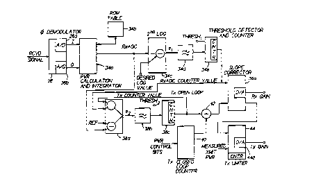
Fig. 2 is a bloclc diagram that shows in greater detail the
digital AGC and transmitter power control circuits of Fig.
Fig. 3 is a schematic diagram showing a ROM-based look-up
circuit (34a of Fig. 2) for determining received signal
power;
20 Fig. 4 illustrates in greater detail the block 38a of Fig.
2 ;
Fig. 5 is a block diagram of a presently preferred
embodiment for implementing the blocks 38a and 38b of Fig.
2 5 2: and
Fig. 6 is graph that illustrates the effect of a scaling
block that is shown in Fig. 5.
DETAILED DESCRIPTION OF T~IE INVENTION
Reference is made to Fig l which illustrate a presently
preferred embodiment of a spread spectrum CDMA
radiotelephone l0 in accordance with this invention. As
35 will become apparent, certain ones of the blocks of the
radiotelephone l0 may be implemented with discrete circuit
elements, or as software routines that are executed by a
suitable digital data processor, such as a high speed
-
WO 96/10298 2 1 ~ ~ 5 9 5 PCT~ 595/12180
signal processor. Alternatively, a combination of circuit
elements and software routines can be employed. As such,
the ensuing description is not intended to limit the
application of this invention to any one particular
5 technical embodiment.
In the preferred embodiment of this invention the
radiotelephone 10 operates in accordance with the TIA/EIA
Interim Standard, Mobile Station-Base Station Compatibility
10 Standard for Dual-Mode Wideband Spread Spectrum Cellular
System, TIA/EIA/IS-95 (July 1993). However, compatibility
with this particular interim standard is not to be
considered as a limitation upon the practice of this
invention .
The radiotelephone 10 includes an antenna 12 for receiving
RF signals from a cell site, hereafter referred to as a
base station (not shown), and for transmitting RF signals
to the base station. When operating in the digital (CDMA)
20 mode the RF signals are phase modulated to convey speech
and signalling information. Coupled to t~le transmitter 12
are a gain controlled receiver 14 and a gain controlled
transmitter 16 for receiving and for transmitting,
respectively, the phase modulated RF signals. A frequency
25 synthesizer 18 provides the required frequencies to the
receiver and transmitter under the control of a controller
20. The controller 20 is comprised of a slower speed MCU
for interfacing, via a codec 22, to a speaker 22a and a
microphone 22b, and also to a keyboard and a display 24. In
30 general, the MCU is responsible for the overall control and
operation of the radiotelephone 10. The controller 20 is
also preferably comprised of a higher speed digital signal
processor tDSP) suitable for real-time processing of
received and transmitted signals.
The received RF signals are converted to base band in the
receiver and are applied to a phase demodulator 26 which
derives in-phase (I) and quadrature (Q) signals from the
21 9~595 IPEA/US 1 6 s~P ~g9c
received signal. The I and Q signals are converted to
digital representations by suitable A/D converters (26a and
16b of Fig. 2) and applied to a three finger (Fl-F3)
demodulator 28. Each of the fingers includes a local PN
5 generator. The output of the demodulator 28 is applied to
a combiner 30 which outputs a signal, via a deinterleaver
and decoder 32, to the controller 20. The digital signal
input to the controller 20 is expressive of speech samples
or signalling information. The further processing of this
10 signal by the controller 20 is not germane to an
understanding of this invention and is not further
described, except to note that the signalling information
will include transmitter power control bits that are sent
from the base station to the radiotelephone 10.
The I and Q signals output from the I-Q demodulator 26 are
also applied, in accordance with this invention, to a
receiver digital AGC block 34 which processes same, in a
manner described below, and which produces an output signal
20 to an amplifier slope corrector block 36. One output of the
slope corrector block 36 is the RX GAIN signal which is
used to automatically control the gain of the receiver 14.
The output of the receiver digital AGC block 34 is also
25 applied to a TX open loop power control block 38. A TX
closed loop control block 4 0 inputs the received
transmitter power control bits from controller 20. An adder
42 adds the output of the TX open loop control block 38 to
the output of the TX closed loop control block 40 and
30 generates a sum signal which is applied to the slope
corrector 36 and, thence, to a TX limiter block 44. The
output of the TX limiter block 44 is the TX GAIN signal
that is applied to the transmitter 16 to control the output
power thereof.
An input to the transmitter 16 (vocoded speech and/or
signalling information) is derived from the controller 20
via a convolutional encoder, interleaver, Walsh modulator,
AMENDE~) SHEF~
WO 96/10298 2 1 9 ~ 5 9 5 PCT/US95/12180
11
PN modulator, and I-Q modulator, which are shown generally
as the block 46.
Before describing in detail the construction and operation
s of the receiver digital AGC block 34, the slope corrector
36, and the open and closed loop transmitter blocks 38, 40,
42 and 44, it is first noted that an optimally sampled
signal received from a base station having all ~h~nn~ t
operational will have a dynamic range of approximately
lO 64/l, or 18 dB. In addition, a fast fade can have a
dynamic range of approximately + 6 dB to -34 dt3. Unless
the receiver AGC is capable of perfectly tracking the fast
fade, there is a high probability that the signal will be
olipped by the receiver's A/D converter or that the signal
15 will be too small for the A/D converter (A/D urlderflow).
11owever, the clipping is generally symmetric and can be
~olerated to a certain extent. As such, a receive1- AGC step
response time constant of O. 5 milliseconds (ms) to 2 ms is
believed to be adequate for the receiver AGC to adequately
20 track fast fading, and to prevent clipping and A/D
converter overflow and underflow.
Consequently, it will be shown that this invention also
provides a receiver AGC function with a high tracking rate
25 capability when either signal amplification or attenuation
is required.
Reference is now made to Fig. 2 for a detailed description
of the receiver AGC and transmitter power control Eunctions
30 that were briefly mentioned above in the description of
Fig. l. In Fig. 2 the sub-components of the RCVR AGC 34 are
designated as 34a-34e, and the sub-components of the TX
open loop power control 38 are designated as 38a-38c.
35 Based on the digital outputs (A/Ds 26a and 26b) of the I-Q
phase demodulator 26 the power of the I and Q santples are
calculated by block 34a at least once per chip and
preferably twice per chip by, for example, a ROM table 34b
- Wo 96/10298 2 1 9 8 5 9 5 rcr/usgs/l2l8o
12
lookup. The calculated powers are integrated over a
predetermined period corresponding to, by example, one
symbol (64 chips). The integrated output signal is
designated as Rx AGC or as RxAGC herein.
One suitable technique for determining the received signal
power, when sampled once per chip, that is based on the ROM
lookup is as follows. Reference is also made to Fig. 3.
The outputs of the 6-bit A/Ds 26a and 26b are time
multiplexed and used as an address into the ROM 34b. Hence
the address space of the ROM is 26=64. The content of the
ROM 34b at each address is the square of that address,
i.e., if the output of one of the A/Ds is "25", then the
ROM content at address 25 is 625. The largest possible
positive output of one of the A/Ds is "31" which squared is
961. Similarly, the largest possible negative output of
one of the A/Ds is "-32" which squared would be 1024. This
number is, however, truncated to 1023. As a result, the
20 data output width requirement of the ROM 34b is limited to
10 bits, and the total ROM size is thus 64x10 bits.
The output of the ROM 34b is connected to an integrator,
which is comprised of an adder 35a and a register 35b. The
25 register 35b is clocked by a 2X chip clock, which also
clocks the counter 35d, which counts 128 samples. The clock
signal also selects, with MUX 35e, between the I and Q A/Ds
26a and 26b, respectively. As a result, the A/D outputs are
time multiplexed to the address inputs of the ROM 34b which
30 outputs in response the square of the A/D output value. The
ROM 34b output is then added to the value stored in the
register 35b, and the result of the addition is then stored
back into the register 35b. ~very 64th chip a second
register 35c is clocked to store the output of adder 35a,
35 while simultaneously clearing the first register 35b. As a
result, the second register 35c contains a value that
corresponds to the energy of 64 consecutive chips, or
symbol .
- WO 96110298 2 1 9 ~ 5 9 5 PCrlUS95112180
13
Referring again to Fig. 2, and in accordance with an aspect
of this invention, to obtain an equal rate of change when
increasing amplification, and also when decreasing
amplification, the power of the input signal (RX_AGC) is
5 not used directly, but instead the logarithm (any logarithm
base) of the signal is used.
More specifically, in the preferred embodiment of this
invention the second logarithm of the power is calculated
10 with a priority encoder 34c, wherein the second logarithm
is taken to be the position of the most signif icant set
bit. For example, with the 6-bit A/D converters 26a and 26b
the logarithm is scaled so that a power of o<=power<2
returns a zero, 2<=power<4 returns a 1, etc. Consequently,
15 each unit of the logarithmic value corresponds to 3 dB
power. Thus, an average input amplitude of 4 (out of the 6-
bit A/D converter space of 0-32) yields a linear power of
64x2x42 = 2048, which corresponds to a logarithmic value of
11 .
Furthermore, two more bits for the logarithm are calculated
by appending the two bits right of the most significant set
bit of the linear power value. Although this is a linear
approximation of the logarithm function, the error has been
25 found to be insignificant. The resolution of the power
measurement is thus approximately 0 . 75 dB.
The desired logarithm of the power (in the example above,
4xll = 44) is also subtracted from the calculated power in
30 the block 34c and the difference value (error signal e~) is
input to a single pole low pass filter 34d, the time
constant of which determines the speed of the overall
digital AGC circuit. By example only, a filter feedback
factor of 1-(31/32) yields a time constant of approximately
35 1.6 ms.
The output of the filter 34d is input to a threshold
detector and counter circuit 34~, where the filtered output
21 9~595
WO 96110298 PCr/US9511218~)
14
is monitored once per symbol by comparing same to a f irst
threshold value THRESH1. If the filtered output is found to
exceed the first threshold, the counter (CNTR) is
incremented or decremented depending on the sign of the
5 exceeded threshold. Simultaneously, the filter accumulator
is reset. For a theoretically correct operation, the filter
accumulator should be set to the opposite threshold. That
is, if the positive threshold is -x~ eed~d the counter
counts up and the f ilter register is set to the negative
lO threshold. However, this may cause the counter to
immediately count in the opposite direction. Therefore, it
is preferred to employ some degree of hysteresis. In the
preferred embodiment, +/- 0.16667 is used as a threshold
and +/- 0.125 as the reset value. To provide even more
15 hysteresis the filter accumulator could be reset to zero.
The output of the counter is eventually fed to a D/A
converter contained within the slope corrector block 36,
which outputs a signal Rx GAIN to control the receiver
amplifiers .
In that a unit change in the input and output of the f ilter
34d corresponds to a 3 dB change in power, the threshold
(THRESH1) is preferably set to +/- 0.33333 (ldB) for an AGC
step size of 2 dB, or to +/- 0.166667 (0. 5 dB) for an AGC
25 step size of l dB. That is, the value of THRESH1 is a
function of the desired receiver AGC step size.
The receiver AGC signal reaches a stable value when
negative values of the logarithm occur as frequently as
30 positive values at the input to the lowpass filter 34d. An
optimal steady state of the AGC occurs when there exists a
signal headroom of 6-12 dB in the A/D converters 26a and
26b. Because of the limited number of bits, the steady
state headroom may best be determined empirically for a
35 given application.
Although there exist several possible techniques for
altering the signal headroom in the A/D converter, a
Wo 96/10298 2 1 9 8 5 9 5 pcT/usgs/l2180
presently preferred technique alters the expected value of
the logarithm of the input power. It is noted that
parameters for the transmitter AGC determination may have
to be changed simultaneously, as will be described below.
The transmitter digital AGC function 38 has a similar step
counter 38a as the receiver AGC step counter 34e. The
transmitter AGC step counter value is subtracted from the
step counter value of the receiver AGC to form a second
error signal (e2). The error signal e2 is lowpass filtered
in a single pole low pass filter 38b, the time constant of
which is chosen so that the total time constant for the
transmitter AGC function is approximately 30 ms. A filter
feedback ratio of 1-(1023/1024) provides this time
constant.
The step size of the transmitter AGC is preferably no
larger than 0.125 dB. As such, and assuming a 1 dB step in
the receiver AGC signal (Rx_AGC), the Rx AGC counter value
output from 34e is left-shifted by three before the
difference is determined.
This technique will in and of itself yield an accuracy of
1 dB in the transmitter AGC signal. To achieve better
accuracy, the power integrated over one symbol (Rx_AGC) is
used instead. A precalculated expected value of the power
integrated over one symbol is subtracted from the actual
integrated power value and the result is filtered in the
above mentioned lowpass filter 38b. As before, this means
that the logarithm function is approximated with a linear
function. Following the example presented above, if the
desired logarithmic value is 44, then the linear average
power of the signal will have a variation of 1 dB and thus
have a value between 2048 and 2578 and, consequently, the
desired linear power value is set to (2048+2560)/2 = 2313.
In that the input to the filter 38b of 1 dB corresponds to
a value of 8; this input is shifted right by 6 ( (10-1 _
l)x2048 = 530 ~ 512, 512/8 = 64 => 6 right shifts).
Wo 96/10298 2 1 9 8 5 9 5 PCTN~ss/12180
If the signal headroom in the receiver A/D-converters 26a
and 26b is changed by changing the expected value of the
logarithm of the received power, the above-mentioned
expected value of the linear power is also changed.
5 This is preferably accommodated by an appropriate
additional shifting of the linear power value. The
following Table lists appropriate values for this
additional shift, gi!ven the desired receiver power
logarithm .
Table
Average Received Additional
received power, power, shift of
amplitude linear logarithmic linear power
for Tx AGC
128 28 _4
1.4 256 32 -3
2512 36 -2
202.8 1024 40 -1
4 2048 44 (11*4) 0
5.6 4096 48
8 8192 52 2
11. 2 16384 56 3
25 16 32768 60 4
22.4 65536 64 5
32 131072 68 6
More particularly, the block 38a in Fig. 2 calculates the
30 difference between the values of the Rx counter (CNTR) in
block 34e and a Tx counter (CNTR) in block 38c. This
difference is then lowpass filtered and compared to the
threshold. If the threshold is exceeded, the counter of
block 38c counts up or down and the new value is fed back
35 to block 38a, where it is again compared to the Rx counter
value from block 34e. This process will continue until the
values of the RX and Tx counters are equal.
The block 38a also calculates the difference between the
40 received linear power from block 34a and a predetermined
fixed value (REF). This difference is also fed to the
lowpass filter 38b. As a result, there are two input values
to the filter 38b for each process iteration.
Wo 96/10298 2 1 9 8 5 9 5 PCT/US95/12180
17
In this regard, and referring to Fig. 4, the function of
the receiver chain (blocks 26a-b and 34a-e) is to maintain
the average input amplitude constant to the A/D converters
26a and 26b. By example, assume that the desired absolute
5 amplitude corresponds to an A/D-output of 8 (out of the A/D
absolute range of 0-32). Then after integration the
measured power would be 82x128=8192. This value is thus a
predetermined fixed reference value (linear power
ref erence ) .
According to the preferred implementation of this
invention, one step in the output of the counter 34e
corresponds to a gain change of 1 dB, and one step in the
output of the counter 38c corresponds to 0.125 dB. Hence,
the output of counter 34e should be multiplied by 8 (left-
shifted by 3 in block 39a) before the subtraction of the
TxAGC counter value by block 39d. The switches 39e and 39f
function as multiplexers to connect the TxAGC counter value
and the shifted RxAGC counter values to the subtractor 39d,
or to connect a shifted Rx linear power value and a shifted
linear power reference value to the subtractor 39d.
Disregarding for a moment the Linear Power REF and the
RxAGC linear output, the Tx Open Loop would be in
equilibrium when the value of the RxAGC counter 34e, times
8, is equal to the value of the TxAGC counter 38c. Although
the Tx counter can have any value when in transition, in
any steady state its output has a value that is n x 8, that
is, the Tx Open Loop would has a steady state resolution of
8 x 0.125 = 1 dB. However, this resolution is not
sufficient to fulfill the requirements of the IS-95
specif ication .
To enhance the resolution, the invention employs the
difference between the linear power value and its
corresponding reference value. Here the power is expressed
linearly rather than in dB, wherefore first a linear
approximation of the logarithmic function is made. Since
WO 96/10298 2 1 9 8 5 q 5 Pcllus9sll2l8o
18
the intention is to enhance the resolution, the counter
difference is made to handle the large gain difference, and
limit the difference between the linear power value and the
reference to 3 dB.
Realizing now that 3dB corresponds to a linear value of 2,
2 dB corresponds to 1. 58 - 1. 5; 1 dB corresponds to 1. 2589
- 1.25; 0.5 dB corresponds to 1.122 - 1.125; 0.25 dB
corresponds to 1.0593 - 1.0625; 0.125 dB corresponds to
1.0292 - 1.03125, etc.; it can thus be seen that so long as
the difference is smaller than 3 dB, a doubling in the dB
number corresponds to a doubling of the fractional in the
linear number.
If a definition is made that 0 dB corresponds to 1 x 8192,
then 0 .125 dB is 1. 03125 x 8192 w 8448 . Therefore, with
the linear approximation, a gain change of 0.125 dB
corresponds to a change of 256 in the linear power value,
a gain change of 0 . 25 dB corresponds to a change of 512,
2 0 etc .
Above it was stated that a unit step change in the TxAGC
counter 38c corresponds to a gain change of 0.125 dB.
Hence, since in the linear difference 0.125 dB corresponds
to 256, the linear difference is divided by 256 (right-
shifted by 8 in block 39b) before being input to the filter
38b.
Suppose now that the RxAGC and the TxAGC counters have the
values 24 and 192 (8x24), respectively. For this case the
average input power changes from the desired value of 8192
to 8448, i.e. a gain change of 0.125 dB. The receiver
counter 34e will not react to this gain change, since the
change is smaller than 1 dB. However, the linear
difference that is input to filter 38b will be (8192-
8448)/256 = -1. After a period of time, depending on the
time constant of the filter 38b, the TxAGC counter 38c will
count down one step to 191. Hence the difference between
WO 96/10298 ~ 5 PCT/US95111180
19
the counters will be 8 x 24 - 191 = 1. The two inputs to
the filter 38b now cancel each other, but the transmitter
gain has decreased by 0.125 dB That is, the circuit has
increased the resolution of the TxAGC to 0.125 dB, which
5 fulfills the specification.
It should be noted that the linear approximation does ~ot
work equally well for negative gain changes, because -1 dB
corresponds to 0.794, but should be 0.741, -2 dB
corresponds to 0.630, but should be 0.415 etc. That is, the
linear approximation works best for differences smaller
than -2 dB. Also, as previously explained, the true
reference value should be (10-1 x 8192 + 8192)/2 = 9252
rather than 8192. However, although the former is actually
15 used in the subtraction, the latter is used in the scaling
of the approximation (the division by 256). The correct
scaling value would be 10313/8192 x 256 = 322, but this
would result in a rather cumbersome hardware
implementation. This leads to a small error in the
20 approximation, which in fact is partly cancelled by the
fact that a larger error may exist for negative gain
changes than for positive gain changes.
In summary, it is preferred to provide two inputs to the
25 filter 38b so as to enable a relatively large step size in
the RxAGC to be able to cancel fast changes in the input
signal level. On the other hand, the TxAGC is required to
be slower and more accurate. If the TxAGC followed only the
RxAGC, the resolution of the TxAGC would not be adequate.
30 However, by introducing the linear power value from block
34a, and its equivalently shifted linear power reference
value (block 39c), it becomes possible to increase the
accuracy of the TxAGC to the re~quired level.
35 While the above description serves to describe the
operation of the invention, it should be noted that a
number of possible implementatic~ns exist. For example, Fig.
5 illustrates a presently pref orred implementation where
Wo 96110298 2 ~ 9 8 5 9~ PCT/US95112180
blocks 38a and 38b are integrated, thus enabling a
substantial hardware savings.
The embodiment of Fig~ 5 includes a 5 to l multiplexer 50,
a l/x scaling circuit 52 (by example, x=1024), an
adder/subtracter 54, and a filter (D-flop) 56. A register
58 can be employed to store the output of the filter 56. A
state machine 60 controls the overall operation and timing
of these components. The overall transfer function of the
lo circuit shown in Fig. 5 resembles a one pole IIR filter.
The value of x may be made programmable. In general, the
value of x affects the response time of the circuit (and
hence the transmitter power level ) to a step change in the
input receive level, as indicated in the exemplary graph of
Fig. 6.
Referring again to Fig. 2, the output of the transmitter
AGC filter 38b forms the total open loop power estimate. As
has been described, this estimate is applied to a
20 comparator 38c which detects, by comparison with a second
threshold (THRESH2) if the step threshold is exceeded, in
which case the internal TX counter is incremented or
decremented, depending on the sign of the threshold
exceeded. Since one unit in the filter 38b input and
25 output corresponds to 0.125 dB, and this value is also the
step size of the TxAGC, the bipolar threshold (THRESH2) is
preferably in the range of +/- 0 . 5 .
A second counter 40 is used to count the closed loop power
30 steps output from the controller 22, and the output of the
counter 40 is added to the output of the counter in 38c
with the adder 4 2 .
A transmitter AGC step size of 0 . 5 dB has been found to
35 fulfill the requirements of the CDMA interim specification,
assuming ideal analog hardware. However, and following the
same reasoning as for the receiver AGC, a step size of
0.125 dB, with a lO-bit D/A-converteF 44a, is preferred.
WO 96/10298 2 ~ 9 ~ 5 9 5 PCTIUS95/12180
21
A presently preferred conversion rate for the A/Ds 26a and
26b is 9 . 6 kHz, since the position of the closed loop power
control bits vary and are required to be placed into effect
within 500 microseconds of receipt. However, other
conversion rates are within the scope of the teaching of
this invention.
The Tx Limiter block 44 operates in a manner similar to a
comparator and a switch The input to block 44 is the
amplification value that the Tx AGC algorithm has
determined to be appropriate. This amplification value is
compared to a preset value that represents the highest
possible amplification allowed (by the standard and/or by
the design). If the amplification exceeds the preset
value, the preset value will be output through the DAC,
rather than the calculated amplification. In this manner
the output power of the terminal 's transmitter is limited
to a predetermined maximum value. Furthermore, this maximum
output power level is made adaptive. Hence, the preset
value is replaced by a value from a further counter (CNTR).
The input of block 44 is compared to the counter value. If
the input exceeds the counter value, the counter value is
output. Simultaneously the counter is enabled to count up
or down one step. The direction of counting is determined
by a 1-bit signal from the RF section, where a comparison
is made whether a detected absolute output power level
exceeds the maximum allowed output level. In this way the
Tx AGC determination is tied to the actual absolute output
power level, and the adaptivity ensures that the maximum
output power level is fixed despite differences in
temperature and component tolerances.
The details of the operation of the Tx Limiter 44 is
described in commonly assigned U.S. Patent Application
Serial No. 08/303,619, filed September 9, 1994, entitled
"Spread Spectrum Radiotelephone having Adaptive Transmitter
Gain Control" by Lars ~lucke et al. (Attorney's docket no.
309-934809-NA) .
WO96/10298 2 1 9 a 5q5 PCINS95/12180
22
The receiver and transmitter power amplifiers typically
require a slope correction to be applied to their
respective gain control signals. For this purpose, the
unsigned output from the step counter 34e and the sum of
5 step counters 38c and 40 are transformed into two's
complement numbers by inverting the sign bits. Each 2 ' s
complement number is then multiplied in block 36 with a 7-
bit number to correct the amplification slope.
lO If it is assumed that a maximal error of 50% in the power
amplifier slopes exist, then the value of the 7-bit number
should be between O . 5-l. 5 => -2 to 2, since the multiplier
must be able to perform 2 ' s complement multiplications .
Consequently the LSB corresponds to l/32 and the error
15 after the correction is maximally l/64 or l . 56~i .
-
For the case where an S-curve transmitter correction is
desired, the dynamic range is divided into a plurality
(e.g., 4,8,16 etc.) of subranges, each subrange having its
20 own correction factor. The 2 (or 3, 4 etc. ) most
significant bits are then used to select the correct
correction factor subrange.
A presently preferred embodiment of this invention has thus
25 been described. However, a number of modifications could be
made to this embodiment, and these modifications would
still be within the scope of the teaching of this
invention. By example, other values and ranges of values
could be employed for the various thresholds that are used
30 to increment and decrement the counters in blocks 34e and
38c. Further by example the look-up table 34b can be
embodied within any suitable type of memory device, such as
a FAM that is loaded with suitable values by the controller
20. Also, any reference to a counter or a counter value can
35 also be read to include a register or register value. By
example, a memory location can be incremented and
decremented under software control and may therefore be
Wo 96/10298 2 1 q 8 5 9 5 PCrlUS95/~2180
23
functionally equivalent to a counter, such as a decade or
binary counter device or circuit.
Furthermore, the teaching of this invention can be employed
5 with RF transceivers in general, including Time Division
Multiple Access-type transceivers, and is not restricted
for use only with spread spectrum and/or CDMA tranceiver
types. Also, it should be realized that the power can be
integrated over any suitable time period, and need not be
lO integrated over only a period corresponding to one symbol.
Thus, while the invention has been particularly shown and
described with respect to preferred embodiments thereof, it
will be understood by those skilled in the art that changes
15 in form and details may be made therein without departing
from the scope and spirit of the inve~tion.