Note: Descriptions are shown in the official language in which they were submitted.
0 2 1 9 9 4 5 6
WIRELESS COMMUNICATION DEVICE
WITH ANTENNA-ACTIVATED SWITCH
Field of the Invention
The present invention relates generally to the field of wireless
communication, and more particularly to a wireless communication device.
Although the invention is subject to a wide range of applications, it is
especially suited for use in a handheld radiotelephone, and will be
particularly described in that connection.
Background of the Invention
Radiotelephones having a retractable compound antenna are known
in the art. Published Canadian Patent Application No. 2,036,677 describes
a radiotelephone having an extendible antenna that is capable of receiving
signals in both the extended position and retracted position. This
application, however, does not address the impedance imbalance of the
antenna in its respective extended and retracted positions, or a solution for
providing a matching state between the radio transceiver and antenna.
This patent application, as well as US Patent No. 5,177,492, also
describe rod antenna mounting mechanisms attached to the casing of the
radiotelephone, which grip the rod antenna to hold it in an extended or
retracted position. The compound antennas used in the mechanisms are
relatively rigid where a helix joins the rod, because the juncture of rod and
helix is also the point that is electrically coupled to the radio feed terminal
when the antenna is in the retracted position. Consequently, they have the
problem of being easily damaged at the juncture when the radiotelephone is
dropped .
Because retractable, compound antennas typically have a long
flexible linear antenna element, this element needs to be guided into the
radiotelephone. It is known to use a well formed out of the casing to guide
the linear antenna element, such as described in US Patent No. 5,177,492.
This technique has the disadvantage of increasing the bulk and weight of the
radiotelephone. Another known technique is to attach a straw-like tube to
-2 -0 2 1 9 9 4 5 6
the casing. This technique has the disadvantage of requiring an assembly
step specific to the casing, which otherwise would not be required. Another
known technique is to attach the straw-like tube to the circuit board that
already has many assembly steps associated with it. This technique has the
5 disadvantage of requiring additional fastening components to be added and
assembled to the circuit board, specific for the purpose of holding the straw,
to an already crowded circuit board.
There are also known radiotelephones, as described in US Patent
No. 5,374,937, having an extendible antenna that uses a single matching
10 circuit and a first feed terminal to couple an inner circuit to the antenna in the
extended position, and then bypass the matching circuit in the retracted
position by coupling the inner circuit to the antenna in the retracted position
by way of a second feed terminal disposed a distance from the first feed
terminal. This technique has the disadvantage of requiring two feed
15 terminals. It further has the disadvantage that the antenna portion between
the two feed terminals radiates inside the housing, possibly interfering with
sensitive electrical components disposed inside the housing.
Radiotelephones having a retractable compound antenna and a
variable impedance matching circuit and single feed terminal are known in
20 the art. One example of such known radiotelephones described in US
Patent No. 5,335,368 and another is embodied in Model No. TZ-820B
provided by NEC. This latter radiotelephone has a variable impedance
matching circuit coupled with antenna, wherein the matching circuit consists
of two parallel circuit paths, each path having a unique reactance. These
25 circuit arrangements are shown in FIG. 1. The parallel circuit paths of a
matching circuit 10, having reactive components L1, L2, and C, are selected
in response to the position of an antenna 12 in order to match the
impedance of antenna 12 to the impedance of a coaxial connector 14. The
selection is made by a double-pole, double-throw switch 16 arranged so that
30 the switch is thrown by lower end of antenna 12 forcing mechanical contacts,
S, from a normally open position to a closed position as antenna 12 is
moved from the extended position, shown in solid lines, to the retracted
position, shown in dotted lines. The antenna 12 is held in its respective
3 0 2 ~ 9 9 4 5 6
positions by a holding member 22 attached to a housing 24 of the
radiotelephone, and guided by a conductive tube 20. Holding member 22
further functions to electrically couple the switch to the antenna. In addition
to requiring a switch and a multipath matching circuit, a termination
impedance 18 coupled between ground and one end of antenna 12, and the
ground-coupled conductive tube 20, are necessary to provide the matching
in the retracted position.
This matching technique is not suitable for all handheld
radiotelephones. For example, it requires additional components in the
matching circuit to provide the two connection states for matching; and it
requires a relatively bulky switch to make the connection states. These
additional components increase the size of the radiotelephone, which can
be a handicap as radiotelephones become smaller. Furthermore, the switch
increases the probability of a faulty connection in the sensitive transmission
and reception signal path. It further has the disadvantage of requiring an
additional termination impedance and conductive tube.
A need therefore exists for a handheld radiotelephone that provides a
matching state between the transceiver and retractable compound antenna
in both its positions, and does so with an elegant design that increases
reliability and manufacturability by reducing the number and complexity of
components and moving mechanical parts. A need also exists for a
handheld radiotelephone that is not easily damaged when dropped at the
point where the rod joins the helix.
Furthermore, a need exists for a radiotelephone having a switch that
can be activated by the position of the radiotelephone's retractable antenna,
and minimizes the addition of mechanical switching parts in the signal path
from the antenna to the transceiver.
-4-0 21 99 4 5 6
Brief Description of the Drawings
FIG. 1 is a general electrical schematic of a conventional matching
circuit arrangement.
FIG. 2 is a general electrical schematic of a first embodiment of a
radiotelephone configured according to the invention.
FIG. 3 is a right-side elevation view of a second embodiment of a
radiotelephone configured according to the invention, with a partial section
view showing certain internal components of the radiotelephone.
FIG. 4 is a front, bottom, and right-side perspective view of a circuit
0 board, terminals, and an antenna assembly of the radiotelephone shown in
FIG. 3.
FIG. 5 is a cross section view of the antenna and the bushing shown
in FIG. 4.
FIG. 6 is a fragmentary front elevation view of the circuit board, a feed
terminal, and portions of the antenna assembly shown in FIG. 4, when the
antenna is in an extended position.
FIG. 7 is a fragmentary cross section view of the circuit board, a
ground terminal, and portions of the antenna assembly shown in FIG. 4,
when the antenna is in the retracted position.
FIG s. 8 and 9 are fragmentary cross section views of the circuit board,
a feed terminal, and portions of the antenna assembly shown in FIG s. 3 and
4, when the antenna is in the extended or retracted position, respectively.
FIG. 1 0 is a general electrical schematic of third embodiment of a
radiotelephone configured according to the invention.
FIG. 11 is a general electrical schematic of fourth embodiment of a
radiotelephone configured according to the invention.
Detailed Description of the Preferred Embodiments
The wireless communication device described herein provides
advantages over known handheld radiotelephones in that it provides a
matching state between the radio circuit and retractable compound antenna
in both the extended and retracted positions, and does so with a design that
reduces the complexity of the matching circuit and switch.
5 0 2 1 9 9 4 5 6
These advantages over the conventional radiotelephones are
principally provided by a single matching circuit, a single feed terminal, and
a switch that bypasses, or shorts out, the matching circuit.
In general terms, when the antenna is in its extended position, the
switch is open, and thus the matching circuit is coupled in series between
the antenna assembly and the radio circuit. In this configuration, the
matching circuit functions to match the high impedance of the antenna
assembly (approx. 400 to 600 ohms) to the impedance of the radio circuit
(approx. 50 ohms). Conversely, when the antenna is in the retracted
position, the switch is closed, and thus the matching circuit is either
bypassed and does not perform a matching function, or is bypassed and
reconnected in parallel with the antenna to assist in providing a matching
function.
As illustrated in FIG. 2, in one such embodiment configured according
to the present invention, a wireless communication device, e.g., a
radiotelephone 20, comprises a housing 22; a circuit board 24, an antenna
assembly 26, a radio circuit 28, a matching circuit 30, a switch 32, a ground
plane 34, a feed terminal 36, and a ground terminal 38 coupled with a
ground. Circuit board 24 is disposed inside housing 22, and radio circuit 28,
matching circuit 30, switch 32, ground plane 34, feed terminal 36, and
ground terminal 38 can be disposed on circuit board 24.
Antenna assembly 26 includes a bushing 40 and an antenna, e.g., a
compound antenna 42 having a first antenna portion, e.g., at least a helicoil
44, and a second antenna portion, e.g., at least a portion of the rod 46. The
first antenna portion is carried by the second antenna portion and can be
electrically coupled, e.g., by direct electrical contact, to the second antenna
portion. Bushing 40 can be affixed to housing 22, and compound antenna
42 is moveable within bushing 40 from a retracted position as shown in FIG.
2 to an extended position.
In the extended position the first antenna portion is located outside of
the housing and the second antenna portion is substantially located outside
of the housing. Further, a first coupling location 45 of the antenna, e.g., the
lower end of the second antenna portion, is electrically coupled, e.g., in
-6 - 0 2 1 9 9 4 5 6
direct electrical contact, with feed terminal 36. In the retracted position, thefirst antenna portion is located substantially outside of houlsing 22, and the
second antenna portion is located inside housing 22 and in close proximity
to ground plane 34. Further, feed terminal 36 is electrically coupled, e.g., in
direct electrical contact, with a second coupling location 47 of the antenna,
e.g., the lower end of the first antenna portion, and ground terminal 38 is
electrically coupled, e.g., in direct electrical contact, with first coupling
location 45.
Compound antenna 42 has many parameters representative of the
position of the compound antenna 42. For example, the physical location of
compound antenna 42 relative housing 22 or feed terminal 36, the electrical
impedance of compound antenna 42, or the strength of the electrical signal
that compound antenna 42 receives.
Radio circuit 28 can be, e.g., a duplexer, a transmitter, a receiver, a
modulator, a demodulator, or traces connecting the components of radio
circuit 28, or some combination of these components and traces.
Matching circuit 30 is coupled between feed terminal 36 and radio
circuit 28. Matching circuit 30 can be, e.g., a T-connected circuit with a
capacitor C in one arm, an inductor L1 in the other arm, and a ground-
terminated inductor L2 in the leg.
Switch 32 is electrically coupled between feed terminal 36 and radio
circuit 28 in a parallel configuration to matching circuit 30. Switch 32 is
operative to change state in response to a predetermined variation of the
antenna's parameter, whereby switch 32 can redefine or rearrange matching
circuit 30 when switch 32 changes state. When switch 32 is in one state,
radio circuit 28 is directly coupled with feed terminal 36, in parallel with thereconfigured matching circuit. When switch 32 is in another state, radio
circuit 28 is coupled with feed terminal 36 through matching circuit 30.
Although switch 32 and matching circuit 30 are shown as separate
components in FIG. 2, switch 32 can be a sub-component of matching circuit
30, or a sub-component of other components of radiotelephone 20.
Switch 32 can include, e.g., a single-pole, single-throw switch.
Switch 32 can also include a sensor 48, or the sensor can be external to
7- 02199456
switch 32. Sensor 48 detects a predetermined variation of the antenna's
parameter. Sensor 48 can be, e.g., the arm of the single-pole, single-throw
switch that is normally open when the antenna is extended, and that is
mechanically moved to the closed position by physical contact with the lower
5 end of the second antenna portion. Accordingly, the parameter is the
retractable antenna's position relative to housing 22 or feed terminal 36, and
the predetermined variation is movement to a position that moves the switch
to the closed position. Alternatively, it can be, e.g., a proximity sensor that
measures the antenna location, a relative strength signal indicator that
measures the strength of the signal received by compound antenna 42, or
an impedance bridge that measures the impedance of compound antenna
42. Under each alternative, the sensor sends a control signal to switch 32,
and switch 32 can change state in response to the control signal.
Regarding the electrical characteristics of the antenna, the impedance
of the antenna in the extended position has a first impedance as viewed from
feed terminal 36. In the retracted position, the antenna has a second
impedance as viewed from feed terminal 36 that is the parallel combination
of the impedance of the first antenna portion and the second antenna
portion. Moreover, because the switch is closed in the retracted position, the
matching circuit is reconnected and coupled between feed terminal 36 and
ground, placing it in a parallel connection with the first antenna portion and
the second antenna portion. Consequently, matching circuit 30 can be
chosen not only to substantially match the first impedance of the antenna
when in the extended position to the impedance of radio circuit 28 (when
matching circuit 30 is in series with feed terminal 36 and radio circuit 28), but
also to assist in matching the second impedance of the antenna when in the
retracted position to the impedance of radio circuit 28. Furthermore, one of
ordinary skill in the art will appreciate that the switch can be in a closed state
when the antenna is in a first position, e.g., extended, and in an open state
when the antenna is in a second position, e.g., retracted, and,
correspondingly, the matching circuit in parallel when the antenna is
extended and in series when the antenna is retracted.
- 8 0 2 1 9 9 4 5 6
The technique for selecting the first impedance of the antenna, the
second impedance of the antenna, and the matching circuit to substantially
match the first impedance of the antenna and also, when reconnected, to
assist in matching the second impedance of the antenna, are readily
understood by one of ordinary skill in the art.
For example, if the compound antenna is chosen to have an electrical
length of a half wavelength, first impedance in the extended position can
have a range of about 400 ohms to about 600 ohms at operating
frequencies. If radio circuit 28 has an impedance of approximately 50 ohms,
or other value characteristic of radio circuit 28, matching circuit 30 can be
selected that substantially matches the first impedance of the antenna to the
impedance of radio circuit 28.
Furthermore, if the first antenna portion is, e.g., helicoil 44 and a
small segment of rod 46 chosen to have an electrical length of a quarter
wavelength, first antenna portion will have a first impedance of about 50
ohms as viewed from feed terminal 36 in the retracted position. Further, if
the second antenna portion is, e.g., the remaining segment of rod 46 chosen
to have an electrical length of a quarter wavelength and is ground-
terminated via ground terminal 38 and placed in close proximity to ground
plane 34, the second antenna portion will appear as substantially an open
circuit having an impedance that is at least an order of magnitude greater
than the impedance of the first antenna portion. Consequently, the second
impedance of the antenna in the retracted position is substantially the
impedance of the first antenna portion alone, i.e., about 50 ohms. This 50
ohm impedance of radio circuit 28 substantially matches the about 50 ohm
second impedance of the antenna.
Accordingly, the reconnected matching circuit 30 is chosen so that it
does not contribute significantly to the matching, e.g., the impedance of the
reconnected matching circuit can have an impedance that is an order of
magnitude greater than the second impedance.
Those skilled in the art will recognize that various modifications and
variations, in addition to those already described, can be made in the
radiotelephone of the present invention and in construction of this
9 ~2~ 9~ 456
radiotelephone without departing from the scope or spirit of this invention.
As examples, the demarcation between the first antenna portion and the
second antenna portion can be defined by an area where feed terminal 36
couples with the antenna in the retracted position. Accordingly, the first
antenna portion can be any part of rod 46, or all of rod 46 and a part of
helicoil 44. Furthermore, the first antenna portion and second antenna
portion can be radiating elements of different shapes. Also, other
configurations of switches and a matching circuit can be used that places the
matching circuit in a series configuration with the radio circuit and feed
terminal in one configuration, and places the matching circuit in parallel with
the antenna in another configuration. And, instead of the second antenna
portion being a quarter wavelength, ground terminated and adjacent a
ground plane, it can be of a different wavelength, terminated with an
impedance, or surrounded by a conductive tube that is grounded. Also, the
feed contact and bushing can be the same component, and the feed contact,
ground contact, or the switch can be, e.g., disposed on the housing or a
component inside the housing.
Reference wili now be made in detail to a second embodiment of a
radiotelephone configured according to the present invention. Where
appropriate the same reference numerals are used to avoid unnecessary
duplication and description of similar elements already referred to and
described above.
FIG. 3 is a right-side elevation view of radiotelephone 20 configured
according to the invention, with a partial section view showing certain
internal components of the radiotelephone. This figure illustrates, among
other things, the physical relationship of antenna assembly 26 in the
extended position relative to housing 22 and to circuit board 24 disposed in
housing 22. In this embodiment, the antenna of antenna assembly 26
includes a linear radiating element 58 and helical radiating element 56
carried by an end of linear radiating element 58. In the extended position,
helical radiating element 56is located completely outside of housing 22, and
linear radiating element 58is located substantially outside of housing 22.
-1o-o2199456
FIG. 4 is a perspective view of antenna assembly 26 in the retracted
position, and highlights the physical configuration of antenna assembly 26 in
relation to circuit board 24, feed terminal 36, ground terminal 38. Also
shown as optional components of antenna assembly 26 are a tube 52 and a
5 tube support 54 that is affixed to circuit board 24 and holds one end of tube
52 in a fixed position. The other end of tube 52 is held in a fixed position by
ground terminal 38. As seen in the figure, ground terminal 38 and feed
terminal 36 are affixed near one side of circuit board 24, at opposite ends of
the side. In the retracted position, ground terminal 38 makes direct physical
10 and electrical contact with the first portion of the second portion of the
antenna, and feed terminal 36 makes direct physical and electrical contact
with the second portion of the second portion of the antenna. Also, bushing
40, which is affixed to housing 22 in this embodiment, is shown disposed
adjacent feed terminal 36.
Tube 52 can be composed of a nonconductive material, e.g., plastic,
and serves to guide the antenna from the extended position to the retracted
position, as the antenna moves through the interior of tube 52. Moreover,
tube 52 can be coated with a conductive material or be composed entirely of
a conductive material and coupled with a ground. In this configuration, tube
52 can be used act upon the first portion of the antenna as viewed from feed
terminal 36 so that it appears as a relatively high impedance relative to the tothe impedance of the second antenna portion of the antenna.
FIG. 5 is a cross section of the antenna and the bushing shown in
FIG. 4, illustrating the details of compound antenna 42 for this embodiment.
Helical radiating element 56 can include helicoil 44. Linear radiating
element 58 can include rod 46. Alternatively, helical radiating element 56
and linear radiating element 58 can be a combination of coil and rod
antenna elements. Helicoil 44 is fastened to an end of rod 46 by a suitable
means, e.g., an upper ferrule 64 that is crimped onto rod 46 and soldered to
an end of helicoil 44 as in this embodiment. Other suitable equivalent
means may be used to fasten helicoil 44 to rod 46, e.g., spot welding or
soldering the coil to the rod; press fitting or inserting the end of the coil into a
-11 - O 2 ~ 9 9 4 5 6
well formed in the end of the rod or a hole formed in the side of the rod; or
using the non-conductive material surrounding helicoil 44 to rod 46.
Lower ferrule 70 is affixed near or at end of rod 46; and a collar 66 is
affixed near the other end of rod 46, at a location below helicoil 44. The
ferrule and the collar can be fixedly attached to the rod by crimping or some
other suitable means. This physical attachment also provides direct
electrical coupling of lower ferrule 70 and collar 66 to rod 46. Accordingly
lower ferrule 70 serves as a first coupling location on the antenna, and collar
66 serves as a first coupling location on the antenna. Further, in this
particular embodiment, the first antenna portion extends from collar 66 to
include helicoil 44; and the second antenna portion extends from collar 66 to
the end of rod 46.
This particular structural arrangement facilitates the application of a
non-conductive material to the metallic parts of the antenna that are not
meant to be exposed, i.e., at least a portion of lower ferrule 70 and collar 66.For example, separating the second coupling location, i.e., collar 66, from
the means for connecting helicoil 44 and rod 46, i.e., upper ferrule 64, allows
the easy application of a coating 62 to helicoil 44, the segment of rod 46
between collar 66 and upper ferrule 64, a portion of collar 66, e.g., by an
injection molding process. Further, a sleeve 68 can also be applied to the
remaining portion of rod 46 by injection molding.
Although this particular embodiment shows collar 66 and lower ferrule
70 in direct physical and electrical contact with rod 46, a non-conductive
material or a dielectric material could separate the ferrule and/or collar from
rod 46, and thus be capacitively coupled with rod 46 and form part of the
coupling location. Further, the reactance of this capacitive coupling can be
considered as a part of the antenna's impedance as viewed from the feed
contact.
Furthermore, separating the second coupling location from the means
for connecting by a predetermined distance, e.g., the length of the bushing
40, also provides the advantage of removing added rigidity caused by
second coupling location being at the same point as the means for
connecting. This provides an advantage over known radiotelephones
-12(3 2 1 99 4 5 6
employing a compound antenna that, when the antenna is retracted, the
means for connecting is allowed to flex, thus preventing mechanical damage
to the junction when, e.g., the radiotelephone is dropped and the floor strikes
helical radiating element 56 to apply a torque to the means for connecting.
FIG. 6 is a fragmentary front elevation view of circuit board 24, feed
terminal 36, and portions of antenna assembly 26 shown in FIG. 4, when the
antenna is in an extended position. This figure illustrates, among other
things, the feature of feed terminal 36 not only being electrically coupled withthe antenna at a first coupling location, but also holding the antenna in
extended position.
In particular, the first coupling location, e.g., lower ferrule 70, has a
first section with a first thickness and a second section with a second
thickness that is greater than the first thickness. In this particular
embodiment, the first thickness is a first diameter of cylindrically shaped tip
78 of lower ferrule 70, and the second thickness is a second diameter of a
ring 72 formed on, or out of, lower ferrule 70. (See also FIG. 5.) Although
ring 72 encircles lower ferrule 70, the first section can be a bulge that only
extends partly around lower ferrule 70 or extends completely around as
does ring 72.
Feed terminal 36 including at least one flexible member, e.g., two
opposing flexible members such as wings 74 that act as leaf springs. The at
least one flexible member can also be a spring loaded device. The antenna
is moveable past the flexible members to and from the extended position
and the retracted position, the flexible members moving, due to irregularities
in the shape of the antenna, in a direction substantially perpendicular to the
movement of the antenna. Wings 74 apply an increasing force as they are
pushed outward away from the antenna, and are resilient and act to return to
their resting position. A lower end 76 of bushing 40, which can be
cylindrically shaped, has a diameter smaller than the second diameter, and
thus limits the motion of the antenna from the retracted position to the
extended position.
Further, in moving to the extended position, ring 72 passes through
wings 74 before the first section, the increase and then decrease in spring
-130 21 9 9 4 5 6
force exerted by wings 74 as ring 72 passes wings 74 provides tactile or
detent feedback to the radiotelephone that the antenna is fully retracted.
After ring 72 passes wings 74, wings 74 move inward to contact tip 78.
Consequently, ring 72 is held between wings 74 and lower end 76 of the
bushing by the force exerted by wings 74.
(The item labeled as reference numeral 86 that appears in FIG. 6 is
explained in the discussion corresponding to FIG. 8.)
One of ordinary skill in the art can appreciate that the means for
limiting the motion of the antenna to the retracted position can be
accomplished by other means, e.g., a second ring formed on the antenna,
and that the bushing is not necessary for wings 74 to hold the antenna. For
example, lower ferrule 70 can be formed with a concave ring encircling it,
and wings 74 resting in the concave ring can hold the antenna in the
extended position.
FIG. 7 is a fragmentary cross section view of circuit board 24, ground
terminal 38, and portions of antenna assembly 26 shown in FIG. 4, when the
antenna is in the retracted position. This figure illustrates, among other
things, the feature of ground terminal 38 not only being electrically coupled
with the antenna at the second coupling location, but also holding the
antenna in retracted position and holding tube 52.
Ground terminal 38 includes a rigid member 82 and a flexible
member 80. These two members can be integrally formed from a single
sheet of metal or be two individual elements constituting ground terminal 38.
rigid member 82 can be affixed to circuit board 24, as well as rigid member
82, and rigid member 82 can move relative to rigid member 82. Flexible
member 80 can be, e.g., a leaf spring or a spring loaded device, and can
move in a direction substantially perpendicular the rigid member. When the
antenna moves from the extended position to the retracted position, lower
ferrule 70 moves into ground terminal 38, and lower ferrule 70 forces the
flexible member to move in a direction substantially perpendicular to the
movement of the antenna.
Lower ferrule 70 has a bulge formed thereon, e.g., ring 72, and, as the
antenna moves to the retracted position, the bulge slides across flexible
14 021 99 456
member 80, which translates to an increased spring force applied to the
antenna that the radiotelephone feel and can realize that is reaching the fully
retracted position. After the bulge clears flexible member 80, the force on the
antenna is reduced, thus informing the user that the fully retracted position
has been reached. Flexible member 80 continues to exert a force against
the coupling location in the fully retracted position, and thus holds the first
coupling location against rigid member 82.
Moreover, rigid member 82 has an upturned end 88 that deflects the
end of tube 52 when tube 52 is inserted into ground terminal 38 during
assembly. Upturned end 88 pressing against the inserted end of tube 52
holds this end in place. Thus, a separate fastening means is not required to
hold the end of the tube, saving circuit board space and easing assembly.
FlGs. 8 and 9 are fragmentary cross section views of the circuit board,
a feed terminal, and portions of the antenna assembly shown in FlGs. 3 and
4, when the antenna is in the extended or retracted position, respectively.
These figures illustrate, among other things, the feature of an integral feed
contact and switch, which can be used as switch 32 shown in FIG. 2.
Circuit board 24 has a pad 84 formed on it. Pad 84 is one part of the
switch. This pad can be electrically coupled with, e.g., matching circuit 30, ormore particularly with L1.
Feed terminal 36 is affixed to circuit board 24 and can include a
member whose movement is operatively responsive to the antenna's
physical positions, e.g., a flexible arm 86 which acts as a leaf spring.
Flexible arm 86 and wings 74 can be formed from a single sheet of metal
using well-known stamping techniques. Flexible arm 86 is disposed relative
to pad 84 and forms another part of the switch. Flexible arm 86, or feed
terminal 36, can be electrically coupled with, e.g., matching circuit 30, or
more particularly with C.
Flexible arm 86 in its resting position projects into the path of the
antenna in its movement to and from the extended and retracted positions.
Accordingly, in this embodiment, the switch is normally open. Further, it is
disposed below wings 74, so that when the antenna is in the retracted
position, the switch is normally open. Other configuration are possibie. For
-15- ~ 2 1 99 4 5 6
example, if the electrical contact were located at the opposite end of the
circuit board, where ground terminal 38 is located in the illustrated
embodiment, the switch would be closed in the retracted position.
Because flexible arm 86 is disposed in the pathway of the antenna,
linear radiating element 58 contacts flexible arm 86 during its movement
from the retraced position and forces flexible arm 86 to contact pad 84. FIG.
9 illustrates flexible arm 86 contacting pad 84 to make direct electrical
contact. Consequently, when the antenna is in one of its two physical
positions flexible arm 86 is not electrically coupled with pad 84 to thus place
the switch in an open position; and when the antenna is in the other of the
antenna's two physical positions flexible arm 86 is electrically coupled with
pad 84 to thus place the switch in a closed position.
Furthermore, flexible arm 86 and collar 66 are arranged so that they
are in direct physical and electrical contact when the antenna is in the
retracted position. Accordingly, feed terminal 36 is electrically coupled with
the second coupling location.
A third embodiment the radiotelephone will now be described with
reference to the general electrical schematic shown in FIG. 10. Where
appropriate the same reference numerals are used to avoid unnecessary
duplication and description of similar elements already referred to and
described above. Only the significant differences of the third embodiment as
compared to the earlier described embodiment will be discussed hereafter.
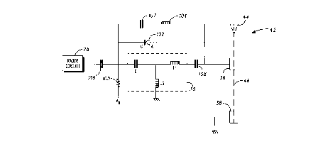
Fig. 10 particularly illustrates an alternative embodiment of switch 32.
Switch 32 comprises a diode 102 electrically coupled between feed terminal
36 and radio circuit 28 and in a parallel configuration to matching circuit 30.
Switch 32 further comprises sensor 48, which includes rod 46.
A bias voltage VB jS applied to the cathode of diode 102 via a resistor
100. VB jS negative with respect to ground potential. Furthermore, blocking
capacitors 106 and 108 are coupled between the bias voltage and radio
circuit 28 and compound antenna 42, respectively. An inductor 104 is
coupled to diode 102 in an electrically parallel configuration, and is
electrically coupled between feed terminal 36 and radio circuit 28. A
blocking capacitor 107 is coupled in series with inductor 104. Blocking
0 2 ~ 9 9 4 5 6
capacitor 107 allows a direct-current potential to be imposed across diode
102 without having any direct current through the parallel inductor 104. In
this particular embodiment, collar 66 and lower ferrule 70 are in direct
physical and electrical contact with conductive rod 46. (See FIG. 5).
The operation of switch 32 will now be described.
When the antenna is extended, feed terminal 36 makes direct
physical and electrical contact with lower ferrule 70. Blocking capacitors
106,107,108 block direct currents from entering radio circuit 28, compound
antenna 42, and inductor 104. Because there is no complete electrical path
from VB to ground, VB does not forward-bias diode 102.
When compound antenna 42 moves to the fully retracted position,
feed terminal 36 makes direct physical and electrical contact with collar 66,
and ground terminal 38 makes direct physical and electrical contact with
lower ferrule 70. Consequently, rod 46 bridges ground terminal 38 and feed
terminal 36 to form a complete electrical path from VB to ground. Direct
currerlt flow from the negative-valued VB through ground terminal 38, lower
ferrule 70, rod 46, collar 66, feed terminal 36, diode 102, and resistor 100.
Resistor 100 determines the magnitude of direct current flowing through
diode 102.
The forward-biased diode 102 creates a low-resistance path that
effectively bypasses inductor 104, and further bypasses matching circuit 30.
Thus rod 46 functions as sensor to detect the position of the antenna, and
causes the diode to change state in response to the detected position.
The effect of radio signals on the biasing of the diode and selection of
components will now be discussed.
The values of blocking capacitors 106,107,108 are chosen so that
these blocking capacitors appear as essentially short circuits at radio
frequencies.
In the extended position, the reversed-biased diode 102 has a
parasitic capacitance at radio frequencies. To counteract the effect the
parasitic capacitance has on the impedance matching function of matching
circuit 30, the inductance of inductor 104 is chosen so that the parallel
combination with the parasitic capacitance provides a high impedance path
- 17 0 2 1 99 4 5 6
relative the path through matching circuit 30. The impedance of resistor 100
is also chosen to provide a high impedance path relative the path through
matching circuit 30 at radio frequencies. When a low-valued resistor
impedance is chosen, a series inductance or transmission line may be used
to provide the high-relative impedance.
The reception of radio signals generates a potential at feed terminal
36 with a maximum magnitude of tens of millivolts. When the diode is
forward-biased when the antenna is retracted, the low voltage of the
received signal is not large enough to overcome the bias provided by VB.
The radio circuit 28 generates a voltage in the range of 30 volts peak-
to-peak when generating radio frequency signals for transmission. When
the diode is forward-biased when the antenna is retracted, the large positive
swing of the transmission signal is greater than the forward bias applied to
the diode by VB. Nevertheless, a PIN diode has a large charge storage
capacity when it is biased on, so even when a momentary reverse-bias is
applied when the transmission signal swings positive, the diode continues to
conduct a forward current for a short time, long enough for the transmission
signal to swing negative and reinforce the forward-bias provided by VB.
When the antenna is extended, the positive voltage swing of the
received signal or the negative voltage swing of the transmitted signal
causes diode 102 to conduct for the first few cycles, but the voltage swing in
the opposite direction is blocked. The blocked voltage develops a negative
potential across blocking capacitor 108, which quickly reverse-biases diode
102.
In the preferred embodiment, the radio frequencies are about 900
megahertz, capacitor C is 2 picofarads (pF), L1 is 10 nanohenries (nH), L2 jS
15 nH, the blocking capacitors are 100 pF, inductor 104 is 33 nH, resistor
100 is 2 kilo-ohms, and diode 102 is a positive-intrinsic-negative (PIN) diode
with a stray capacitance of about 1.2 pF and a forward-bias resistance of
about 0.2 to 0.5 ohms.
This embodiment of the switch provides advantages over known
antenna-activated switches in that it does not add a mechanical sensor to
sense the position of the antenna, but instead utilizes the antenna itself to
- 18 ~ 0 2 1 9 ~ 4 5 6
sense its own position, and replaces the mechanical switch with a simple,
reliable solid-state diode.
A fourth embodiment the radiotelephone will now be described with
reference to the general electrical schematic shown in FIG.11. Fig.11
particularly illustrates an alternative embodiment of switch 32. Only the
significant differences of the fourth embodiment as compared to the third
embodiment will be discussed hereafter.
Switch 32 comprises not only a diode 102 and rod 46, but also a
transistor 116. The source of transistor 116 is coupled with resistor 100, the
drain coupled with VB~ and the gate coupled with feed terminal 36 via a
resistor 112. A blocking capacitor 110 is coupled between resistor 112 and
the three parallel paths formed by inductor 104, diode 102, and matching
circuit 30. Another resistor 114 is coupled between the gate and VB.
Blocking capacitor 108 is not required in this embodiment.
When the antenna is extended, transistor 116 is turned off and there is
no electrical path for direct current to flow from VB. When the antenna is
retracted, a positive potential appears across resistor 114 to turn-on
transistor 116, via an electrical path formed by the negative-potential VB~
ground terminal 38, rod 46, feed terminal 36, resistor 112, and resistor 114.
Resistors 112,114 define the current flow through rod 46.
Because transistor 116 is turned-on, an electrical path is formed by
negative-potential VB, L2~ L" diode 102, resistor 100, and transistor 116.
Thus, the forward-biased diode 102 bypasses matching circuit 30 when the
antenna is retracted.
Those skilled in the art will recognize that various modifications and
variations can be made in the third and fourth embodiments of the present
invention and in construction of the switch without departing from the scope
or spirit of this invention. As examples, VB could be positive with respect to
ground potential, and diode 102 reversed; the switch can be used to change
other states of the radiotelephone rather than bypassing the matching circuit;
and electrical contacts other than the feed contact and ground contact can
make direct electrical contact with the conductive rod at points other than
collar and lower ferrule.
-19~ 2 1 99 4 5 6
In summary, a wireless communication device has been described
that provides a matching state between a radio circuit and an antenna in
both its retracted and extended positions, and does so with an elegant
design that increases reliability and manufacturability by reducing the
5 number and complexity of components and moving mechanical parts. The
wireless communication device is also resistant to damage when dropped.
A matching circuit, which is reconfigured according to a switch that is
responsive to the antenna's position, provides the matching states.
Furthermore, the switch can be integrally formed as part of a feed terminal,
or the radio's antenna.
What is claimed is: