Note: Descriptions are shown in the official language in which they were submitted.
- 2200239
HYDROXYGALLIUM PHTHALOCYANINE AND
royyGALLIuM PHTHALOCYANINE DIMERS
FIELD OF THE INVENTION
This invention relates to a mixture of (1)
hydroxygallium phthalocyanine and alkoxygallium
phthalocyanine dimer and (2) an electrophotographic
photoreceptor containing the mixture as charge generating
material.
BACKGROUND OF THE INVENTION
Hydroxygallium phthalocyanine is useful as a
charge carrier generating pigment in electrophotographic
photoreceptors. The hydroxygallium phthalocyanine pigment
is important because of it's high sensitivity. The
present invention relates to a mixture of hydroxygallium
phthalocyanine and alkoxygailium phthalocyanine dimer as a
charge generating pigment.
U.S. Patent No. 5,302,710 to Nukada et al. teaches
a phthalocyanine mixed crystal comprising a halogenated
indium phthalocyanine and a halogenated gallium
phthalocyanine. Nukada et al. discloses an
electrophotographic photoreceptor containing the
phthalocyanine mixed crystal. The mixed crystal is
prepared by dry milling and treating with an organic
solvent. Electrophotographic photoreceptors containing
the mixed crystal is characterized by improved stability
upon repeated use.
U.S. Patent No. 5,418,107 to Nealey et al. teaches
a process for fabricating an electrophotographic imaging
member that includes a mixture of pigment particles. The
mixture comprises two different phthalocyanine pigments
free of vanadyl. Nealey et al. teaches typical mixtures
including metal-free phthalocyanine and titanyl
phthalocyanine particles; chloroindium phthaiocyanine and
titanyl phthalocyanine particles; and hydroxygallium
phthalocyanine and titanyl phthalocyanine particles.
Allowed copending U.S. Patent Application No.
08/439,395 to Grammatica et al. teaches a blend of TiO
2200239
phthalocyanine (IV) and chloroindium phthalocyanine to
achieve a balanced sensitivity.
In general, phthalocyanine particles or mixtures
of phthalocyanine particles are provided for the purposes
of improved properties at a particular sensitivity range.
Tailoring of the pigments to particular sensitivity ranges
provides compositions that have improved properties for
particular photoreceptor applications. For example, some
compositions can be used as charge generating pigments in
photoreceptors that are used in printers having 780 nm
laser diode exposure systems. See U.S. Patent Application
No. 08/439,395 to Grammatica et al.
The present invention is directed to a mixture of
crystals that can provide different photoreceptor designs
for different applications. The proportions of pigments
in the mixture can be varied to provide a range of
sensitivities. By changing the proportions of the
pigments in the mixture, the mixture can be used in many
different applications. A single combination of pigments
can be provided in place of separate pigment systems
previously used for the different applications.
SUMMARY OF THE INVENTION
The present invention provides a phthalocyanine
pigment comprising a mixture of hydroxygallium
phthalocyanine and alkoxygallium phthalocyanine dimer.
The present invention provides an electrophotographic
imaging member comprising the mixture of hydroxygallium
phthalocyanine and alkoxygallium phthalocyanine dimer.
The present invention provides a pigment that can be tuned
to provide different sensitivities for different
applications.
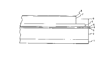
BRIEF DESCRIPTION OF THE DRAWINGS
Fig. 1 is a cross-sectional view of a multi-layer
photoreceptor of the invention.
Figs. 2-4 are test prints of printings provided by
electrophotographic imaging members.
220a239
DESCRIPTION OF PREFERRED EMBODIMENTS
The Supportinq Substrate
The supporting substrate 2 may be opaque or
substantially transparent and may comprise numerous
suitable materials having the required mechanical
properties. An aluminum drum is the preferred substrate.
The substrate may further be provided with an
electrically conductive surface (ground plane 3).
Accordingly, the substrate may comprise a layer of an
electrically non-conductive or conductive material such as
an inorganic or an organic composition. Various known
resins can be used as the electrically nonconducting
material, including polyesters, polycarbonates,
polyamides, polyurethanes, and the like. For a belt-type
imaging member, the electrically insulating or conductive
substrate should be flexible and may have any number of
different configurations such as, for example, a sheet, a
scroll, an endless flexible belt, and the like.
Preferably, the substrate is in the form of an endless
flexible belt and comprises a commercially available
biaxially oriented polyester known as Mylar, available
from E.I. du Pont de Nemours & Co., or Melinex available
from ICI Americas Inc.
The preferred thickness of the substrate layer
depends on numerous factors, including economic
considerations. The thickness of this layer may range
from about 65 micrometers to about 150 micrometers, and
preferably from about 75 micrometers to about 125
micrometers for optimum flexibility and minimum induced
surface bending stress when cycled around small diameter
rollers, e.g., 19 millimeter diameter rollers. The
substrate for a flexible belt may be of substantial
thickness, for example, 200 micrometers, or of minimum
thickness, for example, 200 micrometers, or of minimum
thickness, for example 50 micrometers, provided there are
no adverse effects on the final photoconductive device.
The surface of the substrate layer is preferably cleaned
prior to coating to promote greater adhesion of adjacent
2200239
layer. Cleaning may be effected by exposing the surface
of the substrate layer to plasma discharge, ion
bombardment and the like.
The ElectricallY Conductive Ground Plane
The electrically conductive ground plane 3 (if
needed) may be an electrically conductive layer such as a
metal layer which may be formed, for example, on the
substrate 2 by any suitable coating technique, such as a
vacuum depositing technique. Typical metals include
aluminum, zirconium, niobium, tantalum, vanadium, hafnium,
titanium, nickel, stainless steel, chromium, tungsten,
molybdenum, and the like, and mixtures and alloys thereof.
The conductive layer may vary in thickness over
substantially wide ranges depending on the optical
transparency and flexibility desired for the
electrophotoconductive member. Accordingly for a flexible
photoresponsive imaging device, the thickness of the
conductive layer is preferably between about 20 Angstroms
to about 750 Angstroms, and more preferably from about 50
Angstroms to about 200 Angstroms for an optimum
combination of electrical conductivity, flexibility and
light transmission.
Regardless of the technique employed to form a
metal layer, a thin layer of metal oxide generally forms
on the outer surface of most metals upon exposure to air.
Thus, when other layers overlying the metal layer are
characterized as "continuous" layers, it is intended that
these overlying contiguous layers may, in fact, contact a
thin metal oxide layer that has formed on the outer
surface of the oxidizable metal layer. Generally for rear
erase exposure, a conductive layer light transparency of
at least about 15 percent is desirable. The conductive
layer need not be limited to metals. Other examples of
conductive layers may be combinations of materials such as
conductive indium tin oxide as a transparent layer for
light having a wavelength between about 4000 Angstroms and
about 9000 Angstroms or a conductive carbon black
dispersed in a plastic binder as an opaque conductive
2200239
layer. The conductive ground plane 3 may be omitted if a
conductive substrate is used.
The Charge Blocking Layer
After deposition of any electrically conductive
ground plane layer, the charge blocking layer 4 may be
applied thereto. Electron blocking layers for positively
charged photoreceptors allow holes from the imaging
surface of the photoreceptor to migrate toward the
conductive layer. For negatively charged photoreceptors,
any suitable hole blocking layer capable of forming a
barrier to prevent hole injection from the conductive
layer to the opposite photoconductive layer may be
utilized.
The blocking layer 4 may include polymers such as
polyvinylbutyral, epoxy resins, polyesters, polysiloxanes,
polyamides, polyurethanes and the like; nitrogen-
containing siloxanes or nitrogen-containing titanium
compounds such as trimethoxysilyl propyl ethylene diamine,
beta-(aminoethyl) gamma-amino-propyl trimethoxy silane,
isopropyl aminobenzene sulfonyl titanate,
di(dodecylbenzene sulfonyl) titanate, isopropyl di(4-
aminobenzoyl)isostearoyl titanate, isopropyl
tri(methylamino) titanate, isopropyl trianthranil
titanate, isopropyl tri(N,N-dimethylethylamino) titanate,
titanium-4-amino benzene sulfonate oxyacetate, titanium 4-
aminobenzoate isostearate oxyacetate, [H2N(CH2-
)4]CH3Si(OCH3)2 (gamma-aminobutyl methyl dimethoxy
silane), [H2N(CH2)3]CH3Si(OCH3)2 (gamma-aminopropyl methyl
dimethoxy silane), and [H2N(CH2)3]Si(OCH3)3 (gamma-
aminopropyl trimethoxy silane) as disclosed in U.S.Patents Nos. 4,338,387, 4,286,033 and 4,291,110.
A preferred hole blocking layer comprises a
reaction product of a hydrolyzed silane or mixture of
hydrolyzed silanes and the oxidized surface of a metal
ground plane layer. The oxidized surface inherently forms
on the outer surface of most metal ground plane layers
when exposed to air after deposition. This combination
enhances electrical stability at low relative humidity.
2200239
The hydrolyzed silanes that can be used are hydrolyzed
silanes that are well known in the art. For example, see
U.S. Patent No. 5,091,278 to Teuscher et al.
The blocking layer 4 should be continuous and may
have a thickness of up to 2 micrometers depending on the
type of material used. A blocking layer of between about
0.005 micrometer and about 0.3 micrometer is satisfactory
because charge neutralization after the exposure step is
facilitated and good electrical performance is achieved.
A thickness between about 0.03 micrometer and about 0.06
micrometer is preferred for blocking layers for optimum
electrical behavior.
The blocking layer 4 may be applied by any
suitable technique such as spraying, dip coating, draw bar
coating, gravure coating, silk screening, air knife
coating, reverse roll coating, vacuum deposition, chemical
treatment and the like. For convenience in obtaining thin
layers, the blocking layer is preferably applied in the
form of a dilute solution, with the solvent being removed
after deposition of the coating by conventional techniques
such as by vacuum, heating and the like. Generally, a
weight ratio of blocking layer material and solvent of
between about 0.5: 100 to about 5.0: 100 is satisfactory
~ for spray coating.
The Adhesive Layer
An intermediate layer 5 between the blocking layer
and the charge generating or photogenerating layer may be
provided to promote adhesion. However in the present
invention, a dip coated aluminum drum is the preferred
substrate and is utilized without an adhesive layer. When
an adhesive layer is utilized, it can be characterized by
a dry thickness between about 0.01 micrometer to about 0.3
micrometer, more preferably about 0.05 to about 0.2
micrometer.
An adhesive layer, if utilized, may comprise any
known adhesive for layers of an electrophotographic
imaging member. The adhesive layer may comprise a film-
forming polyester resin adhesive such as du Pont 49,000
220023q
resin (available from E.I. du Pont de Nemours & Co.),
Vitel 1200 (available from Goodyear Rubber & Tire Co.), or
the like.
Both the duPont 49,000 and Vitel 1200 adhesive
layers provide reasonable adhesion strength and produce no
deleterious electrophotographic impact on the resulting
imaging member.
Another copolyester resin adhesive is available
from Goodyear Tire & Rubber Co. as Vitel 2200. This
polyester resin is a linear saturated copolyester of two
diacids and two diols. The molecular structure of this
linear saturated copelyester is represented by the
following:
HOC-(di;~ad-diol)n-OH
where the ratio of diacid to ethylene glycol in the
copelyester is 1: 1. The diacids are terephthalic acid and
isophthalic acid in a ratio of 1. 2: 1. The two diols are
ethylene glycol and 2,2-dimethyl propane diol in a ratio
of 1. 33: l . The Goodyear Vitel 2200 linear saturated
copelyester consists of randomly alternating monomer units
of the two diacids and the two diols and has a weight
average molecular weight of about 58,000 and a Tg of about
67?C .
Other suitable copolyesters include Goodyear Vitel
1710, Vitel 1870, Vitel 3300, Vitel 3550 and Vitel 5833.
Vitel 5833 is a short chained branched polymer having
cross-linkable hydroxyl and carboxylic acid functional
groups. Vitel 5833 is particularly useful by itself or
blended with other polyesters in applications requiring an
increase of adhesive layer cross-linking density.
The Charge Generating Layer
The charge generating layer 6 comprises a polymer
binder and a mixture of photoconductive pigments. The
220023q
photoconductive pigments are a mixture of hydroxygallium
phthalocyanine and alkoxygallium phthalocyanine dimer.
U.S. application Serial No. 08/169,486,
illustrates a process for the preparation of
hydroxygallium phthalocyanine Type V. The disclosure of
this Application is incorporated herein by reference. In
the Application, pigment precursor Type I chlorogaillium
phthalocynine is prepared by reaction of about 10 parts to
about 100, preferably about 19 parts, gallium chloride in
a solvent such as N-methylpyrrolidone, with
1,3diiminoisoindolene (DI3) in an amount of about 1 part
to about 10 parts, preferably about 4 parts, for each part
of gallium chloride. The resulting pigment precursor
chlorogaillium phthalocyanine is hydrolyzed by standard
methods. For example the pigment precursor can be
hydrolyzed by acid pasting, wherein the precursor is
dissolved in concentrated sulfuric acid and then
precipitated in a solvent, such as water, or from a dilute
ammonia solution, for example, from about 10 to about 15
percent ammonia. The resulting hydrolyzed hydroxygallium
phthalocyanine pigment is treated in a solvent, such as
N,N-dimethylformamide, present an amount of from about 1
volume part to about 50 volume parts and preferably about
volume parts for each weight of hydroxygallium
phthalocyanine. The pigment in solvent is treated by ball
milling in the presence of spherical glass beads,
approximately 1 millimeter to 5 millimeters in diameter,
at room temperature, about 25~C, for a period of from
about 1 hours to about 1 week, preferably for about 24
hours. The treatment produces a hydroxygallium
phthalocyanine Type V containing very low levels of
residual chlorine of from about 0.001 percent to about O.l
percent.
Additionally, processes for the preparation of
hydroxygallium phthalocyanine are illustrated in copending
patent applications U.S. Serial No. 08/413,554 and U.S.
Serial No. 08/332,304 and in U.S. Patents No. 5,456,998 to
Burt et al., No. 5,466,796 to Burt et al. and No.
2200239
5,493,016 to Burt et al. The disclosure~ of each
application and each U.S. Patent are incorporated herein
by reference.
Additionally, U.S. Patent No. 5,493,016 to Burt et
al., U.S. Patent No. 5,466,796 to Burt et al., U.S. Patent
No. 5,456,998 to Burt et al. and U.S. Patent No. 5,521,306
to Burt et al. disclose alkoxymetallo phthalocyanine
dimers and their preparations that are suitable in the
present invention. The disclosures of these references
are incorporated herein by reference. U.S. Patent No.
5,493,016 to Burt et al. teaches a process for the
preparation of alkoxy-bridged metallo-phthalocyanine
dimers by the reaction of a trivalent metal compound with
ortho-phthalodinitrile or 1,3-diiminoisoindolene in the
presence of a diol. U.S. Patent No. 5,466,796 teaches
alkoxy-bridged metallophthalocyanine C32Hl6N8MOROMN8Hl6C321
wherein M is a metal and R is an alkyl or an alkyl ether.
U.S. Patent No. 5,456,998 to Burt et al. teaches
photoconductive imaging members comprised of an alkoxy-
bridged metallophthalocyanine dimer as a charge generatormaterial, wherein the dimer is of the formula
C32Hl6N8MOROMN8Hl6C32, where M is a trivalent metal and R is
an alkyl group or an alkyl ether group. U.S. Patent No.
5,521,306 to Burt et al. teaches a process for preparation
of Type V hydroxygallium phthalocyanine, which comprises
in situ forming an alkoxy-bridged gallium phthalocyanine
dimer, hydrolyzing the alkoxy-bridged gallium
phthalocyanine dimer to hydroxy phthalocyanine and
converting the hydroxygallium phthalocyanine product to
Type V hydroxygallium phthalocyanine.
Suitable hydroxygallium phthalocyanines and
suitable alkoxygallium phthalocyanines are disclosed in
the Burt et al. patents identified above and in U.S.
Patent No. 5,521,306 to Burt et al. In particular, the
Burt et al. Application discloses alkoxygallium
phthalocyanine dimers of the general formula
C32Hl6N8GaOROGaN8Hl6C32 as illustrated by Formula 1:
- 2200239
FORMULA 1
N-
N N ~ G ~ - - - N
_~ N ¦ N
- N I [--
O
R
o
N-
N N~G .---- N
N N
N-- I \~
with, for example, from 2 to about 10, and preferably
about 2 to 6 carbon atom~ in the alkoxy-bridging unit (O-
R-O), wherein R is an alkyl group or an alkyl ether.
The charge generating layer is formed by coating
on a conductive substrate, a coating composition prepared
by dispersing the hydroxygallium phthalocyanine and
alkoxygallium phthalocyanine dimer of the present
invention in a solution of binder resin in an organic
solvent. The ratio of the hydroxygallium phthalocyanine
to alkoxygallium phthalocyanine dimer as the pigment
depends upon the fine tuning required for an application.
In general, weight ratios from 99:1 to 1:99 may be used.
Preferably, the ratio can be 80:20 to 20:80. Other
suitable ratios include 60:40 to 40:60 and 55:45 to 45:55.
A compounding ratio of the phthalocyanine mixture
to the binder resin generally ranges from 40/1 to 1/10,
and preferably from 10/1 to /1:4, by weight. If the ratio
of the phthalocyanine mixture is too high, the stability
2200239
of the coating composition tends to be reduced. If it is
too low, the sensitivity of the charge generating layer
tends to be reduced.
The solvents to be used in the coating
compositions are preferably selected from those incapable
of dissolving the lower layer, i.e., the layer on which
the charge generating layer is applied. Examples of the
organic solvents include alcohols, e.g., methanol,
ethanol, and isopropanol; ketones, e.g., acetone, methyl
ethyl ketone, and cyclohexanone; amides, e.g., N,N-
dimethylformamide and N,N-dimethylacetamide; dimethyl
sulfoxides; ethers, e.g., tetrahydrofuran, dioxane, and
ethylene glycol monomethyl ether; esters, e.g., methyl
acetate and ethyl acetate; halogenated aliphatic
hydrocarbons, e.g., chloroform, methylene chloride,
dichloroethylene, carbon tetrachloride, and
trichloroethylene; and aromatic hydrocarbons, e.g.,
benzene, toluene, xylene, ligroin, monochlorobenzene, and
dichlorobenzene.
The coating composition for a charge generating
layer can be applied by any known coating technique, such
as dip coating, spray coating, spin coating, bead coating,
wire bar coating, blade coating, roller coating, and
curtain coating. Drying after coating is preferably
carried out by first drying at room temperatures to the
touch and then heat-drying. Heat drying may be performed
at a temperature of from 20~ to 200~C for a period of from
5 minutes to 2 hours in still air or in an air flow. The
charge generating layer usually has a thickness of from
about 0.05 to 5 microns.
The Charge Transport Layer
The charge transport layer 7 may comprise any
suitable transparent organic polymer or non-polymeric
material capable of supporting the injection of
photogenerated holes or electrons from the charge
generating layer 6 and allowing the transport of these
holes or electrons to selectively discharge the surface
charge. The charge transport layer not only serves to
2200239
transport holes or electrons, but also protects the charge
generating layer from abrasion or chemical attack and
therefore extends the operating life of the imaging
member.
The charge transport layer is substantially
transparent to radiation in a region in which the imaging
member is to be used. The charge transport layer is
normally transparent when exposure is effected
therethrough to ensure that most of the incident radiation
is utilized by the underlying charge generating layer.
When used with a transparent substrate, imagewise exposure
or erase may be accomplished through the substrate with
all light passing through the substrate. In this case,
the charge transport material need not transmit light in
the wavelength region of use.
The charge transport layer may comprise activating
compounds dispersed in normally electrically inactive
polymeric materials for making these materials
electrically active. These compounds may be added to
polymeric materials that are incapable of supporting the
injection of photogenerated charge and incapable of
allowing the transport of this charge. An especially
preferred transport layer employed in multilayer
photoconductors comprises from about 25 percent to about
75 percent by weight of at least one charge transporting
aromatic amine compound, and about 75 percent to about 25
percent by weight of a polymeric film forming resin in
which the aromatic amine is soluble.
The charge transport layer is preferably formed
from a mixture comprising one or more compounds having the
general formula:
220023q
R1
\
N R3
/
R2
wherein Rl and R2 are selected from the group consisting
of substituted or unsubstituted phenyl groups, naphthyl
groups, and polyphenyl groups and R3 is selected from the
group consisting of substituted or unsubstituted aryl
groups, alkyl groups having from 1 to 18 carbon atoms and
cycloaliphatic groups having from 3 to 18 carbons atoms.
The substituents should be free from electron-withdrawing
groups such as NO2 groups, Cn groups, and the like.
Examples of charge transporting aromatic amines
represented by the structural formula above include
triphenylmethane, bis (4-diethylamine-2-methylphenyl) -
phenylmethane; 4, 4 ' -bis (diethylamino) 2, 2 ' -
dimethyltriphenylmethane ; N, N' -bis (alkyl-phenyl) - (1 ,1 ' -
biphenyl)4,4'-diamine wherein the alkyl is, for example
methyl, ethyl, propyl, n-butyl, etc ., N, N' -diphenyl-N, N' -
bis ( 3 -methylphenyl ) - ( 1, 1 ' -biphenyl ) - 4, 4 ' - diamine; and the
like, dispersed in an inactive resin binder.
Any suitable inactive resin binder soluble in
2 0 methylene chloride or other suitable solvent may be
employed. Typical inactive resin binders soluble in
methylene chloride include polycarbonate resin,
polyvinylcarbazole, polyester, polyacrylate, polyether,
polysulfone, and the like. Molecular weights can vary
from about 20, 000 to 1, 500, 000 . Other solvents that may
dissolve these binders include tetrahydrofuran, toluene,
trichloroethylene, 1, 1, 2-trichloroethane, 1, 1, 1-
trichloroethane, and the like.
The preferred electrically inactive resin
3 0 materials are polycarbonate resins having a molecular
weight from about 20, 000 to about 120, 000, more preferably
2200239
14
from about 50,000 to about 100,000. The materials most
preferred as the electrically inactive resin materials are
poly(4,4'-dipropylidene-diphenylene carbonate) with a
molecular weight of from about 35,000 to about 40,000,
available as Lexan 145 from General Electric Company;
poly(4,4'-isopropylidene-diphenylene carbonate) with a
molecular weight of from about 40,000 to about 45,000,
available as Lexan 141 from General Electric Company; a
polycarbonate resin having a molecular weight of from
about 50,000 to about 100,000, available as Makrolon from
Farbenfabricken Bayer A.G.; a polycarbonate resin having a
molecular weight of from about 20,000 to about 50,000,
available as Merion from Mobay Chemical Company; polyether
carbonates; and 4,4'-cyclohexylidene diphenyl
polycarbonate. Methylene chloride solvent is a desirable
component of the charge transport layer coating mixture
for adequate dissolving of all the components and for its
low boiling point.
The thickness of the charge transport layer may
range from about 10 micrometers to about 50 micrometers,
and preferably from about 15 micrometers to about 35
micrometers. Optimum thicknesses may range from about 23
micrometers to about 31 micrometers.
The Ground Strip
Ground strip 9 may comprise a film-forming binder
and electrically conductive particles. Cellulose may be
used to disperse the conductive particles. Any suitable
electrically conductive particles may be used in the
electrically conductive ground strip layer 9. The ground
strip 9 may comprise materials which include those
enumerated in U.S. Patent No. 4,664,995. Typical
electrically conductive particles include carbon black,
graphite, copper, silver, gold, nickel, tantalum,
chromium, zirconium, vanadium, niobium, indium tin oxide
and the like. The electrically conductive particles may
have any suitable shape. Typical shapes include
irregular, granular, spherical, elliptical, cubic, flake,
filament, and the like. Preferably, the electrically
2200239
conductive particles should have a particle size less than
the thickness of the electrically conductive ground strip
layer to avoid an electrically conductive ground strip
layer having an excessively irregular outer surface. An
average particle size of less than about 10 micrometers
generally avoids excessive protrusion of the electrically
conductive particles at the outer surface of the dried
ground strip layer and ensures relatively uniform
dispersion of the particles through the matrix of the
dried ground strip layer. Concentration of the conductive
particles to be used in the ground strip depends on
factors such as the conductivity of the specific
conductive particles utilized.
The ground strip layer may have a thickness from
about 7 micrometers to about 42 micrometers, and
preferably from about 14 micrometers to about 27
micrometers.
The Anti-Curl LaYer
The anti-curl layer 1 is optional, and may
comprise organic polymers or inorganic polymers that are
electrically insulating or slightly semi-conductive. The
anti-curl layer provides flatness and/or abrasion
resistance.
Anti-curl layer 1 may be formed at the back side
of the substrate 2, opposite to the imaging layers. The
anti-curl layer may comprise a filmforming resin and an
adhesion promoter polyester additive. Examples of film-
forming resins include polyacrylate, polystyrene,
poly(4,4'-isopropylidene diphenyl carbonate), 4,4'-
cyclohexylidene diphenyl polycarbonate, and the like.Typical adhesion promoters used as additives include
49,000 (du Pont), Vitel PE-100, Vitel PE-200, Vitel PE-307
(Goodyear), and the like. Usually from about 1 to about
15 weight percent adhesion promoter is selected for film-
forming resin addition. The thickness of the anti-curl
layer is about 3 micrometers to about 35 micrometers, and
preferably about 14 micrometers.
2200239
The anti-curl coating may be applied as a solution
prepared by dissolving the film forming resin and the
adhesion promoter in a solvent such as methylene chloride.
The solution is applied to the rear surface of the
supporting substrate (the side opposite to the imaging
layers) of the photoreceptor device by hand coating or by
other methods known in the art. The coating wet film is
then dried to produce the anti-curl layer 1.
The Overcoating Layer
The optional overcoating layer 8 may comprise
organic polymers or inorganic polymers that are capable of
transporting charge through the overcoat. The overcoating
layer may range in thickness from about 2 micrometers to
about 8 micrometers, and preferably from about 3
micrometers to about 6 micrometers. An optimum range of
thickness is from about 3 micrometers to about 5
micrometers.
The invention will further be illustrated in the
following, nonlimiting examples, it being understood that
these examples are intended to be illustrative only and
that the invention is not intended to be limited to the
materials, conditions, process parameters and the like
recited therein.
EXAMPLES
Table 1 lists various blend ratios of
hydroxygallium phthalocyanine and alkoxygallium
phthalocyanine dimer according to the invention. The
pigments were dispersed separately and then blended to the
desired ratio. The compositions were evaluated for PIDC
sensitivity. The sensitivities are reported in the Table.
In the Table, ROGaPc is alkylkoxygallium phthalocyanine
wherein R is -OCH2CH20- and HOGaPc is hydroxygallium
phthalocyanine.
2200239
Table 1
Device ROGaPc:HOGaPc dV/dX
No. ratio v cm2/erg
350VDDP
4238704 100:0 37
4256702 95:5 46
4256704 90:10 56
4249705 85:15 68
4249707 70:30 106
4249711 50:50 156
4256706 25:75 183
4256709 10:90 202
The following Table 2 shows dV/dX of a Hewlett
Packard Laserjet IIP printer, an AppleWriter Select 360
printer and a Hewlett Packard Laserjet 4 printer. These
three printers were selected because they represent
printers that require a low, medium and high sensitivity
photoreceptors. The fact that all three prints are
similar with regard to darkness demonstrates that the
sensitivity of the photoreceptor has been tuned over the~0 entire relevant range of sensitivities.
Table 2
Machine dV/dX
P-IIP 58
90:10 56
Apple LW 360 145
50:50 156
HP-4 224
10:90 blend 202
Figure 2 of the drawings shows a test print
generated in the Hewlett Packard printer. Figure 3 is a
test print generated in a Apple printer. Figure 4 is a
test print generated in the Hewlett Packard printer.
2200239
18
The print test results demonstrate that blending
mixtures of two pigments in accordance with the invention
permits tuning of photoreceptor compositions to provide a
range of sensitivities. The tuned photoreceptors are
capable of producing prints comparable to those made using
competitive photoreceptors.
The results shown in the Tables illustrate that
the present invention provides variable photosensitive
compositions. Proportions of hydroxygallium
phthalocyanine to alkoxygallium phthalocyanine can be
varied as dictated by the sensitivity requirements of a
range of applications. The present invention permits
compounding of a variety of products by use of only two
pigments.