Note: Descriptions are shown in the official language in which they were submitted.
2200219
- 1 -
FIELD EFFECT TRANSISTOR AMPLIFIER
BACKGROUND OF THE INVENTION
1. FIELD OF THE INVENTION
The present invention relates to an amplifier using a
field effect transistor (to be referred to as an FET
hereinafter) and, more particularly, to an FET amplifier
which is used as a low-noise amplifier for satellite
communication or the like and realizes noise reduction in a
wide band with a compact circuit.
2. DESCRIPTION OF THE PRIOR ART
In a low-noise amplifier for satellite communication,
a radio wave reaching from a satellite to the ground becomes
very weak because of attenuation in the radio wave propaga-
tion path between the satellite and the ground or a limita-
tion in transmission capability of the satellite itself.
For this reason, noise generated in the amplifier itself is
required to be minimized. In recent satellite communica-
tion, the frequency band used is broadening along with an
increase in traffic, and the amplifier must also cope with
a wide band. Therefore, the FET amplifier must have a
circuit arrangement capable of simultaneously meeting these
two requirements. Studies have been made to meet these
requirements by improving the input-side circuit of the FET
amplifier.
2200219
- 2 -
Generally, when a lossless matching circuit M1 is
connected to the input side of an FET 1, as shown in Fig. 1,
the noise figure of the FET 1 is determined by the source
admittance (Ys - Gs + jBs) of the input circuit, as repre
sented by the equation below:
F = Fo + Rn/Gs { ( Gs - Go ) z + ( Bs - Bo ) 2 }
F: noise figure defined by the input circuit
Fo: optimum noise figure
Rn: equivalent input noise resistance
Go: conductance giving optimum noise figure
Bo: susceptance giving optimum noise figure
Gs: conductance of the input circuit (source conduc-
tance)
Bs: the susceptance of the input circuit (source
susceptance)
To constitute a noise optimum FET amplifier on the
basis of this equation, it is preferable to make the source
admittance ( Ys - Gs + j Bs ) match the noise optimum admit-
tance (Yo = Go + jBo) defined by the FET. Reference symbol
M2 in Fig. 1 denotes an output matching circuit.
In the conventional FET amplifier, as shown in Fig. 2,
an output terminal 23 of an impedance improving isolator 2
having an input terminal 21 with transformers 24 to 26, a
dummy terminal 22, and an output terminal 23 terminated at
50 S2 is connected to the input terminal of the FET 1 through
2200279
- 3 -
a 7~/4 microstrip line 11 and an FET lead inductance 12,
thereby attaining matching for realizing optimum noise.
Reference numeral 13 denotes an output matching circuit. In
this circuit arrangement, however, a loss generated in the
matching circuit between the transformer 26 of the isolator
output portion and the ~,/4 microstrip line 11 degrades the
noise figure of the FET amplifier. The source impedance of
this amplifier exhibits a locus C in the Smith chart of
Fig. 3 when noise matching is achieved. However, the source
impedance for obtaining optimum noise is normally represent-
ed by a locus D in Fig. 3. The two loci have opposite
frequency directions and therefore cross each other. An
increase in noise at the band ends cannot be avoided, and
broad-band noise matching cannot be obtained.
To solve this crossing of the frequency loci after
noise matching, Japanese Unexamined Patent Publication
No. 63-62405 discloses a microwave amplifier having a
circuit arrangement for realizing noise reduction in a wide
band. This microwave amplifier has an FET 1 arranged on the
surface of a dielectric substrate with a ground conductor
formed on its surface and includes an input matching circuit
arranged between an input portion IN and the gate of the
FET 1, as shown in Fig. 4A. The input matching circuit 30
comprises an open-circuited stub 31 arranged at the input
25 portion, microstrip lines 32 and 33 for connecting the input
2200279
- 4 -
portion to the gate of the FET, and a short-circuited stub
34 arranged at a point on the microstrip line. Even when a
capacitor C is inserted between the ground and the distal
end of another microstrip line 35 instead of arranging the
short-circuited stub 34, a short end circuit can be real-
ized, as shown in Fig. 4B.
The change in input impedance locus of the amplifier
disclosed in this prior art will be described. The reflec-
tion coefficient from the gate of the FET to the input side
of the input matching circuit 30 is represented by rs, and
the reflection coefficients from the respective elements of
the input matching circuit 30 to the input side are repre-
sented by rl, rz, and r3. The electrical length of the
open-circuited stub 31, the microstrip lines 32 and 33, and
the short-circuited stub 34 is optimized so that the
reflection coefficients rl to r3 and rs change along loci 41
to 44 on the Smith chart of Fig. 5, respectively. The
reflection coefficient r2 which has changed along the locus
42 in the open-circuited stub 31 and the microstrip line 32
changes to the reflection coefficient r3 along the locus 43
in the short-circuited stub 34. The locus r3 is converted
into rs (44) by phase rotation along the microstrip line and
33 and overlaps an optimum input load reflection coefficient
roPt ( 45 ) of the FET. Normally, phase rotation of a micro-
strip line becomes larger as the frequency becomes higher.
2200279
- 5 -
For this reason, when the locus r3 reaches the position of
the locus rs, the length of the locus is small. However,
since the displacement from ropt (45) to rs (44) can be
reduced as compared to the arrangement shown in Fig. 2, the
arrangement shown in Fig. 4A or 4B can realize noise
matching in a wide band.
In a low-noise amplifier for satellite communication,
to apply the amplifier to the reception system without
degrading the characteristics of the amplifier even when the
input impedance condition changes in a device arrangement
including an amplifier input feed unit and an antenna, an
isolator is normally inserted to ensure the input impedance.
When the circuit shown in Fig. 4A or 4B is applied for
satellite communication, a 50-S2 matched three-terminal
isolator is connected to the input side. Therefore, the
noise figure drops by the loss of the isolator.
In the improved amplifier shown in Fig. 4A or 4B,
broadening of the noise figure in terms of frequency can be
attained to some extent, though the noise figure as an
absolute value is poor. When a 50-S2 matched isolator is
added to the prior art, the noise figure suffers by the loss
of the isolator. The reason for this is as follows. Since
a plurality of devices (open-circuited and short-circuited
stubs) associated with input broad-band matching and
microstrip lines are formed on the dielectric substrate,
2200279
- 6 -
noise degradation is caused by an increase in insertion
loss. The scale of the circuit including the input matching
circuit becomes large, hampering a size reduction of the
device. This is because the input matching circuit is
constituted and realized by microstrip lines as a distribut-
ed parameter circuit. As the frequency becomes lower, the
electrical length becomes larger, and the scale of the
circuit on the substrate also tends to be larger.
SUMMARY OF THE INVENTION
The present invention has been made in consideration of
the above situation, and has as its object to provide a
field effect transistor amplifier which realizes a
broad-band low-noise amplifier using an FET with a compact
and lossless input circuit arrangement to improve the
characteristics of the FET amplifier and also reduces the
size of the device.
In order to achieve the above object, according to the
basic aspect of the present invention, there is provided a
field effect transistor amplifier comprising a coaxial
dielectric resonance device inserted between an input
terminal of the amplifier and an input terminal of an FET
and having a ~./2 electrical length and a characteristic
impedance lower than an input-side impedance from the input
terminal of the amplifier to the input terminal of the FET.
The coaxial dielectric resonance device having the ~./2
2200279
electrical length comprises a TEM mode dielectric resonator
consisting of a high dielectric formed into a cylindrical
shape with a predetermined axial length, an outer conductor
formed by metallizing an outer surface of the dielectric
with a conductive material, and an inner conductor formed by
metallizing an inner wall of the dielectric with a conduc-
tive material. The coaxial dielectric resonance device
having the ~./2 electrical length has an inner conductor
exposed to one end connected to the input terminal side of
the amplifier and the internal conductor exposed to the
other end connected to the input terminal side of the FET.
In the present invention, preferably, an isolator
consisting of a three-terminal circulator with a terminated
one end is arranged on the input side of the amplifier, and
a ferrite end face of the central conductor the isolator is
connected to the coaxial dielectric resonance device having
the ~./2 electrical length as an output terminal. In
addition, preferably, an input-side lead inductance is
connected to the input terminal of the amplification device.
As described above, when a ~,/2 line constituted by a
low-loss and compact coaxial dielectric resonance device is
connected to the input terminal of the FET, and the charac-
teristic impedance of this ~,/2 line is made lower than the
impedance from the input terminal of the amplifier to the
input terminal of the amplification device, the ~,/2 line
2200279
_8-
generates series resonance. The high-frequency impedance of
the input-end impedance extends in the direction of capaci-
tance in terms of admittance, and the low-frequency extends
in the direction of permittivity in terms of admittance.
Assume that this extended impedance locus is rotated by the
FET input-side lead inductance of the FET in the direction
of permittivity on a Smith chart. Even if rotation by the
permittivity becomes larger as the frequency becomes higher
in impedance conversion by the FET input-side lead induc-
tance, the impedance originally has a locus on the Smith
chart (impedance chart) by series resonance of the ~/2 line
in which the high-frequency impedance extends to the lower
side, and the low-frequency impedance extends to the upper
side. Therefore, input noise matching is performed so that
the optimum noise locus and frequency direction do not
change, and a similar form of extension of the locus is
obtained while maintaining the form of extension (relative
positional relationship between the high-frequency impedance
and the low-frequency impedance) of the locus after imped-
ance conversion by the FET lead inductance.
The loss of the input portion will be considered. The
loss in impedance conversion of the isolator can be elimi-
nated by omitting the 50-~ matched input isolator output
portion. The loss of the input matching portion can be
reduced by constituting the ~/2 line by a small and high-Q
2200279
_ g _
coaxial dielectric resonance device. With the above
arrangement, a lossless input matching circuit can be
formed. Therefore, noise reduction in the entire band can
be achieved by minimizing the loss of the input circuit
while realizing broad-band noise matching.
In the present invention, the number of necessary main
devices associated with input broad-band matching is de-
creased, and the main device (~,/2 coaxial dielectric
resonance device) is made small. This arrangement contrib-
utes to size reduction of the device and also facilitates
assembly. The reason for this is as follows. When a
coaxial line formed by removing conductors on both sides of
the TEM mode coaxial dielectric resonance device serving as
a ~,/2 coaxial transmission line is manufactured using a
material with a high Q and high permittivity, the effective
coaxial length and diameter can be reduced.
In addition, according to the present invention, the
shield characteristics of the input matching circuit can be
improved. Therefore, an adverse effect of an external
interference wave or feedback oscillation can be prevented
and the circuit can be stably operated. This is because the
~./2 line serving as an input matching circuit is constituted
by the coaxial dielectric substrate device, and the conduc-
for in the transmission line is shielded by metallizing the
outer surface.
CA 02200279 1999-02-22
- 9a -
In accordance with the present invention there is
provided a field effect transistor amplifier using a field
effect transistor as an amplification device, comprising:
an amplifier unit; and a coaxial dielectric resonance device
inserted between an input terminal of said amplifier unit and
an input terminal of said field effect transistor and having a
~./2 electrical length and a characteristic impedance lower
than an input-side impedance from said input terminal of said
amplifier unit to said input terminal of said field effect
transistor.
74640-11
2200219
- 10 -
The above and many other advantages, features and
additional objects of the present invention will become
manifest to those versed in the art upon making reference to
the following detailed description and accompanying drawings
in which preferred embodiments incorporating the principles
of the present invention are shown by way of illustrative
example.
BRIEF DESCRIPTION
OF THE DRAWINGS
Fig. 1 is a block diagram showing the arrangement of
a
prior art;
Fig. 2 is a block diagram showing the detailed arrange-
ment of anothe r prior art;
Fig. 3 is a Smith chart for explaining the operation
of
the prior art shown in Fig. 2;
Figs. 4A and 4B are block diagrams showing the
arrangement of the
improved input
matching circuit
of the
prior art and a modification thereof, respectively;
Fig. 5 is a Smith chart for explaining the operation
of
the prior art shown in Fig. 4A or 4B;
Fig. 6 is a block diagram showing the arrangement of
an
embodiment of the present invention;
Figs. 7A to 7C are perspective and sectional views,
respectively, showing the ~,/2 line of the present invention;
Fig. 8 is a Smith chart for explaining the operation
of
the embodiment shown in Fig. 6;
2200279
- 11 -
Fig. 9 is a Smith chart for explaining a change in
locus of the characteristic impedance of the ~,/2 line in the
embodiment shown in Fig. 6;
Fig. 10 is a block diagram showing the arrangement of
another embodiment of the present invention; and
Fig. 11 is a graph showing the effect of the present
invention compared with the prior arts.
DETAILED DESCRIPTION OF THE PREFERRED EMBODIMENTS
Preferred embodiments of the present invention will be
described below with reference to the accompanying drawings.
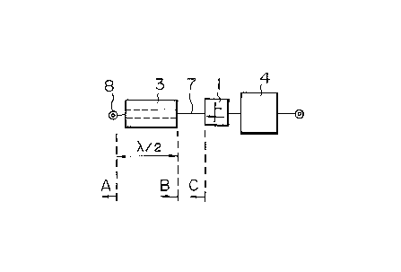
Fig. 6 is a block diagram showing the arrangement of the
first embodiment of the present invention. Referring to
Fig. 6, reference numeral 1 denotes a field effect transis-
for (FET) as an amplification device. An isolator 2 and a
~./2 coaxial line 3 are connected to the input side of the
FET 1, and an output matching circuit 4 is connected to the
output side of the FET 1. The isolator 2 is constituted by
a generally known three-terminal strip line circulator.
Reference numeral 2a denotes an input terminal formed by a
strip line; 2b, a dummy connection terminal having the same
structure as that of the input terminal 2a and connected to
a dummy terminal 5; and 2c, an output terminal directly
connected from the strip line on the ferrite end face to the
load side. A ferrite 6 is arranged at the center of the
isolator 2 while interposing a conductor.
2200279
- 12 -
The output terminal 2c of the isolator with the above
structure is directly soldered to the central conductor on
one end side of the coaxial dielectric resonance device 3
having a ~./2 electrical length and a characteristic imped-
ance lower than the output impedance (defined as an input
terminal) of the ferrite end, thereby constituting a
microwave circuit. As shown in the perspective views of
Figs. 7A and 7B and the sectional view of Fig. 7C, the
coaxial dielectric resonance device 3 having the ~,/2
electrical length is formed as follows. A dielectric
material having a high Q and high permittivity is formed
into a parallelepiped or circular cylinder 3a having a
predetermined axial length. The outer surface is metallized
with a conductive material to form an outer conductor 3b.
An axial cavity is formed at the central portion of the end
face of the dielectric device, and the inner wall is
metallized with a conductive material to form an inner
conductor 3c, thereby constituting a TEM mode dielectric
resonator. The conductive surfaces at the two ends are
removed to form open ends, so that a coaxial transmission
line is constituted. An FET lead inductance 7 is soldered
to the central conductor on the other end side of the ~./2
coaxial dielectric resonance device 3 and connected to the
FET 1.
According to the FET amplifier having the above
2200279
- 13 -
structure, an input signal supplied to the input terminal 2a
of the isolator 2 is supplied from the output terminal 2c to
the FET 1 through the ~,/2 coaxial dielectric resonance
device 3 and the FET lead inductance 7. A reflection wave
generated at the input terminal of the FET 1 enters the
isolator 2 again and is consumed by the dummy terminal 5
through the dummy connection terminal 2b. The signal
amplified by the FET 1 is supplied to a load through the
output matching circuit 4. By adjusting the characteristic
impedance value of the ~,/2 coaxial dielectric resonance
device 3, the input circuit of the FET 1 can be set to a
source impedance for obtaining optimum noise. The variable
range of the characteristic impedance value of the ~,/2
coaxial dielectric resonance device 3 is set to be narrower
than that of the output impedance of the ferrite end 2c of
the isolator.
The operation of the FET amplifier will be described
below in detail with reference to the Smith chart in Fig. 8.
Referring to Fig. 8, a locus A represents the impedance at
a point A of the output terminal of the isolator 2 obtained
in the embodiment shown in Fig. 6 in a wide frequency band.
A locus B represents the impedance at a point B of the
output terminal of the ~/2 coaxial dielectric resonance
device 3. The locus B is obtained by rotating the locus A
by ~./2 (one revolution) in terms of phase on the Smith chart
2200279
- 14 -
by the characteristic impedance of the ~./2 coaxial dielec-
tric resonance device 3. When the locus returns to the
original position, the high frequency extends to the lower
side, and the low frequency extends to the upper side,
unlike the locus A. This equals the series resonance effect
by the ~,/2 coaxial dielectric resonance device 3.
A locus C represents the source impedance at a point C
of the input terminal of the FET 1. The locus C is obtained
by rotating the locus B in the dielectric direction on the
chart by the FET lead inductance 7. In impedance conversion
by the FET lead inductance 7, the inductance rotation by the
permittivity becomes larger as the frequency becomes higher.
However, since the locus B already sufficiently extends to
the high-frequency and low-frequency directions due to the
series resonance effect of the ~./2 coaxial dielectric
resonance device 3, the frequency direction of the locus C
becomes eventually equal to that at the position of an
optimum noise locus D, and a similar form of extension of
the locus is obtained, though the extension of the locus by
the FET lead inductance 7 is reduced from the locus B to the
locus C.
As an adjustment device for the source impedance locus
C, a device is prepared by changing the characteristic
impedance of the ~,/2 coaxial dielectric resonance device 3,
i.e., the ratio of the outer diameter to the inner diameter
2200279
- 15 -
of the coaxial device. The locus C changes as shown in
Fig. 9. By using this effect, the locus can be matched with
the optimum noise locus. In Fig. 9, reference symbol Z
represents the characteristic impedance of the ~./2 line.
In the circuit arrangement of this embodiment, the loss
in impedance conversion of the isolator is eliminated by
omitting the 50-S2 matched input isolator output portion, and
the loss of the input matching portion is reduced by
constituting a ~,/2 coaxial line by a compact and high-Q
dielectric resonance device. With this arrangement, a
decrease in loss of each device can be realized while
minimizing the number of necessary main devices associated
with input broad-band matching as compared to the prior art.
Therefore, the degradation in noise figure as an absolute
value can be minimized, and broad-band noise matching can be
realized.
The second embodiment of the present invention will be
described below with reference to Fig. 10. Referring to
Fig. 10, the input terminal is connected to an input-side
load and already has an actual resistance component (e. g.,
50 S2) as an arbitrary input-side impedance. Reference
numeral 1 denotes a field effect transistor (FET); 8, an
input terminal; 7, an FET lead inductance; 3, a ~,/2 coaxial
line using a dielectric resonance device; and 4, an output
matching circuit. The input terminal 8 is soldered to the
' 2200279
- 16 -
central conductor on one end side of the coaxial dielectric
resonance device 3 having a ~,/2 electrical length and a
characteristic impedance lower than the impedance on the
input side. In addition, the FET lead inductance 7 is
soldered to the central conductor at the other end of the
~,/2 coaxial dielectric resonance device 3, and the FET 1 is
connected to the FET lead inductance 7. The coaxial
dielectric resonance device 3 having the ~,/2 electrical
length is the same as in the first embodiment. The flow of
an input signal is also the same as that after the isolator
ferrite terminal in the first embodiment.
The input terminal of the second embodiment is directly
constituted by, e.g., a waveguide transducer. By using the
difference in field strength distribution in the waveguide,
which changes depending on the insertion position of the
50-S2 line as the input terminal of the waveguide, the actual
resistance value as an arbitrary input-side impedance can be
realized.
As described above, in the amplifier according to the
first or second embodiment, the input circuit loss is
minimized while broad-band noise matching is realized. With
this arrangement, noise as an absolute value can be reduced
in the entire band. Fig. 11 is a graph showing the
noise-to-temperature characteristics. A curve a represents
the characteristics of the present invention; a curve b, the
2200279
characteristics of the prior art shown in Fig. 2; and a
curve c, the characteristics of the improved prior art shown
in Fig. 4A or 4B. In the amplifier according to the first
or second embodiment, the number of necessary devices
associated with input broad-band matching is reduced, and
the ~,/2 coaxial dielectric resonance device is made small.
Therefore, a size reduction of the device is enabled, and
assembly is facilitated. Additionally, the shield charac-
teristics of the input matching circuit portion are im-
proved. Since an adverse effect of an external interference
wave or feedback oscillation is prevented, the circuit can
be stably operated.