Note: Descriptions are shown in the official language in which they were submitted.
RCA 88,153
A METHOD FOR MANUFACTURING AN IMPREGNATED CATHODE
The present invention relates to a method for manufacturing
impregnated cathodes, especially for equipping electron guns for
- 5 cathode ray tubes.
An impregnated cathode contains a porous emitting plate of
refractory material (tungsten, molybdenum, rhenium, etc.)
impregnated with emitting material (barium, strontium, calcium,
aluminum, cesium, etc.). This plate is arranged on a support
10 generally in the form of a small refractory metal dish (tantalum,
molybdenum, etc.). The plate and dish unit forms the upper part
of the cathode.
The emitting plate and its support are assembled so as to
form a- mechanical unit capable of standing up under the various
15 phases of manufacture of the cathode and the high operating
temperatures of the cathode. Morever, the contact between the
plate and its support should be as good as possible in order to
guarantee the performance of the cathode.
Various methods have been used to make the upper part of
2 0 an impregnated cathode. One method consists of depositing a
coating on the back surface of the emitting plate to facilitate
soldering with the support. The coating is, in general, based on
powders of molybdenum and rhenium. The major disadvantages
are the high price of this coating; difficulty in storing due to high
2 5 degrees of evaporation and sedimentation; difficulty in controlling
and reproducing the quantity deposited on the support, which
causes a variable thickness of the interface; the impossibility of
depositing on small size cathodes (less than 2 mm); and the
required alignment of the surface of the plate covered with
30 coating to make the weld.
A second method, as indicated in U.S. Patent No. 5,218,263,
issued to L. R. Falce et al. on June 8, 1993, consists of mechanically
blocking the emitting plate of the cathode on the support by a cap
or a piece covering the latter in part. The cap has an opening to
35 permit the emission of the plate into the tube. This cap is
soldered with the support and thus forms a single piece with the
2 RCA 88,153
upper part of the cathode. The major disadvantages are an
increase of the weight of the cathode in making this structure,
which is to the detriment of the arcing time of the cathode; low
efficiency thermal conduction from the plate to the rest of the
5 cathode, to the detriment of the overall performance of the
cathode; a risk of assembling the plate at a bias or with a high
degree of freedom; the presence of a metal piece between the
electrode of the gun situated in front of the cathode and the
surface of the plate, which piece modifies the conformation of the
10 applied electrical field; and a subsequent deposit of the material
on the surface of the plate at the outlet of the cathode that lowers
the output from the cathode.
A third method, divulged in U.S. Patent No. 5,171,180, issued
to K. S. Lee on December 15, 1992, consists of directly assembling
15 the plate onto its support without soldering, then treating the
assemby of parts in a high temperature hydrogen furnace to cause
a chemical reaction of the emitting products contained in the plate
with the support, in order to make a bond. The major
disadvantages are the loss of emitting materials contained in the
20 plate, to be able to make the bond with the support, which
reduces the service life of the cathode; the treatment in a
hydrogen furnace, necessitating having only one pile of many
small size parts; the correct positioning of the plate not being
guaranteed during the handling in the furnace or by the
2 5 movements caused to the plate in its positioning during the
chemical reaction; a positioning stability not being guaranteed for
the plate during the use; and the possibility of delamination of the
products .
A fourth method, divulged by U.S. Patent No. 5,128,584,
30 issued to J. Choi on July 7, 1992, consists of soldering the cathode
plate directly with its support, with a preliminary treatment
roughening the two surfaces to be joined. The soldering is carried
out by electrical resistance and is facilitated by the good contact
made between the two components. The greatest disadvantages
3 5 are the power necessary for soldering the refractory material,
which causes a high increase in temperature modifying or
~ ~ n ~ ~ 3
3 RCA 88,153
destroying in part the emission products contained in the plate;
the fragility of the solder, because the latter remains weak and
fragile during the assembly of the cathodes into the electron gun;
the obligation to align the face of the plate made rough to make
5 the solder; and the difficulty of aligning the surface of a plate of
small size (less than 2 mm).
Thus, there is need for a procedure for manufacturing an
impregnated cathode and, more particularly, a procedure for
assembling the emitting plate to its support, which does not have
10 the disadvantages of the state of the art, which is simple to put
into operation and economical, and whose effects are neutral,
relative to the emissivity of the plate, while guaranteeing a
reliable and repeatable positioning of the plate onto its support.
A method of manufacturing an impregnated cathode,
15 according to the invention, includes soldering a porous emitting
plate of refractory material inside a support of refractory metal,
wherein, to facilitate the soldering, a purely metallic transport
material is arranged between the emitting plate and its support.
In a particularly advantageous form of implementation, the
20 transport material is a thin metal tab inserted between the
emitting plate and its support.
In the drawings:
Figure 1 is a cut-away side view of an impregnated cathode
according to the state of the art;
Figure 2 is a side view of a cathode, in accordance with the
present invention, showing the upper part of the cathode in
exploded view; and
Figure 3 is a top view, and Figure 4 is a cut-away side view,
illustrating a preferential mode of implementation of the present
30 invention.
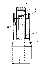
As indicated in Figure 1, an impregnated cathode generally
includes a cylindrical body 2 at the end of which is an upper part
of the cathode consisting of an emitting plate 1, most often
containing tungsten as a basic material, arranged on a support 13,
3 5 most often of tantalum or molybdenum. Inside the body 2 is
inserted a heating element 5. A cylinder 4 forms the outer skirt
4 RCA 88,153
of the cathode and serves as a heat shield to prevent losses of the
heat created by the heating element 5, thus increasing the thermal
efficiency of the assembly. The body of the cathode 2 is kept in
position inside the shield by strips 3 soldered to the body 2 (e.g.,
5 at points 6, as shown in Figure 2) and to the outer skirt 4.
One of the difficulties concerning the assembly of the
various elements of the cathode involves the connection of the
plate 1 to its support 13. This connection should be mechanically
strong, offer an excellent thermal transmission, and be neutral
10 toward the emission properties of the plate, all at high operating
temperatures which may exceed 1200~C.
The parameters of stability during emission, service life,
arcing time, and stability of the emission threshold depend
essentially on the mechanical strength of the plate with the rest of
15 the cathode structure.
Because the emitting plate and its support are of refractory
materials, it is extremely difficult to make, by soldering, the direct
connection of the two components. The numerous solutions
divulged in the state of the art do not offer a simple, reliable, and
2 0 cheap solution with the characteristics of repeatability necessary
for mass producing a key component of cathode ray tubes.
To obtain a superior contact between the refractory metal
support 13 and the emitting plate 1, which contact makes it
possible to optimize the thermal conduction between the heating
25 element 5 and the plate, it is necessary to join by soldering the
materials together without destroying the porosity of the plate
and without modifying the emission characteristics, which
prohibits a soldering at a temperature which is too high.
As indicated in Figure 2, the invention proposes inserting
30 between the emitting plate 1 and its support 13, a metal transport
material 8, which is chemically neutral and which permits
soldering the two components at a sufficiently low temperature so
as not to deteriorate the emission characteristics of the plate. For
this, the material chosen should have a melting point between the
3 5 operating temperature of the cathode and that of the metals
constituting the plate.
RCA 88,153
The transport material, placed as an interface between the
plate and its support, may be in the form of metal powder, flat
ribbon, or wire.
Because it is necessary to minimi7e the amount of transport
5 material, in order to reduce the weight and/or size of the cathode
particularly for heat output reasons, the transport material may,
in one advantageous mode of implementation, be deposited by
vaporization in a vacuum directly upon the support 13. In this
way, the thickness of the layer of material 8 may be controlled,
10 preferably to between 1 and 25 microns, a thickness permitting
good solderability of the components 1 and 13 without affecting
the heat output characteristics of the cathode.
In another preferential mode of implementation, the
transport material is in the form of a thin metal tab with a
15 thickness chosen between 1 and 25 microns. Advantageously, the
tab is cut so as not to occupy the whole contact surface between
the support 13 and the plate 1, in order to reduce the weight of
the transport material. To reliably perform the soldering between
the plate and its support, it is necessary, however, that the surface
20 covered by the transport material be sufficient, taking into
account the small dimensions of the components to be soldered.
Experience has shown that a tab surface area ranging between 0.4
and 0.7 times the surface area of the face of the plate, generally of
a rounded shape, would make it possible to ensure the soldering
2 5 of the components under good conditions of reliability.
As illustrated in Figure 3, showing a view of the inside of the
support 13, the tab 10 is, for example, cut in the form of a
rectangle with rounded corners, which shape has the advantage of
automatic centering during its insertion into the support 13,
30 generally in the form of a dish. In this way, there is moreover
ensured the soldering of the plate 1 to its support 13 by situating
the soldering points 9 in the center part of the plate. For a
circularly cylindrical emitting plate with a diameter of 1.27 mm,
there is chosen, by way of example, a metal tab 1.1 mm long by
35 0.6 mm wide with a metal thickness which can be selected from l
to 25 microns.
5 ~ ~
6 RCA 88,153
The metal of the interface material 8 should be chosen so as
not to have a chemical reaction at high temperature, while making
it possible to ensure a good mechanical connection between the
plate and its support. Likewise, its melting point should be
S sufficiently low so as not to reduce the emissivity characteristics
of the plate.
Various metals may be used, whether pure or in the form of
alloys, to implement the invention: nickel, chromium, vanadium,
and rhenium, for example, have given excellent results, both from
10 a mechanical standpoint, as well as from a standpoint of neutrality
toward the emissivity properties of the emitting plate.
In one advantageous mode of implementation, pure nickel
was selected to make the tab 10. This metal has a melting point of
1453~C, between the operating temperature of the cathode,
l S around 1200~C, and the melting point of the tungsten plate, of the
order of 3410~C; and it exhibits a good thermal conductivity and a
very good solderability with tungsten and tantalum. Moreover,
nickel offers the additional advantage of being a magnetic
material; thus, it permits considering an automated deposit by
20 electromagnet of the tab on the dish, which deposit would be very
difficult manually, taking into account the small dimensions of the
- components constituting the cathode.