Note: Descriptions are shown in the official language in which they were submitted.
CA 02200675 1997-03-21
-1_
FIELD OF INVENTION
The invention relates generally to the field of antennas and more
particularly to printed antennas, namely antennas composed of thin layers of
electrically conductive material bonded onto a thin, planar, dielectric
material.
BACKGROUND OF THE INVENTION
With the advent of mobile clap top" computers, there has been an
increased demand to link such devices in a wireless local area network.
Likewise, there has been a marked increase in the use of wireless devices
such as miniature cordless phones and pagers. A general problem in the
design of laptops and other types of small, portable, wireless data
communication products lies in the type of radiating structure required for
the unit, which should be convenient and reliable. When an external dipole
or monopole structure is used, such an antenna can be readily broken in
normal use. Also, the cost of the external antenna and its associated
conductors add considerably to the cost of the final product.
In an effort to avoid use of an external antenna, some manufacturers
have used conventional microstrip patch antennas, the characteristics of
which are well known. Basically, a microstrip patch antenna comprises a
dielectric material, such as a printed circuit board, which has two opposed
I:~IPG7\AP0~.51636\OOIOS~PATENT3.DOC
CA 02200675 1997-03-21
~2~A67
-2-
surfaces. One of the surfaces is coated with an electrically conductive layer
which functions as a ground plane, and the other opposed surface has an
essentially rectangularly or circularly shaped electrically conductive layer
("microstrip patch") disposed so as to extend over the ground plane. This
structure provides the main radiating element of the microstrip patch
antenna. In the rectangular patch antenna, the rectangular patch has a
length equal to substantially one-half the wavelength of the resonant
frequency, also called the resonant wavelength. In the circular patch
antenna, the circular patch has a diameter of about 0.6 of the resonant
wavelength. Either type of microstrip patch antenna presents a thin
resonating cavity wherein a standing electromagnetic wave can exist in the
patch and wherein radiation emanates from the edges thereof.
Microstrip patch antennas, however, have many limitations. One
limitation is that the microstrip patch antenna can only typically radiate
above the ground plane, which is a necessary element of the device. The
need for a ground plane also causes the resonant frequency of the antenna
to depend on the dielectric constant of the printed circuit board, which can
vary considerably due to manufacturing variances. Thus it is difficult to
mass produce tuned devices of this kind. Moreover, because the microstrip
patch antenna is a highly resonant thin cavity structure, the bandwidth of
such an antenna is greatly dependent upon the thickness of the dielectric
I:\IPG7\APO\51636\00105\PATENT'3.DOC
CA 02200675 1997-03-21
-3-
material. Thus, very thin printed circuit boards, which are increasingly
found in portable wireless communications devices, tend to limit the
available bandwidth provided with such antennas. Finally, the length of the
microstrip patch antenna is relatively large due to the necessity of having an
S overall length of about one-half the wavelength of the resonant frequency or
about 0.6 of such wavelength in the case of a circular microstrip patch
antenna. There are methods known in the art for increasing the bandwidth
and reducing the size of the microstrip patch antenna, but such method are
relatively complicated and generally not conducive to mass produced
devices.
The present invention seeks to overcome the limitations of prior art
printed antenna structures and allow for more robust radiating
characteristics while being more tolerant of manufacturing variances
typically encountered in mass produced printed circuit boards. It also
desired for the printed antenna to occupy relatively little area on the
printed
circuit board or other dielectric material.
SUMMARY OF THE INVENTION
According to one broad aspect of the invention, a printed antenna is
provided for transmission of a spectrum of electromagnetic waves having a
center wavelength ~o. The printed antenna comprises a thin dielectric
I:~IPG7~AP0~51636100105~PATENT'3.DOC
CA 02200675 1997-03-21
-4-
material having opposed surfaces. A strip of electrically conductive material
covers a portion of one of the surfaces of the dielectric material so as to
provide a radiating element. The strip of electrically conductive material,
however, does not substantially extend over any large regions of electrically
conductive material, such as a ground plane, disposed on the opposed
surface of the dielectric material. The strip of electrically conductive
material has an overall length of approximately Ao/2, and includes a first
segment and a sequential second segment which collectively compose a
main radiating element. The first and second segments are generally linear
in shape and disposed so as to be angled with respect to one another. A
transmission means, attached to the dielectric material, is provided for
coupling radio frequency energy between the radiating element of the
antenna and antenna driving circuitry.
In the preferred embodiment of this aspect of the invention according
to this first broad aspect thereof, the main radiating element substantially
assumes a "V"-shape wherein the linear segments thereof are orthogonal to
one another. The overall shape of the radiating element (which comprises
the main radiating element and the remaining portions of the strip of
electrically conductive material) resembles a hook composed of a
sequentially connected series of substantially linear segments.
I:~IPG71AP0151636~OOlOS~PATENT3.DOC
CA 02200675 1997-03-21
-5-
According to another broad aspect of the invention, a printed antenna
structure is provided which includes a dielectric material having opposed
surfaces. A first layer of electrically conductive material covers a
relatively
wide portion of one the surfaces of the dielectric material in order to
provide
a ground plane. A first strip of electrically conductive material covers a
portion of the opposite surface of the dielectric material and is disposed so
as to extend over the electrically conductive ground plane layer, so as to
provide a microstrip feed line. A second strip of electrically conductive
material provides a main radiating element for the antenna. It is electrically
connected to the first strip of conductive material, covering a portion of one
of the surfaces of the dielectric material and being disposed thereon so as to
not substantially extend over the electrically conductive ground plane layer.
The main radiating element includes sequential first and second segments
which are generally linear and disposed so as to be angled with respect to
one another.
In the preferred embodiment of this second broad aspect of the
invention, the printed antenna structure includes a third strip of
electrically
conductive material which provides a secondary radiating element. The third
strip has a fixed end continuous with the second strip of electrically
conductive material and a free terminal end that does not connect with the
second strip of electrically conductive material. The third strip is also
I:\IPG71AP0\51636\00105\PATENT3.DOC
CA 02200675 1997-03-21
-6-
disposed so as not to substantially extend over the ground plane layer, and
this strip includes third and fourth sequential, generally linear segments
which are angled with respect to one another. In the preferred embodiment,
the third and fourth segments are arranged so as to give the printed antenna
structure an overall shape which resembles a hook.
As described in greater detail below, the printed antenna of the
invention presents an omnidirectional radiation pattern having good coupling
characteristics over a wide spatial region. The antenna thus provides good
performance in a multi-path environment, where the angle of incidence of
the electric field of an incoming electromagnetic wave is substantially equal
from any region of space. Such multi-path environments are common in
many wireless data communication applications.
In addition, as described in greater detail below, as the radiating
elements are not disposed over a ground plane, the frequency response and
bandwidth of the printed antenna of the invention is relatively immune to
variations in the dielectric constant and thickness of the dielectric material
or the printed circuit board which functions as the substrate thereof.
Moreover, the printed antenna of the invention need only occupy a relative
small surface area. These characteristics of the printed antenna are
I:\IPG7\APO\51636\00105\PATENT3.DOC
CA 02200675 2003-09-25
-7A-
conducive for manufacturing the antenna by means of high volume production
techniques.
In a third aspect, a printed antenna for transmission of a spectrum of
electromagnetic waves having a center wavelength ~,o is provided. The antenna
comprises: a substantially planar dielectric material having two spaced apart
and
substantially parallel surfaces; a strip of electrically conductive material
covering a
portion of one of the surfaces for providing a radiating element; and a feed
line
structure for coupling radio frequency energy between the radiating element of
the
antenna and antenna driving circuitry. The strip has an overall length of
approximately 7~0 /2 and substantially does not extend over any relatively
large region
of electrically conductive material disposed on the other surface of the
dielectric
material. The strip includes a first segment and a sequential second segment
electrically connected thereto. The segments are generally linear and are
disposed
to be angled with respect to each other. Further, the feed line structure
features a
longitudinal axis and the first and second segments collectively feature a
bisector
axis which lies substantially normal to the longitudinal axis.
The antenna may further include impedance means for matching the
impedance of the antenna driving circuitry with the radiating element of the
antenna.
In the antenna, the first and second segments may be angled with respect to
each other at an angle in the range of approximately 20° to
160°. Further, the first
21179765.1
CA 02200675 2003-09-25
- 7B -
and second segments may be angled with respect to each other at an angle in
the
approximate range of 45° to 135°. Further still, the first and
second segments may
be substantially orthogonal to one another.
Alternatively, the first and second segments may be substantially the same
length.
In a fourth aspect, a printed antenna for transmission of a spectrum of
electromagnetic waves having a center wavelength ~,o is provided. The antenna
comprises: a substantially planar dielectric material having two spaced apart
and
substantially parallel surfaces; a strip of electrically conductive material
covering a
portion of one of the surfaces which provides a radiating element; and an
antenna
feedline for coupling radio frequency energy between the radiating element and
antenna driving circuitry. The strip does not substantially extend over any
relatively
large region of electrically conductive material disposed on the other surface
of the
dielectric material. The strip has an overall length of approximately ~,o /2
and
includes a first segment and a sequential second segment electrically
connected
thereto. The segments are generally linear and are disposed so as to be angled
with
respect to each other at an angle of approximately 20° to 160°.
A portion of the strip
further comprises additional segments electrically connected to the first and
second
segments thereof. The additional segments and the first and second segments
are
arranged such that the overall shape of the radiating element generally
resembles a
hook.
21179765.1
CA 02200675 2003-09-25
-7C-
In the antenna, the first and second segments may be substantially the same
length and collectively compose at least one third of the overall length of
the radiating
element.
In the antenna, the radiating element may have a longitudinal breadth of
approximately ~ /6 and a latitudinal breadth of approximately ~.o /6.
In a fifth aspect, a printed antenna structure is provided. The structure
comprises a substantially planar dielectric material having two spaced apart
and
substantially parallel surfaces; a first layer of electrically conductive
material which
covers a portion of one the surfaces in order to provide an electrically
conductive
ground plane layer; a first strip of electrically conductive material which
covers a
portion of the other surface of the dielectric material and extends over the
electrically
conductive ground plane layer; a second strip of electrically conductive
material
electrically connected to the first strip of conductive material which covers
a portion of
one of the surfaces of the dielectric material and does not extend over the
electrically
conductive ground plane layer. The first electrically conductive strip
provides a
microstrip feed line structure for the antenna and the second strip
constitutes a main
radiating element of the antenna. The main radiating element includes a first
segment and a second segment electrically connected thereto. The segments are
generally linear and are disposed so as to be angled with respect to each
other. The
feed line structure features a longitudinal axis and the main radiating
element
features a bisector axis which lies substantially normal to the longitudinal
axis.
21179765.1
CA 02200675 2003-09-25
-7D-
In the structure, the first and second segments may be approximately the
same length and may be angled with respect to each other at an angle in the
range
of approximately 30° to 150°.
In a sixth aspect a printed antenna structure is provided, comprising: a
substantially planar dielectric material having two spaced apart and
substantially
parallel surfaces; a first layer of electrically conductive material which
covers a
portion of one of the surfaces in order to provide an electrically conductive
ground
plane layer; a first strip of electrically conductive material which covers a
portion of
the other surface and extends over the electrically conductive ground plane
layer; a
second strip of electrically conductive material electrically connected the
first strip of
conductive material which covers a portion of one of the surfaces of the
dielectric
material and is disposed thereon so as not to extend over the electrically
conductive
ground plane layer; and a third strip of electrically conductive material
providing a
secondary radiating element. The first electrically conductive strip provides
a
microstrip feed line structure for the antenna. The second strip of
electrically
conductive material constitutes a main radiating element of the antenna. The
main
radiating element includes a first segment and a second segment electrically
connected thereto. The segments are generally linear and are disposed so as to
be
angled with respect to each other. The third strip has a fixed end continuous
with the
second strip and a free terminal end that does not connect with the second
strip. The
third strip is disposed so as not to substantially extend over the ground
plane layer
21179765.1
CA 02200675 2003-09-25
-7E-
and includes third and fourth generally linear segments which are electrically
connected together and are angled with respect to one another.
In the printed antenna structure, the third and fourth segments of the third
strip
may be angled with respect to each other at an angle in the range of
approximately
30° to 150°.
In the printed antenna structure, the main radiating element may have a
bisector axis which is generally transverse to a longitudinal axis associated
with the
first strip.
In the printed antenna structure, the generally linear segments of the
secondary radiating element may be arranged to give the printed antenna
structure
an overall shape which generally resembles a hook.
In the printed antenna structure, the first strip may have three distinct
widths
along the length thereof in order to provide a double-stubbed feedline
structure for
matching the impedance of the radiating elements of the antenna with an
antenna
driving circuitry.
In other aspects of the invention, various combinations and subset of the
above aspects are provided.
21179765.1
CA 02200675 2003-09-25
-7F-
BRIEF DESCRIPTION OF THE DRAWINGS
For the purpose of illustration and not of limitation, the present invention
is
described in greater detail below with reference to the following drawings, in
which:
Fig. 1 is a perspective view of a peripheral computer card,
including a cover, which incorporates the novel printed antenna
according to a preferred embodiment of the invention;
Fig. 2 is a detail view of the peripheral card shown in Fig. 1 with
the cover removed;
Fig. 3 is a perspective view of the peripheral card of Fig.1 when
inserted into a lap top computer;
Fig. 4 is an isolated plan view of the printed antenna shown in
Fig.1;
Fig. 5 is a magnified cross-sectional view of the printed antenna
shown in Fig. 3 taken along line IV-IV therein;
Fig. 6 is an illustration of a co-ordinate system useful for plotting
radiation patterns associated with printed antenna structures;
Figs. 7A-7F are plots of computed radiation patterns of a
mathematical model of a particular embodiment of the printed antenna
21179765.1
CA 02200675 1997-03-21
_$_
shown in Fig. 1, having reference to the co-ordinate system shown in Fig.
5; and
Fig. 8 is a plot of the return loss of the particular embodiment of the
printed antenna whose computed radiation patterns are modelled in
Figs.6A-6F.
DETAILED DESCRIPTION OF PREFERRED EMBODIMENTS
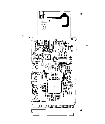
Fig. 1 shows a PCMCIA peripheral card 8 which incorporates a
printed antenna 10 in accordance with the preferred embodiment. The
peripheral card 8 is designed to be inserted into a lap top computer 11, as
shown in Fig. 3.
As shown best in Fig. 2, the peripheral card 8 comprises a printed
circuit board 12 which features two sections, a main section 14 and an
extension section 20.
The main section 14 includes electronic circuitry 16 for driving the
printed antenna 10, i.e. for applying and receiving radio frequency energy to
and from printed antenna 10. The electronic circuitry is mounted on the
main section 14 of the printed circuit board 12 in a known manner, such as
by automated surface mount technology techniques. The main section 14
of the printed circuit board 12 also includes male card edge connector
I:\IPG7\APO\51636\00105\PATEN1'3.DOC
CA 02200675 1997-03-21
-9-
terminals 22 designed to fit into bifurcated female sockets (not shown)
situated in a peripheral card slot of the lap top computer 1 1. As shown in
Fig. 1, the main section 14 of the printed circuit board 12 is also intended
to
be encased in a metal case 23 which fits into the peripheral card slot in the
S laptop computer 11, as shown in Fig.3.
The extension section 20 of the printed circuit board 12 contains the
printed antenna 10. The extension section 20, however, is not intended to
be encased by the metal case 23 or enclosed in or otherwise covered by the
peripheral card slot. Rather, the extension section 20 is covered by a
protective plastic layer (not shown) and is situated such that when the
peripheral card 8 is inserted into the peripheral slot, the extension section
is exposed to the ambient environment in order to allow the printed
antenna 10 to receive or radiate radio frequency energy, as shown in Fig. 3.
Referring additionally to Figs. 4 and 5, the printed antenna 10 is
shown in greater detail. The preferred embodiment of the printed antenna
10 comprises five major components, namely (a) a thin, planar, dielectric
material 25, (b) a microstrip electromagnetic transmission or feedline
structure 28, (c) a main or primary radiating element 30, (d) a secondary
radiating element 32; and (e) a tuning stub 34. These elements are
discussed, in turn, below.
I:~IPG7~AP0~51636\00105~PATENT3.DOC
CA 02200675 1997-03-21
-10-
The thin, planar, dielectric material 25 is provided by the extension
section 20 of the printed circuit board 12. The dielectric material 25, which
includes opposed surfaces 24 and 26, provides a substrate for the printed
antenna 10. In the preferred embodiment, the printed circuit board 12 is
constructed out of "FR4 board", an epoxy-bonded fibreglass, having a
nominal dielectric coefficient e~ of about 4.4. The extension section 20 of
printed circuit board 12 has a nominal board thickness of about 14 mils
(millionths of an inch). However, actual dielectric coefficients and board
thicknesses for printed circuit boards coming off of a high volume
production line can vary by up to 20% or more due to manufacturing
variances. Also, the dielectric constant tends to differ depending upon
frequency, this characteristic being known to those skilled in this art as the
"hook" effect.
The microstrip feedline structure 28 provides a transmission means
for coupling radio frequency energy between the electrical circuitry 16 and
the radiating portion of the printed antenna 10. (For greater certainty, the
term "printed antenna" is intended to include all of the components (a) to (e)
described above, whereas the terms "radiating element" or "radiating portion
of antenna" excludes the feedline structure 28.) The microstrip feed line
structure 28 also provides an impedance matching means for matching the
driving impedance of electrical circuitry 16, which appears to be
I:UPG7~AP0151636\OOIOS~PATENT3.DOC
CA 02200675 1997-03-~1
-11-
approximately 50 ohm to the radiating element, with the impedance of the
radiating element, which is estimated to appear to be about 20 ohm or so to
the electrical circuitry.
S Structurally, the microstrip feedline structure 28 is a two-layered
structure comprising a layer of an electrically conductive material 36, such
as copper, disposed on dielectric surface 24, and a strip (i.e. a relatively
narrow and elongate layer) of electrically conductive material 38, such as
copper, disposed on the opposite dielectric surface 26. The electrically
conductive layer 36 occupies about half of dielectric surface 24 and
provides a ground plane. The electrically conductive strip 38 extends over
the corresponding area defined by the ground plane layer 36, when viewed
along a direction normal to the ground plane. The conductive strip 38, in
conjunction with the ground plane layer 36, thus provides a microstrip
transmission line. In the preferred embodiment, the conductive strip 38 has
three discrete widths, denoted by dimensions 38a, 38b and 38c, along the
length thereof. In this manner, the electrically conductive strip 38, in
conjunction with the ground plane layer 36, provides a "double stubbed"
feedline structure, as is known in the art, for matching the impedances of
the electrical circuitry 16 and the radiating element.
I:\IPG7\APO\51636\00105\PATENT3.DOC
CA 02200675 1997-03-21
-12-
The main radiating element 30 is composed of a second strip (i.e. a
relatively narrow and elongate layer) of electrically conductive material 40,
such as copper, which is disposed on dielectric surface 26 and is electrically
connected to the feedline structure 28. In practice, conductive strip 40 is
continuous with conductive strip 38, but is referred to herein as a "second"
strip in order to define this portion of the printed antenna 10. Conductive
strip 40, however, is disposed such that it does not extend over the ground
plane layer 36, when viewed along a direction normal to the ground plane.
The conductive strip 40 is preferably composed of two sequential,
continuous, generally linear segments 42 and 44 which preferably have the
same length and are angled with respect to one another, preferably at an
angle of 90°. Thus, the main radiating element of the preferred
embodiment of the printed antenna resembles a "V" in shape. The linear
segments 42 and 44 are also preferably angled with respect to a
longitudinal axis 46 of the feedline structure 28 such that a bisector axis 48
of the main radiating element lies transverse to the main feedline
longitudinal axis 46. This geometry minimizes the longitudinal breadth 52 of
the radiating element. In addition, the main radiating element 30 is stepped
or boustrophedonically shaped at its periphery in order to enhance radiation
therefrom as is known per se in the art.
I:\IPG'TAPO\51636\00105\PA1'ENT3.DOC
CA 02200675 1997-03-21
-13-
The secondary radiating element 32 of the printed antenna is
composed of a third strip of electrically conductive material 50, such as
copper, which is electrically connected to the main radiating element 30 and
in practice is continuous with conductive strip 40. Conductive strip 30 can
be any shape, but in the interests of economising surface area, is bent to
return towards the feedline structure 28. Thus, the overall appearance of
the preferred embodiment of the printed antenna structure 10, including the
feedline structure 28, resembles the shape of a hook or question mark ("?")
composed of a sequentially connected series of substantially linear
segments.
The tuning stub 34 is in essence a terminating portion of the third
conductive strip 50. The printed antenna 10 can be adjusted to radiate
within a given frequency band by adjusting the length of tuning stub 34. To
achieve a carrier or center frequency fo having a centre wavelength Ao, it has
been found that the overall length of the radiating portion of the antenna
(i.e., excluding the feedline structure 28) should be made approximately but
not necessarily exactly, X0/2, where ~o is equal to
* ~ , c being the speed of light
Er fo
I:\IPG71AP0\51636\00105\PAT'ENT3.DOC
CA 02200675 1997-03-21
-14-
The fact that the overall length of the radiating portion of the antenna with
a
carrier frequency fo is not exactly equal to X0/2 may be thought or theorized
by some skilled in the art to be due to the effect of fringing fields at the
edges of the radiating antenna, but of course other physical phenomenon
may account for this characteristic. Nevertheless, the precise frequency
range of the antenna can be adjusted by the relatively minute shortening or
lengthening of tuning stub 34. For example, the applicant has been able to
attain a centre frequency of 2.437 GHz with a radiating element
approximately 2.4 cm long using a printed circuit board having a nominal
dielectric co-efficient of 4.4 and a nominal thickness of 14 mils. Such a
frequency is typical of carrier frequencies in emerging wireless data
communication standards.
The advantages and utility of the printed antenna 10 to solve a
number of conflicting design constraints are now discussed in greater detail.
First, unlike microstrip patch antennas, the radiating portion of the
printed antenna 10 is not disposed directly over a ground plane. Thus,
compared to microstrip patch antennas, the tuned or center frequency of
the printed antenna 10 will be relatively intolerant to variations in the
dielectric constant of the printed circuit board.
I:~IPG71AP0151636~OOlOS~PATENT3.DOC
CA 02200675 1997-03-21.
-15-
Second, because the radiating portion of the printed antenna 10 is
not disposed over a ground plane, the printed antenna 10 can radiate in
both upper and lower hemispheres with respect to the plane of the antenna.
Figs. 7A-7F are graphical plots of the electric field components Ee and E~
for an embodiment of printed antenna 10 having a radiating element
approximately 2.5 cm long. (The plots were conducted with respect to an
isolated antenna, i.e. not being inserted into the laptop computer. The
computer, do to its three dimensional characteristics, will have some effect
on the radiating characteristics of the printed antenna 10 at frequencies in
the GHz range.) The reference co-ordinate system for these plots is shown
in Fig. 6, the origin being situated at point "O" in Fig. 3 with the x-axis
lying
along the longitudinal axis 46 of the feedline structure 28. The plots were
generated by a commercially available simulator assuming a dielectric
constant of 4.0 and a dielectric material thickness of 0.36 millimetres. It
will be seen from these plots that the printed antenna 10 has an
omnidirectional radiation pattern exhibiting good radiation dispersion
characteristics.
It may be theorized by some skilled in the art that the radiation
dispersion characteristics of the printed antenna 10 are due mainly to the
shape of the main radiating element 30. As mentioned, the segments 40
and 42 of the main radiating element 30 are angled with respect to one
I:~IPG7~AP0~.51636\OOIOS~PATENT3.DOC
CA 02200675 1997-03-21
- 16-
another, and are preferably orthogonal to one another. Such a geometry
permits the direction of induced currents in the segments 40 and 42 to be
orthogonal to one another and hence enables the main radiating element to
collect or couple energy over a wide region of space, as opposed to a
strictly linear radiating element which cannot collect linearly polarized
electromagnetic energy in which the electric field is orthogonal to the linear
radiating element. Thus, the inclined segments 40 and 42 provide a wide
dispersion radiation pattern for use in a multi-path environment where it is
assumed that the probability of the incident angle of the electric field
component of a received electromagnetic wave is substantially the same
over any region of space. Such channel characteristics are common in
many wireless data communication environments.
Third, because the radiating portion of the printed antenna 10 is not
situated over a ground plane, the antenna 10 does not present a highly
resonant thin cavity structure. Instead, the printed antenna 10 presents a
partially resonant structure as compared to the highly resonant nature of
microstrip patch antennas. Therefore, the printed antenna 10 is relatively
intolerant to variations in the thickness of the printed circuit board 12,
which can be relatively substantial for printed circuit boards manufactured
on high volume production lines. This means that the printed antenna 10
can provide a relatively wide bandwidth even when a very thin printed
I:\IPG7\APO\51636\00105\PATENT3.DOC
CA 02200675 1997-03-21
-17-
circuit board is used as is apt to occur in the latest generation of wireless
data communication products. Fig. 7 shows a plot of the stimulated return
loss of the particular embodiment of printed antenna 10 having a radiating
element length of approximately 2.5 cm and a total length approximately 7
cm long, which, as shown, produces a center frequency of about 2.6 GHz.
((The plot was conducted with respect to an isolated antenna.) It will be
seen that the predicted bandwidth for this particular embodiment, typically
defined as the 3 dB loss from the gain of the antenna at the center or notch
frequency, is about 150 MHz, or 6% of the center frequency.
Fourth, the longitudinal and latitudinal breadths of the radiating
portions of printed antenna 10, respectively denoted by dimensions 52 and
54, are relatively small, each being only roughly X0/6 long, thereby
occupying a relatively small surface area. In contrast, the longitudinal and
latitudinal breadths of the radiating portions of a microstrip patch antenna
are each about Ao/2 long. The relatively small surface area required by
printed antenna 10 is convenient for the design of small, portable, wireless
data communications devices such as the PCMCIA peripheral card 8 for
laptop computer 11.
While the preferred embodiment of the printed antenna has been
described with a certain particularity for the purposes of illustration, it
will
I:~IPG7~AP0~51636~OOlOS~PAT'EN'T3.DOC
CA 02200675 1997-0 ,
-18-
be noted that various modifications may be made thereto while keeping
within the spirit of the invention. For example, while the conductive
material composing the radiating portion of printed antenna 10 has been
shown to be located on dielectric surface 26, the conductive material may
also be disposed on dielectric surface 24 provided there is no contact with
the conductive ground layer 36. Also, while the various conductive
segments comprising the printed antenna 10 have been illustrated as
substantially straight lines, it should be appreciated that the segments may
be somewhat arcuate at their peripheries provided that each segment
remains generally linear from starting point to end point. As a further
example, while the transmission means and impedance matching means
have been shown to be the feedline structure 28, it will be appreciated that
various other structures, such as a co-axial feedline, baluns, and quarter
wave matching structures, can accomplish such functionality and are
intended within the scope of such means. The scope of the invention is
defined by the claims which follow.
I:\IPG71AP0\51636\00105\PATENT'3.DOC