Language selection

Search

Patent 2200866 Summary

Third-party information liability

Some of the information on this Web page has been provided by external sources. The Government of Canada is not responsible for the accuracy, reliability or currency of the information supplied by external sources. Users wishing to rely upon this information should consult directly with the source of the information. Content provided by external sources is not subject to official languages, privacy and accessibility requirements.

Claims and Abstract availability

Any discrepancies in the text and image of the Claims and Abstract are due to differing posting times. Text of the Claims and Abstract are posted:

  • At the time the application is open to public inspection;
  • At the time of issue of the patent (grant).
(12) Patent: (11) CA 2200866
(54) English Title: OPTICAL DATA CONNECTION BETWEEN ADJACENT SUBASSEMBLIES
(54) French Title: LIAISON OPTIQUE DE TRANSMISSION DE DONNEES ENTRE DES SOUS-ENSEMBLES ADIACENTS
Status: Expired and beyond the Period of Reversal
Bibliographic Data
(51) International Patent Classification (IPC):
  • G02B 6/43 (2006.01)
(72) Inventors :
  • SCHRECK, HANS-GUNTHER (Germany)
  • GRUHLER, ULRICH (Germany)
(73) Owners :
  • SIEMENS AKTIENGESELLSCHAFT
(71) Applicants :
  • SIEMENS AKTIENGESELLSCHAFT (Germany)
(74) Agent: SMART & BIGGAR LP
(74) Associate agent:
(45) Issued: 2007-01-09
(86) PCT Filing Date: 1995-09-12
(87) Open to Public Inspection: 1996-04-04
Examination requested: 2002-09-03
Availability of licence: N/A
Dedicated to the Public: N/A
(25) Language of filing: English

Patent Cooperation Treaty (PCT): Yes
(86) PCT Filing Number: PCT/DE1995/001247
(87) International Publication Number: WO 1996010302
(85) National Entry: 1997-03-24

(30) Application Priority Data:
Application No. Country/Territory Date
P 44 34 358.2 (Germany) 1994-09-26

Abstracts

English Abstract


In order to seduce the number of multiple plug-in
connectors in an optical data-link between adjacent
component assemblies, the invention calls for at least
one suitably modulated beam of light (SK) to be radiated
by one assembly (BGL) to the adjacent assembly (BGL)
through the space between the assemblies (BGL).


French Abstract

Afin de réduire le nombre de fiches multibroches complexes de connexion, au moins un faisceau de lumière (SK) modulé de manière appropriée est transmis par un sous-ensemble (BGL) à un sous-ensemble adjacent (BGL) à travers l'espace qui sépare les sous-ensembles adjacents (BGL).

Claims

Note: Claims are shown in the official language in which they were submitted.

-6-
claims
1. Optical data connection between adjacent
subassemblies (BGL) which are arranged parallel and side
by side within a subassembly frame, in which connection
at least one correspondingly modulated light beam is
emitted through the interspace between adjacent
subassemblies (BGL) from one subassembly (BGL) to the
adjacent subassembly (BGL), at least one transmitting
module (SO) having a laser diode arrangement which emits
a slightly divergent light beam being arranged on one
subassembly (BGL), and at least one receiving module (EO)
having a photodiode arrangement being arranged on the
opposite subassembly (BGL), characterized in that, on one
side of each subassembly (BGL) there is provided a
single-part transmitting and receiving module (SEM)
having a laser diode arrangement (LD) and a photodiode
arrangement (PD), the laser diode arrangement (LD) and
the photodiode arrangement (PD) being arranged within the
transmitting and receiving module (SEM), lying parallel
to the subassembly printed circuit board (BGL) and being
arranged opposite each other offset by a specific amount,
surface plane mirrors (SP) for deflecting the light beams
through 90 degrees being provided between these two
arrangements in the respective beam paths, and in that
one of the light beams (SK) passes through an aperture
(D) in the subassembly printed circuit board (BGL).
2. Optical data connection according to Claim 1,
characterized in that the transmitting and receiving
module (SEM) contains a plurality of laser diode arrange-
ments and photodiode arrangements (LD, PD) side by side.

Description

Note: Descriptions are shown in the official language in which they were submitted.


22008~b
94 P 1707
Description
Optical data connection between adjacent subassemblies
The invention relates to an optical data connec-
tion between adjacent subassemblies which are arranged
parallel and side by side within a subassembly frame, in
which connection at least one correspondingly modulated
light beam is emitted through the interspace between
adjacent subassemblies from one subassembly to the
adjacent subassembly, at least one transmitting module
having a laser diode arrangement which emits a slightly
divergent light beam being arranged on one subassembly,
and at least one receiving module having a photodiode
arrangement being arranged on the opposite subassembly.
An optical data connection of this type is known,
for example, from DE 37 39 629 A1. However, in the case
of this known optical data connection, transmission can
take place in only one direction, since each subassembly
has a transmitting module only on one side and a
receiving module on the other side.
However, optical data connections between adjac-
ent subassemblies are already known (see, for example,
"Optoelectronic interconnection based on a light-guiding
plate with holographic coupling elements", Optical
engineering 30 (10), 1620-1623 (October 1991)) which
permit duplex operation. In this case, the optical
connection is carried out via a light-guiding glass plate
in the back plane printed circuit board. In this case
there are considerable problems in the coupling of the
light beams into and out of the light-guiding glass
plate.
It is therefore the object of the present inven-
tion to specify an ogtical data connection between
adjacent subassemblies of the type mentioned at the
beginning which is distinguished by a simple construction
and permits transmitting and receiving operation in both
directions.

2200866
GR 94 P 1707 - 2 -
P44 34 358.2-35
This object is achieved in the case of an optical
data connection of the type mentioned at the beginning by
providing on one side of each subassembly a single-part
transmitting and receiving module having a laser diode
arrangement and a photodiode arrangement (PD), the laser
diode arrangement and the photodiode arrangement being
arranged within the transmitting and receiving module,
lying parallel to the subassembly printed circuit board
and being arranged opposite each other offset by a
specific amount, surface plane mirrors for deflecting the
light beams through 90 degrees being provided between
these two arrangements in the respective beam paths, and
one of the light beams passing through an aperture in the
subassembly printed circuit board.
The optical data connection according to the
invention is distinguished by a simple construction. As
a result of the fact that a single module is needed for
transmitting and receiving and apertures in the
subassembly are provided at the place of mounting of the
module, a single module can transmit and receive in both
directions.
DE 39 08 786 A1 has already disclosed a method of
information transmission between circuit boards of an
electronic circuit. However, the components for carrying
out this known information transmission method cannot be
constructed in modular fashion. Moreover, the known
method is not position-tolerant and exhibits considerable
transmission losses. In addition, it is not easy to
implement in practice.
An advantageous refinement of the optical data
connection according to the invention can be character-
ized in that
AMENDED SHEET

2200866
GR 94 P 1707 - 3 -
P44 34 358.2-35
the transmitting and receiving module contains a
plurality of laser diode arrangements and photodiode
arrangements side by side.
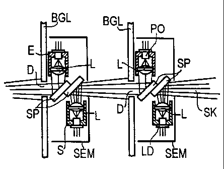
The invention is described in more detail below
using an exemplary embodiment shown in the figure.
In the figures:
FIG 1 shows the basic construction of an optical data
connection according to the present invention,
and
FIG 2 shows the basic construction of transmitting and
receiving modules for the construction of an
optical data connection, the modules being able
to transmit and receive in both directions.
FIG 1 shows the basic construction of an optical
data connection according to the present invention
between two subassembly printed circuit boards BGL, which
are arranged parallel and side by side. Arranged on each
printed circuit board are transmitting locations SO and
receiving locations EO, opposite which corresponding
AMENDED SHEET

2200866
- 4 -
EO and transmitting locations SO lie on the other
subassembly printed circuit board. In FIG 1, the expan-
sion of the beam can be seen, as a result of which the
optical connection is tolerant in terms of position and
does not have to be adjusted. The expansion is optimized
to the maximum received power at given tolerances and
connection lengths.
The transmitting location essentially comprises
a laser diode and the receiving location essentially
comprises a photodiode. A plurality of transmitting
locations SO and receiving locations SO can be accommo-
dated within one transmitting and receiving module SEM.
FIG 2 shows in principle a particularly expedient
construction of such transmitting and receiving modules.
To form the light beam, lenses L are combined both with
the laser diodes LD and with the photodiodes PD. These
lenses are in each case integrated with a laser diode LD
or with a photodiode PD in a submodule. This integration
can also include the electronics necessary for the
electro-optic conversion. In the case of the embodiment
of transmitting and receiving modules SEM shown in FIG 2,
the submodules are arranged lying down, in order to
reduce the module constructional height. The deflection
into the emission directions is carried out via surface
plane mirrors SP. Here, all the necessary components are
arranged in one single module. The module SEM can be
fitted to both sides of a subassembly in order to produce
connections to both sides. If, as is shown in FIG 2,
apertures are provided in the subassembly printed circuit
board and in the corresponding housing wall of the
module, a single module can transmit and receive in both
directions.
In this arrangement, a module can contain a
plurality of transmitting and receiving channels side by
side, the minimum channel separation being able to lie in
the range from 5 to 10 mm.
Finally, the advantages of the optical data
connection according to the invention are summarized once
more:

CA 02200866 2006-05-18
20365-3681
The optical connections to adjacent subassemblies need no
longer be led via the back plane, the back plane is
relieved, the routing on the subassembly is simplified. The
optical connection can transmit almost arbitrarily high data
5 rates, the restriction lying exclusively in the electro-
optic converters.
Transmitting and receiving modules can be arranged
arbitrarily on the subassembly printed circuit board, even
directly in the vicinity of high-frequency sources and
sinks.
Impedance matching problems are dispensed with in the case
of the optical data connection.
The optical data connection is a contactless connection, as
a result of which the use of plug and socket connectors is
dispensed with.
Cross-talk on parallel channels is negligible, even at high
frequencies, and is independent of the data rate.
In accordance with this invention, there is provided an
optical data connection between adjacent subassemblies (BGL)
which are arranged parallel and side by side within a
subassembly frame, in which connection at least one
correspondingly modulated light beam is emitted through the
interspace between adjacent subassemblies (BGL) from one
subassembly (BGL) to the adjacent subassembly (BGL), at
least one transmitting module (SO) having a laser diode
arrangement which emits a slightly divergent light beam
being arranged on one subassembly (BGL), and at least one
receiving module (EO) having a photodiode arrangement being
arranged on the opposite subassembly (BGL), characterized in
that, on one side of each subassembly (BGL) there is
provided a single-part transmitting and receiving module

CA 02200866 2006-05-18
20365-3681
5a
(SEM) having a laser diode arrangement (LD) and a photodiode
arrangement (PD), the laser diode arrangement (LD) and the
photodiode arrangement (PD) being arranged within the
Y
transmitting and receiving module (SEM), lying parallel to
the subassembly printed circuit board (BGL) and being
arranged opposite each other offset by a specific amount,
surface plane mirrors (SP) for deflecting the light beams
through 90 degrees being provided between these two
arrangements in the respective beam paths, and in that one
of the light beams (SK) passes through an aperture (D) in
the subassembly printed circuit board (BGL).

Representative Drawing
A single figure which represents the drawing illustrating the invention.
Administrative Status

2024-08-01:As part of the Next Generation Patents (NGP) transition, the Canadian Patents Database (CPD) now contains a more detailed Event History, which replicates the Event Log of our new back-office solution.

Please note that "Inactive:" events refers to events no longer in use in our new back-office solution.

For a clearer understanding of the status of the application/patent presented on this page, the site Disclaimer , as well as the definitions for Patent , Event History , Maintenance Fee  and Payment History  should be consulted.

Event History

Description Date
Inactive: IPC expired 2013-01-01
Time Limit for Reversal Expired 2012-09-12
Letter Sent 2011-09-12
Appointment of Agent Requirements Determined Compliant 2010-05-20
Revocation of Agent Requirements Determined Compliant 2010-05-20
Inactive: Office letter 2010-05-18
Revocation of Agent Request 2010-03-09
Appointment of Agent Request 2010-03-09
Grant by Issuance 2007-01-09
Inactive: Cover page published 2007-01-08
Inactive: Final fee received 2006-10-11
Pre-grant 2006-10-11
Amendment After Allowance Requirements Determined Compliant 2006-06-21
Letter Sent 2006-06-21
Inactive: Amendment after Allowance Fee Processed 2006-05-18
Amendment After Allowance (AAA) Received 2006-05-18
Letter Sent 2006-04-18
Notice of Allowance is Issued 2006-04-18
Inactive: IPC from MCD 2006-03-12
Inactive: Approved for allowance (AFA) 2006-01-23
Letter Sent 2002-10-15
Request for Examination Received 2002-09-03
Request for Examination Requirements Determined Compliant 2002-09-03
All Requirements for Examination Determined Compliant 2002-09-03
Letter Sent 1997-09-11
Inactive: Notice - National entry - No RFE 1997-06-19
Inactive: First IPC assigned 1997-06-18
Inactive: IPC assigned 1997-06-18
Inactive: Applicant deleted 1997-06-10
Inactive: Notice - National entry - No RFE 1997-06-10
Inactive: Single transfer 1997-05-06
Inactive: Courtesy letter - Evidence 1997-04-22
Application Published (Open to Public Inspection) 1996-04-04

Abandonment History

There is no abandonment history.

Maintenance Fee

The last payment was received on 2006-08-14

Note : If the full payment has not been received on or before the date indicated, a further fee may be required which may be one of the following

  • the reinstatement fee;
  • the late payment fee; or
  • additional fee to reverse deemed expiry.

Please refer to the CIPO Patent Fees web page to see all current fee amounts.

Owners on Record

Note: Records showing the ownership history in alphabetical order.

Current Owners on Record
SIEMENS AKTIENGESELLSCHAFT
Past Owners on Record
HANS-GUNTHER SCHRECK
ULRICH GRUHLER
Past Owners that do not appear in the "Owners on Record" listing will appear in other documentation within the application.
Documents

To view selected files, please enter reCAPTCHA code :


To view images, click a link in the Document Description column. To download the documents, select one or more checkboxes in the first column and then click the "Download Selected in PDF format (Zip Archive)" or the "Download Selected as Single PDF" button.

List of published and non-published patent-specific documents on the CPD .

If you have any difficulty accessing content, you can call the Client Service Centre at 1-866-997-1936 or send them an e-mail at CIPO Client Service Centre.


Document
Description 
Date
(yyyy-mm-dd) 
Number of pages   Size of Image (KB) 
Representative drawing 1997-10-30 1 5
Abstract 1997-03-24 1 7
Claims 1997-03-24 1 44
Description 1997-03-24 5 179
Drawings 1997-03-24 1 18
Cover Page 1997-10-30 1 32
Drawings 1997-03-25 1 17
Description 2006-05-18 6 217
Representative drawing 2006-12-05 1 11
Cover Page 2006-12-05 1 37
Notice of National Entry 1997-06-19 1 202
Notice of National Entry 1997-06-10 1 202
Courtesy - Certificate of registration (related document(s)) 1997-09-11 1 118
Reminder - Request for Examination 2002-05-14 1 118
Acknowledgement of Request for Examination 2002-10-15 1 176
Commissioner's Notice - Application Found Allowable 2006-04-18 1 162
Maintenance Fee Notice 2011-10-24 1 171
PCT 1997-03-24 8 223
Correspondence 1997-04-22 1 36
PCT 1997-08-14 6 148
PCT 1997-03-24 17 523
Fees 1997-09-11 1 33
Correspondence 2006-10-11 1 40
Correspondence 2010-03-09 11 652
Correspondence 2010-05-18 6 411
Correspondence 2010-05-18 1 29