Note: Descriptions are shown in the official language in which they were submitted.
~200~~!
-1-
CIRCUIT ARRANGEMENT FOR OPERATING ELECTRIC LAMPS, AND
AN OPERATING METHOD FOR ELECTRIC LAMPS
FIELD OF THE INVENTION
The invention relates to a circuit arrangement for
operating electric lamps, and to an operating method
for electric lamps.
BACKGROUND OF THE INVENTION
Such a circuit arrangement is disclosed, for example,
in European Patent EP 0 113 451. An inverter having a
load circuit containing a discharge lamp and having a
series resonant circuit connected to the inverter
output is described in this publication. In order to
limit the no-load voltage in this series resonant
circuit, use is made of a series circuit which
comprises a varistor and a capacitor and is arranged in
a parallel branch relative to the resonance capacitor.
The series circuit comprising the varistor and the
capacitor varies the resonance capacitance active in
the resonant circuit and thus ensures that the resonant
220903
_2_
frequency of the series resonant circuit is shifted
independently of voltage. However, this series
arrangement requires a voluminous and comparatively
expensive varistor for each series resonant circuit.
SU1~IARY OF THE INVENTION
It is the object of the invention to provide a circuit
arrangement for operating electric hamps which ensures
in as simple and cost-effective a way as possible in
the load circuit connected to the inverter output an
effectively controllable no-load voltage with low
tolerances and, in particular, a limiting both of the
no-load voltage and of the voltage with respect to the
neutral conductor which satisfies the general safety
requirements.
The operating method according to the invention for
electric lamps in a circuit arrangement which has a
self-oscillating inverter with current feedback, having
at least two alternately switching transistors and a
load circuit connected to the inverter output and
designed as a resonant circuit, is distinguished in
that a limiting of the no-load voltage in the load
circuit is achieved by varying the emitter resistance
200903
-3-
or source resistance of one of the inverter transistors
as a function of the voltage drop across one of the
resonant circuit components, the clock frequency of the
inverter thereby also being varied, with the result
that the difference between the inverter clock
frequency and the resonant frequency of the resonant
circuit is increased.
In order to realize this operating method, according to
the invention the circuit arrangement has a transistor
- advantageously a field-effect transistor - whose
control junction is arranged in the emitter line of one
of the inverter transistors. The control input of this
transistor is connected via a first current path to a
voltage source and is connected, via a second current
path, to a voltage divider which is connected to a
resonant circuit component via a tap in the load
circuit. Via the conductivity of the control junction
of this transistor, that is to say the drain-source
junction or the collector-emitter path, during normal
operation of the circuit arrangement the emitter
resistance of the corresponding inverter transistor,
and thus the clock frequency of the self-oscillating
inverter, is adjusted using current feedback. If, in
the load circuit designed as a resonant circuit, the
~~~~9~~
-4-
no-load voltage overshoots a value prescribed by the
dimensioning of the circuit components, the input
signal for the control electrode, that is to say the
gate electrode or base electrode, of the transistor
arranged in the emitter line of the inverter transistor
is varied with the aid of the trigger. As a result,
there is a variation in the conductivity of the drain-
source junction or the collector-emitter path of this
transistor, and also the emitter resistance of the
corresponding inverter transistor, as well as the clock
frequency of the self-oscillating inverter with current
feedback. The change in the inverter clock frequency
takes place in this case such that the difference
between the inverter clock frequency and resonant
frequency of the load circuit designed as a resonant
circuit increases. This frequency detuning is attended
by a reduced no-load voltage in the load circuit. The
no-load voltage in the load circuit can advantageously
be adjusted to the desired value by a suitable
selection of voltage divider resistors which are
arranged in the abovementioned first and/or second
current path ending at the control input of the
transistor according to the invention. The general
safety requirements in accordance with the regulation
EN 60 928 can be fulfilled thereby.
2200903
-5-
Thus, the clock frequency of the inverter is adjusted
via the electric conductivity of the drain-source
junction or the collector-emitter path of the
transistor according to the invention arranged in the
emitter line or source line of one of the inverter
transistors in such a way that the no-load voltage in
the load circuit does not overshoot the value
prescribed by the dimensioning of the corresponding
electronic components. A first - the negative - half-
wave of the resonance capacitor voltage is
advantageously employed to regulate or limit the no-
load voltage.
The transistor arranged according to the invention in
the emitter line or source line of one of the inverter
transistors does not, however, serve only to limit the
no-load voltage in the load circuit designed as a
resonant circuit, but advantageously additionally also
undertakes to switch off the inverter upon the
occurrence of an anomalous operating state of the
circuit arrangement. For this purpose, the circuit
arrangement according to the invention has a bistable
switching device whose output is connected via a third
current path to the control input of the transistor
2200903
-6-
arranged in the emitter line or source line of one of
the inverter transistors, while there is present at the
input of this bistable switching device an electric
voltage which is proportional to the time-averaged
second - the positive - half-wave of the resonance
capacitor voltage of the load circuit.
Thus, the transistor according to the invention
arranged in the emitter line or source line of one of
the inverter transistors undertakes two different
functions.
During normal operation of the circuit arrangement, it
operates as an element controlled in analog fashion by
virtue of the fact that it assumes different low-
resistance states depending on the no-load voltage in
the load circuit and thereby varies the inverter clock
frequency, while given the occurrence of a fault it
operates as a switch and goes over into the high-
resistance state in order to interrupt the oscillation
of the inverter.
HRIEF DESCRIPTION OF THE DRAWINGS
2~~~9(~3
The invention is explained below in more detail with
the aid of a preferred exemplary embodiment. In the
drawing:
Figure 1 shows a diagrammatic sketched circuit diagram
of the principle of the invention, and
Figure 2 shows a preferred exemplary embodiment of the
circuit arrangement according to the
invention.
BEST MODE FOR CARRYING OUT THE INVENTION
The principle of the circuit arrangement according to
the invention is explained below in more detail with
the aid of Figure 1, which shows a diagrammatic
sketched circuit diagram for the operation of a low-
pressure discharge lamp. This circuit arrangement has
a half-bridge inverter fitted with two bipolar
transistors Q1, Q2. The two bipolar transistors Q1, Q2
are respectively equipped with a freewheeling diode D1,
D2 which are connected in parallel with the collector-
emitter path of the corresponding transistor Q1, Q2.
In addition, the two bipolar transistors Q1, Q2
respectively have an emitter resistor R3, R4 and a
~2Q~9~~
_8_
base-emitter parallel resistor R5, R6. An ohmic
resistor R7 and a capacitor C2 are, furthermore,
connected in parallel with the collector-emitter path
of the transistor Q1.
The two switching transistors Q1, Q2 of the half bridge
are driven by means of a toroidal-core transformer
which has one primary winding RKa and two secondary
windings RKb, RKc. The primary winding RKa is
integrated into the series resonant circuit of the
half-bridge inverter, which is connected to the centre
tap M of the inverter and contains the coupling
capacitor CK, the resonance inductor L1 and the
resonance capacitor C1. The secondary windings RKb,
RKc are respectively integrated into the base-emitter
circuit of an inverter transistor Q1, Q2 and connected
in each case via a base series resistor R1, R2 and an
inductor L2, L3 to the base terminal of the relevant
bipolar transistor Q1, Q2. The half-bridge inverter
further has a .starting device which essentially
comprises the diac DC and the starting capacitor C3.
The diac DC is connected via the conductor L3 to the
base terminal of the inverter transistor Q2. One
terminal of the starting capacitor C3 is connected to
the negative pole of the inverter DC voltage supply,
z2oo9o~
_g_
while its other terminal is connected, on the one hand,
via an ohmic resistor R10 and a rectifier diode D3 to
the centre tap M of the half bridge and, on the other
hand, via an ohmic resistor R8 and the electrode coil
E2 of the low-pressure discharge lamp LP to the
positive pole of the inverter DC voltage supply.
The fluorescent lamp LP to be operated is connected in
parallel with the resonance capacitor C1. One terminal
of the first electrode coil E1 of the lamp LP is
connected to the resonance inductor L1, while the other
terminal of the first electrode coil E1 is connected to
the resonance capacitor C1. One terminal of the second
lamp electrode coil E2 is connected to the positive
pole of the inverter DC voltage supply, and the other
terminal of the second lamp electrode coil is connected
via an ohmic resistor R8 to the starting capacitor C3.
To this extent, the circuit arrangement corresponds to
a half-bridge inverter as described, for example, on
pages 62-63 of the book entitled "Schaltnetzteile"
["Switched-mode power supplies"] by W. Hirschmann/A.
Hauenstein, publisher Siemens AG.
2~4~90
After switching on, the starting capacitor C3 is
charged to the breakdown voltage of the diac DC, which
then generates trigger pulses for the base of the
bipolar transistor Q2 and thereby causes the half-
bridge inverter to oscillate. After the transistor Q2
has switched through, the starting capacitor C3 is
discharged via the resistor R10 and the diode D3 so far
that the diac D3 no longer generates trigger pulses.
The two inverter transistors Q1, Q2 switch alternately,
with the result that the centre tap M of the half
bridge is alternately connected to the positive pole or
negative pole of the DC voltage supply. The recharging
of the coupling capacitor CK brought about thereby
causes in the series resonant circuit and in the lamp
LP a mid-frequency alternating current whose frequency
corresponds to the clock frequency of the half-bridge
inverter. The clock frequency of the half-bridge
inverter is normally more than 20 kHz. The electronic
components of the circuit arrangement according to the
invention are, furthermore, dimensioned such that the
clock frequency of the self-oscillating half-bridge
inverter is above the resonant frequency of the series
resonant circuit L1, C1.
220090
-11-
Connected into the emitter line of the second half-
bridge transistor Q2 is a field-effect transistor T1
with the aid of which the effective emitter resistance
of the second half-bridge transistor Q2 can be varied.
The drain terminal of this field-effect transistor T1
is connected via the emitter resistor R4 to the emitter
of the switching transistor Q2. The source terminal of
the field-effect transistor T1 is earthed or connected
to the negative pole of the DC voltage supply of the
inverter. The gate of the field-effect transistor T1
is connected to the negative pole of the DC voltage
supply via, on the one hand, a zener diode DS serving
as overvoltage protection and, on the other hand, via
an ohmic resistor R14, a zener diode DZ, a branching
point V1 and an ohmic resistor R9. The branching point
V1 is connected to a tap V3 in the series resonant
circuit via a rectifier diode D4 polarized opposite to
the zener diode DZ, a further branching point V2, an
ohmic resistor R12 and a capacitor C4. The tap V3 is
situated between the resonance inductor L1 and the
resonance capacitor C1. The discharge path of the low-
pressure discharge lamp LP is arranged in parallel with
the resonance capacitor C1. The branching point V2 is
connected to the negative pole of the DC voltage supply
via an ohmic resistor R13. The ohmic resistors R9, R12
220090
-12-
and R13 form a voltage divider which is arranged in
parallel with the resonance capacitor and the lamp LP
in terms of alternating current via the capacitor C4.
When the circuit arrangement is switched on, before the
inverter is started, the field-effect transistor T1 is
controlled to be of low resistance via the electrode
coil E2 and the resistors R8 and R11, which connect the
gate of the field-effect transistor T1 to the positive
pole of the DC voltage source. The diac DC transmits
trigger pulses to the base of the second half-bridge
transistor Q2 and thus, as already described above,
causes the half-bridge inverter to oscillate. In the
normal case, the low-pressure discharge lamp will then
ignite after a short time. At the tap V3 in the series
resonant circuit, the voltage drop across the resonance
capacitor C1 or across the lamp LP is detected by the
voltage divider R9, R12, R13 and divided down in
accordance with the resistance values of these ohmic
resistors. As long as the amplitude of the resonance
capacitor voltage undershoots a critical value, which
can be adjusted to a desired value by a suitable
dimensioning of the resistors R9, R13 and R14, the
zener diode DZ, and thus also the current path which
leads, starting from the gate of the field-effect
200903
-13-
transistor T1, via the resistor R14, the zener diode DZ
and the ohmic resistor R9 to the negative pole of the
DC voltage source, remain de-energized, and the field-
effect transistor T1 receives its full control signal
via the resistors RS and R11. If the amplitude of the
resonance capacitor voltage reaches this critical
value, upon traversal of the negative half-wave of the
resonance capacitor voltage the voltage drop between
the gate of the field-effect transistor T1 and the
branching point V2 rises so far that the zener diode DZ
becomes conductive. As a consequence of this, the gate
of the field-effect transistor T1 receives only a
reduced control signal via the resistors R8 and R11,
since a portion of this control signal flows off to the
negative pole of the DC voltage source via the resistor
R14, the zener diode DZ, which is now conductive, and
the voltage divider resistors R9 and R13, which are now
connected in parallel. The rectifier diode D4 is
polarized such that the zener diode DZ reacts
sensitively only. to the negative half-wave of the
resonance capacitor voltage. The strength of the
remaining control signal can, given otherwise unchanged
parameters, be adjusted through the dimensioning of the
resistors R9 and R14. A reduced control signal for the
gate of the field-effect transistor T1 reduces the
200903
-14-
conductivity of the drain-source junction of the field-
effect transistor T1 and thus increases the effective
emitter resistance of the bipolar transistor Q2, since
the effective emitter resistance is essentially an
additive combination of the resistance value of the
ohmic resistor R4 and the resistance value of the
drain-source junction of the field-effect transistor
T1. The consequence of an increased emitter resistance
is that the toroidal-core transformer RK reaches its
magnetic saturation flux density more quickly, and that
thereby the on duration of the half-bridge inverter
transistor Q2 is correspondingly shortened. Thus, an
increase in the effective emitter resistance leads to a
corresponding higher clock frequency of the half-bridge
inverter. Since the clock frequency of the half-bridge
inverter is higher than the resonant frequency of the
series resonant circuit, an increase in the inverter
clock frequency leads to an increase in the frequency
detuning between the resonant frequency of the series
resonant circuit L1, C1 and the clock frequency of the
half-bridge inverter Q1, Q2. The no-load voltage in
the series resonant circuit connected to the inverter
output M is thereby reduced.
220090
-15-
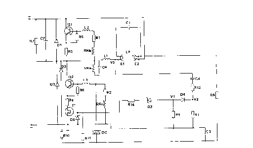
The complete circuit diagram of a circuit arrangement
according to the invention for operating two low-
pressure discharge lamps is represented in Figure 2. A
suitable dimensioning of the electronic components
illustrated here is given in the table. This circuit
arrangement has a self-oscillating half-bridge inverter
with current feedback, which is essentially formed by
two bipolar transistors Q5, Q6, the toroidal-core
transformer RKa, RKb, RKc, the base series resistors
R30, R31 and the emitter resistors R32, R33, and is fed
with a DC voltage. This DC voltage is obtained here
from the mains voltage in a known way by rectification
and subsequent smoothing. The bipolar transistors Q5,
Q6 are equipped in each case with a freewheeling diode
D30, D31 which is connected in parallel with the
collector-emitter path of the corresponding half-bridge
transistor Q5, Q6. Furthermore, the two bipolar
transistors each have a base-emitter parallel resistor
R34, R35 and an inductor L30, L31, which is connected
in series with the base series resistor R30, R31 and is
connected to the base terminal of the corresponding
half-bridge transistor Q5, Q6. A series resonant
circuit which contains the primary winding RKa of the
toroidal-core transformer, the resonance inductor L32
and the resonance capacitor C30 is connected to the
220090
-16-
output of the half-bridge inverter, that is to say
between the centre tap M1 of the half-bridge inverter
transistors Q5, Q6 and the centre tap M2 of the two
coupling capacitors C32, C33.
Two low-pressure discharge lamps LP1, LP2 connected in
series relative to one another are arranged in parallel
with the resonance capacitor C30. the electrode coils
E11, E12 and E21, E22 of these two lamps are preheated
before starting the lamps with the aid of a heating
device H and a heater transformer TR. For this
purpose, the electrode coil E11 of the first low-
pressure discharge lamp LP1 and the electrode coil E22
of the second low-pressure discharge lamp LP2 are
arranged, together with the primary winding of the
heater transformer TR, the bridge rectifier GL and the
heating device H, in a first common heating circuit,
while the other electrode coil E12 of the first low-
pressure discharge lamp LP1 and the other electrode
coil E21 of the second low-pressure discharge lamp LP2
form a second heating circuit together with the
secondary winding of the heater transformer TR. The
electrode coils E11 and E22 respectively have a
capacitor C35, C36 connected in parallel. A starting
capacitor C37 is connected in parallel with the low-
2200903
pressure discharge lamp LP1. The heating device H is
described in detail in Offenlegungsschrift
EP 0 693 864.
The self-oscillating half-bridge inverter is driven
with the aid of the toroidal-core transformer, whose
secondary windings RKb, RKc are respectively arranged
in the base line of one of the half-bridge inverter
transistors Q5, Q6. Starting the half-bridge inverter
is rendered possible by a starting circuit which is
connected to the base terminal of the second half-
bridge inverter transistor Q6 and essentially comprises
the diac DC1, the starting capacitor C34, the ohmic
resistor R36 and the diode D37. One terminal of the
starting capacitor C34 is connected to the negative
pole, which is at system earth of the half-bridge
inverter DC voltage supply, while its other terminal is
connected to the positive pole of the DC voltage supply
via the ohmic resistor R37, the primary winding of the
heater transformer TR, the electrode coil E22 of the
low-pressure discharge lamp LP2 and the ohmic resistor
R3 8 .
The drain-source junction of a field-effect transistor
T2 is arranged in the emitter line of the half-bridge
-18-
inverter transistor Q6, in series with the emitter
resistor R33. The gate of this field-effect transistor
T2 is connected to the positive pole of the DC voltage
supply of the half-bridge inverter via the resistors
R39 and R37, the primary winding of the heater
transformer TR, the electrode coil E22 of the low-
pressure discharge lamp LP2 and the ohmic resistor R38.
The circuit arrangement further has a branch which is
connected in terms of alternating current in parallel
with the resonance capacitor C30 and with the low-
pressure discharge lamps LP1, LP2 and which is
connected to the tap V4 in the resonant circuits and
connected to system earth or to the negative pole of
the DC voltage supply via the resistor R40, the
capacitor C38, the branching point V5, the diode D32,
which is polarized in the forward direction, and the
capacitor C39. The branching point V5 is, moreover,
connected to the negative pole of the DC voltage supply
via the resistor.R4l, and to the gate of the field-
effect transistor T2 via the diode D33, which is
polarized in the reverse direction, the zener diode DZ1
and the resistor R42. The ohmic resistors R40, R41 and
the resistor R51, which is connected in parallel with
the resistor R41 via the diode D33, form a voltage
2200903
-19-
divider which detects the voltage drop across the
resonance capacitor C30. Connected to the centre tap
M1 of the half-bridge inverter is a capacitor C40 which
is connected to a terminal of the capacitor C39 via the
branching point V6 and via the resistor R43. The
branching point V6 is connected via the resistor R44,
the diode D34, which is polarized in the forward
direction, and the zener diode DZ2 to the input of a
bistable switching unit. The bistable switching unit
comprises two bipolar transistors Q7, Q8, the resistors
R45, R46, R47, R48 and the capacitors C41, C42. These
aforesaid components form a thyristor equivalent
circuit whose design and mode of operation are
described, for example, in the book entitled
"Bauelemente der Elektronik and ihre Grundschaltungen"
["Electronic components and their basic circuits"],
pages 395-396, by H. Hoger, S. Kahler, G. Weigt from
the series "Einfiihrung in die Elektronik", Volume 1,
Verlag H. Stam GmbH, 7th edition. The output of this
bistable switching unit is connected to the gate of the
field-effect transistor T2 via the diode D35, which is
polarized in the reverse direction. The two high-
resistance resistors R49 and R50 render it possible for
the capacitors C39 and C34 to be discharged after the
half-bridge inverter has been switched off. A zener
-20-
diode D36 which limits the voltage drop to
approximately 12 V is connected in parallel with the
gate-source junction of the field-effect transistor T2.
The mode of operation of the circuit arrangement illus-
trated in Figure 2 is described below.
Directly after the circuit arrangement is switched on,
the drain-source junction of the field-effect
transistor T2 is controlled to be of low resistance via
the resistor R38, the electrode coil E32, the primary
winding of the heater transformer TR and the resistors
R37 and R39. At the same time, the starting capacitor
C34 is charged to the breakdown voltage of the diac DC1
via the resistor R38, the electrode coil E22, the
primary winding of the heater transformer TR and the
resistor R37, with the result that the diac DC1
generates trigger pulses for the base of the bipolar
transistor Q6 and thereby causes the half-bridge
inverter to oscillate. After the half-bridge inverter
transistor Q6 has been switched through, the starting
capacitor C34 is discharged via the resistor R36 and
the diode D37 so far that the diac DC1 does not
generate any further trigger pulses. The two inverter
transistors Q5, Q6 switch alternately, with the result
2200903
-21-
that their centre tap M1 is alternately connected to
the positive pole and negative pole of the DC voltage
supply of the high-bridge inverter. The result of this
is to generate in the series resonant circuit L32, C30,
which is arranged between the centre tap M1 of the
half-bridge inverter and the centre tap M2 of the
coupling capacitors C32, C33, a mid-frequency
alternating current whose frequency corresponds to the
switching frequency of the half-bridge inverter. The
heating device H and the heater transformer TR ensure
that the electrode coils E11, E12, E21, E22 are
sufficiently preheated with the aid of a heating
current before the ignition of the low-pressure
discharge lamps LP1, LP2. The mode of operation of the
heating device is explained in detail in European
Offenlegungsschrift EP 0 693 864.
According to the invention, the field-effect transistor
T2 fulfils two different functions. Firstly, it is
used to limit or regulate the no-load voltage in the
series resonant circuit, and secondly it is utilized to
switch off the half-bridge inverter as a safety measure
upon the occurrence of an anomalous operating state,
for example in the case of a defective lamp.
~~Oa9~3
-22-
For the purpose of limiting or regulating the no-load
voltage in the series resonant circuit, the voltage
drop across the resonance capacitor C30 is monitored at
the tap V4 with the aid of the components R40, C38,
R41, R51, D33, DZ1, R42. As long as the voltage drop
across the resonance capacitor C30 undershoots the
critical value, the zener diode DZ1 remains blocked and
the field-effect transistor T2 receives its full
control signal. However, if the amplitude of the AC
voltage across the resonance capacitor C30 reaches this
critical value, then while the AC voltage across the
resonance capacitor C30 is traversing the negative
half-wave the voltage drop between the branching point
V5 and the gate of the field-effect transistor T2 will
suffice to permit the zener diode DZ1 to become
conductive. As a result, the control signal for the
gate of the field-effect transistor T2, which is
injected from the positive pole of the DC voltage
supply via the resistor R38, the electrode coil E22,
the primary winding of the heater transformer TR and
the resistors R37, R39, is led off partly via the
resistor R42, the now conducting zener diode DZ1 and
the resistors R41, R51, which are now connected in
parallel through the diode D33, to the negative pole of
the DC voltage supply, and the input signal for the
2200903
-23-
field-effect transistor T2 is corresponding reduced.
The reduced control signal at the gate of the field-
effect transistor T2 reduces the conductivity of the
drain-source junction of the field-effect transistor
T2, and thus increases the effective emitter resistance
of the bipolar transistor Q6 and thereby shortens the
on duration of the transistor Q6, with the result that
the clock frequency of the half-bridge inverter is
increased. Since the clock frequency or switching
frequency of the half-bridge inverter is higher than
the resonant frequency of the series resonant circuit,
the increase in the clock frequency intensifies the
frequency detuning between the clock frequency or
switching frequency of the half-bridge inverter and the
resonant frequency of the series resonant circuit, with
the result that the maximum no-load voltage achievable
by means of the method of resonance amplification is
reduced in accordance with this frequency detuning. It
is possible by means of a suitable dimensioning of the
resistors R42 and.R51 for the strength of the remaining
input signal at the gate of the field-effect transistor
T2, and thus also for the no-load voltage in the series
resonant circuit, to be adjusted to a desired value.
Because of the polarity of the diode D33, only the
negative half-wave of the resonance capacitor voltage
2200903
-24-
is utilized for voltage regulation or voltage
limitation.
In the exemplary embodiment in accordance with Figure 2
and having the dimensioning of the components as speci-
fied in the table, the drain-source junction of the
field-effect transistor T2 has a resistance of
approximately 0.1 W in the fully conducting state, that
is to say that an input voltage of approximately 12 V -
which is the threshold voltage of the zener diode D36 -
is present at the gate. The voltage regulation starts
when the voltage drop across the resonance capacitor
C30 has reached approximately 500 V. If the voltage
drop across the resonance capacitor C30 has risen to
approximately 1000 V, the input signal at the gate of
the field-effect transistor T2 is now only
approximately 4 to 5 V, and the resistance of the
drain-source junction has risen to about 1 W.
In order to switch off the half-bridge inverter Q5, Q6
for safety purposes, use is made, by contrast, of the
positive half-wave of the AC voltage occurring at the
resonance capacitor C30. Switching off for safety pur-
poses in this way is performed synchronously with the
blocking phase of the bipolar transistor Q6 with the
22Q0~~3
-25-
aid of the bistable switching unit Q7, Q8, whose output
is connected to the gate of the field-effect transistor
T2. Present at the input of the bistable switching
unit via the resistor R44, the rectifier diode D34 and
the zener diode DZ2 is the switching-off signal, which
is composed additively from two voltage components.
The first voltage component of the switching-off signal
is a smoothed DC voltage which is proportional to the
voltage drop across the resonance capacitor C30. It is
generated by means of the voltage divider resistors
R40, R41, the capacitor C38 and the diode D32 at the
capacitor C39. The second voltage component of the
switching-off signal is a synchronisation signal which
is proportional to the time-variation in the inverter
output voltage at the centre tap M1. It is generated
with the aid of the components C40 and R43 acting as a
CR differentiating element. The CR series circuit C40,
R43 differentiates the trapezoidal output voltage of
the half-bridge inverter present at the centre tap, and
thereby generates at the resistor R43 a square-wave
voltage which forms the second voltage component of the
switching-off signal. The positive half-wave of this
square-wave voltage is generated by the rising edge,
and the negative half-wave of the square-wave voltage
is generated by the falling edge of the trapezoidal
2zooso3
-2 6-
inverter output voltage. The rising edge of the
trapezoidal inverter output voltage is produced at the
start of the blocking phase of the bipolar transistor
Q6, while the falling edge of the trapezoidal inverter
output voltage is produced at the start of the blocking
phase of the bipolar transistor Q5. The total
switching-off signal is present at the centre tap V6 of
the differentiating element C40, R43, and is fed to the
input of the bistable thyristor equivalent circuit Q7,
Q8 via the components R44, D34 and DZ2. These
components are dimensioned such that in normal
operation the critical threshold voltage of the zener
diode DZ2 is undershot and the bistable switching unit
Q7, Q8 remains deactivated. An anomalous operating
state which has been caused, for example, by a
defective lamp, causes an increased voltage drop across
the capacitor C39. The positive voltage peaks of the
switching-off signal, which are formed by the positive
half-waves, which are added onto the capacitor voltage
at C39, of the square-wave voltage of the
differentiating element C40, R43, then overshoot the
threshold voltage of the zener diode DZ2 and activate
the thyristor equivalent circuit Q7, QB, by means of
which the field-effect transistor T2 and thus also the
half-bridge transistor Q6 are switched off. The half-
~2~U9~3
-27-
bridge inverter is thereby shut down and can only be
restarted by renewed switching-on or by replacing the
defective lamp.
Table: Dimensioning of the electronic components in
accordance with the second exemplary
embodiment, as illust rated in Figure 2
R30, R31 7.5 W
R32 0.47 W
R33 0.39 W
R34, R35, R43 47 W
R36 22 kW
R37, R38 560 kW
R39 330 kW
R40 974 kW
R41 110 kW
R42 120 kW
R44 2.2 kW
R45, R46, R47, R48 10 kW
R49 4.7 kW
R50 1 MW
R51 150 kW
C30 7.5 nF
C32, C33 200 nF
2~0090~
-28-
C34 100 nF
C35, C36 33 nF
C37 330 pF
C38 100 pF
C39 1 mF
C40 33 pF
C41, C42 560 pF
L30, L31 4.7 mH
L32 1.29 mH
RKa, RKb, RKc Toroidal core R 8/4/3.8
D30, D31, D37 1N4946
D32, D33 1N4148
D34, D35 LL4148
D36 Zener diode, 12 V
DZ1, DZ2 Zener diode, 27 V
DC1 1N413M
Q5, Q6 BUF 644
Q7 BC857A
Q8 BC847A
T2 STK14N05