Note: Descriptions are shown in the official language in which they were submitted.
CA 02201048 2001-06-07
Doc. No 18-5 Patent
Broadband Nonhomogeneous Multi-Segmented Dielectric
Resonator Antenna System
Field of the Invention
S
This invention relates generally to dielectric resonator antennas and more
particularly to
an antenna having a high dielectric; material disposed between an antenna feed
and a
dielectric resonator.
Background of the Invention
The rapid growth of information technology has been the main thrust for many
advances
in communication system developments such as satellite, wireless/mobile, and
personal
communications. Systems have been envisioned which will allow the
communication
from any time and place. In many of these systems the final point of contact
is usually a
wireless loop where antennas will play a crucial role. This puts a high demand
on the
antenna performance.
Ensuring efficient system operation requires an increased level of antenna
integration into
the system design right from the inception stage. The demand for high
efficiency,
compact size, low profile, and conformal construction is increasing. It is
also very
desirable for the antenna to be amenable to various arrangements of device
integration as
well as being capable of accommodating various operational requirements.
Presently,
these requirements are likely achieved by arrays of antenna candidates, which
currently
are mostly limited to printed structures. The most popular candidate is a
microstrip
antenna due to fabrication simplicity, low profile, and ease of integration
with many
devices. It is widely used for applications requiring frequencies ranging from
L-Band to
millimeter-waves. However, conventional microstrip antennas are known to
suffer from a
number of disadvantages such as narrow bandwidth, low efficiencies, and higher
loss at
millimeter-wave frequencies. Recently, a relatively new approach to building
microwave
antennas based on the use of a dielectric resonator (DR) as the radiating
element has been
1
CA 02201048 2001-06-07
Doc. No 18-5 Patent
proposed by S.A. Long, M. McAllister, and L.C. Shen, in a paper entitled 'The
resonant
cylindrical dielectric cavity antenna', IEEE Trans. Antennas Prvpagat., Vol.
AP-31, pp.
406-412,1983. Dielectric resonators (DRs) have been in use for a long time in
microwave
circuits mainly as energy storage devices. However, since DR boundaries are
not
conductors, there exists a 'loss' mechanism which forms the basis of their use
as radiating
elements. DRs have been found to overcome some disadvantages of microstrip
antennas.
They also posses:> the attractive features of microstrip patches but offer
superior
performance, particularly, in terms of bandwidth and radiation efficiency.
Dielectric Resonator Antennas (DRAs) are antennas fabricated entirely from low
loss
dielectric materials and are typically mounted on ground planes. Their
radiation
characteristics are a function of the mode of operation excited in the DRA.
The mode is
generally chosen based upon the operational requirement, however, the mode
with the
lowest Q is typically chosen. Various shapes of DRAB can also be used,
including
rectangular, disk, triangular, and cylindrical ring to obtain different
radiation patterns
suitable for a wide variety of applications. R.K. Mongia, A. Ittipiboon,
Y.M.M. Antar, P.
Bhartia, and M. Cuhaci, describe such an application in a paper entitled 'A
half split
cylindrical dielectric resonator antenna using slot coupling', IEEE Microwave
and Guided
Wave Letters, Vol. 3, pp. 38-39, 1993. In another paper by A. Ittipiboon, R.K.
Mongia,
Y.M.M. Antar, P. Bhartia, and M. Cuhaci, entitled 'Aperture fed rectangular
and
triangular dielectric resonators for use as magnetic dipole antennas',
Electron. Lett., Vol.
29, pp. 2001-2002, 1993 and yet another paper relating to DRAs is disclosed by
A.
Ittipiboon, D. Roscoe, R. Mongia, ~u~d M. Cuhaci, and is entitled, 'A
circularly polarized
dielectric guide antenna with a single slot feed', ibid., pp. 427-430.
Various feeding schemes can also be utilized to excite these modes. DRAB have
been
designed to produce either linear polarization with low cross-polarization
levels or
circular polarization with very good axial ratio performance over a broader
bandwidth
than obtainable from microstrip antennas. The reported performance of DRAB up
to this
point is impressive, ihowever, in accordance with this invention is still
further improved.
2
CA 02201048 2001-06-07
Doc. No 18-5 Patent
Another prior art dielectric resonator antenna is disclosed by A.A. Kishk, B.
Ahn, and D.
Kajfez in a paper "Broadband Stacked Dielectric Resonator Antennas," (IEE
Electronic
Letters, Vol. 25, No. 18, Aug. 31, 1989); they have shown that the operational
bandwidth
of DRAs can be increased by stacking two dielectric resonators. In their
configuration, a
DRA of higher permittivity is stacked above a D RA of lower permittivity. The
lower
DRA was fed with a probe. The lower permittivity DR.A is designed to operate
near but at
a slightly different resonant frequency than the higher permittivity DR.A. The
combination of the two thus resulted in a broader bandwidth. The stacked DRA
configuration resulted in a bandwidth of about 25%, while the bandwidth of the
single
DRA was about 10%. This increase in bandwidth, however, comes at the expense
of
increased size since the stacked DRAB are more than double the size of the
single DRA.
It is an object of the invention to provide an antetma with improved coupling
efficiency
and bandwidth by utilizing a high dielectric material between the ground plane
and the
DRA.
It is yet a further object of the invention to provide a novel method for
increasing the
coupling efficiency using a thin high dielectric constant strip.
Statement of the Invention
In accordance with the invention a dielectric resonator antenna system is
provided
comprising a grounded substrate; a dielectric resonator having a dielectric
constant k
disposed a predetermined distance from the grounded substrate; feed means for
transferring energy into and from said dielectric resonator; and a thin
dielectric substrate
having a thickness of less than approximately x,/10 and, having a dielectric
constant of
approximately 2k or greater, the thin dielectric substrate being disposed
between the feed
means and the dielectric resonator fir enhancing coupling therebetween.
In accordance with the invention, a dielectric resonator antenna system is
further
provided comprising a plurality of resonator antenna elements each comprising:
a
3
CA 02201048 2001-06-07
Doc. No 18-5 Patent
grounded substrate,; a dielectric :resonator having a dielectric constant k
disposed a
predetermined distance from the grounded substrate; feed means for
transferring energy
into and from said dielectric resonator; and, a thin dielectric substrate
having a thickness
of less than 7110 and, having a dielectric constant of approximately 2k or
greater, the thin
dielectric substrate being disposed between the feed means and the dielectric
resonator
for enhancing coupling therebetwec;n.
In accordance with yet another aspect of the invention there is provided a
dielectric
resonator antenna system comprising: a grounded substrate; a dielectric
resonator having
a dielectric constant k disposed a predetermined distance from the grounded
substrate;
feed means for transferring energy into and from said dielectric resonator;
and, a
dielectric material having a dielectric constant of approximately 2k or
greater disposed
between the feed means and the dielectric resonator for enhancing coupling
therebetween, the dielectric material being substantially non-resonant at a
resonance of
the dielectric resonator antenna.
In yet another aspect of the invention there is provided, a dielectric
resonator antenna
system comprising an array of antenna elements, each element comprising: a
grounded
substrate; a dielectric resonator having a dielectric constant k disposed a
predetermined
distance from the grounded substrate; feed means for transferring energy into
and from
said dielectric resonator; and, a dielectric material having a dielectric
constant of
approximately 2k or greater disposed between the feed means and the dielectric
resonator
for enhancing coupling therebetween.
Brief Description of the Drawings
Exemplary embodiments of the invention will now be described in conjunction
with the
drawings, in which:
Fig. 1 a is a top view of a notched dielectric resonator in accordance with
the invention;
Fig. 1b is a side view of a notched dielectric resonator in accordance with
the invention;
Fig. 2a is an illustration of notched dielectric resonator antenna with a high
dielectric
insert fed by a slot;
4
CA 02201048 2001-06-07
Doc. No 18-5 Patent
Fig. 2b is an illustration of a solid dielectric resonator antenna with high
dielectric insert
fed by a microstrip line;
Fig. 2c is an illustration of a dielecaric resonator antenna having a high
dielectric constant
insert within a notched portion of the resonator;
Fig. 2d is an illustration similar to that of Fig. 2c having inserted segments
of different
permittivities including a high dielectric constant;
Fig. 3 is a graph depicting return loss of 3 notched dielectric resonator
antennas as a
function of frequency;
Figs 4a and 4b shown measured radiation patterns for the notched DRA shown in
Fig. la,
with L1/L2=10/5;
Fig. 5 is a graph depicting measured return loss of DRA with high dielectric
insert, fed by
a SOS2 mierostrip line;
Fig. 6a is a diagram in top view depicting the geometry of an active phased
array
dielectric antenna in accordance with the invention;
Fig. 6b is diagram in side view of the active phase array antenna shown in
Fig. 6b;
Fig. 7a is a top view of a column sub-array of multi-segment DRAB fed by a
multi-layer
microstrip network:;
Fig. 7b is a side view of the column sub-array of DRAs shown in Fig. 7a;
Fig. 8 is a graph depicting measured elevation pattern of a 320 element DRA
array;
Fig. 9 is a graph depicting measured azimuth pattern of the 320 element DRA
array; and,
Fig. 10 is a graph of active gain versus normalized frequency for the 320
element DRA
array.
Detailed Description
The basic concept for obtaining a wider operational impedance bandwidth of a
dielectric
resonator antenna is to lower its (~~-factor. The design approach is based on
the studies
reported by M. Velplanken and 1. Van Bladel, in a paper entitled 'The magnetic-
dipole
resonances of ring resonators of very high permittivity', in IEEE Trans.
Microwave
Theory Tech., Vol. MTT-27, pp. 328-333, 1979. Verplanken and Bladel showed
that
increasing the ratio of the inner to outer radii can reduce the Q-factor of
dielectric ring
s
CA 02201048 2001-06-07
Doc. No 18-5 Patent
resonators, thus lowering the amount of stored energy. It is expected that by
removing the
centre portion of the DRA, its bandwidth can be increased.
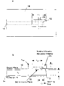
Referring now to Figs. 1 a and 1 b, a slot-fed rectangular dielectric
resonator antenna is
shown with the centre portion removed, forming a rectangular notch 12. The
antenna is
fabricated from medium to high dielectric constant material disposed on a
ground
metalized substrate. The bottom layer of the substrate is a microstrip line
feed layer 14. A
signal is coupled to the antenna through a narrow rectangular slot 16,
perpendicular to the
feed line, in the common ground plane 18 between the antenna and the
microstrip line 14.
In operation, the antenna behaves like a short magnetic dipole aligned along
the axis of
the slot 16 with the maximum radiation in the boresight direction. In
instances where the
efficiency of coupling is low, the coupling efficiency can be improved by
increasing the
magnetic field intensity arvound the slot through the use of a thin strip 23
of high dielectric
constant shown in Fig. 2a. In Fig. 2a a high dielectric constant insert 23
placed over the
slot 16 in the central portion of a rectangular DRA 24 thereby being disposed
between the
feed means and the; dielectric resonator, is first coupled thus creating a
strong magnetic
field in its vicinity. This in turn strongly excites the required mode of the
rectangular
DRA 24. It is preferable that the high dielectric constant substrate 22 or
insert 23 has a
dielectric value of at least twice that of the DRA 24, and in a preferred
embodiment, the
value of the dielectric constant of the substrate 22 has shown in Fig. 2b), or
insert 23, is 4
times that of the DRA 24. It is :further preferred that high dielectric 22 or
23 be
substantially non-rf;sonant at a resc,~nance of the first dielectric
resonator; it serves to
concentrate the field in to upper dielectric resonator and to match the feed
to the
resonator. The dimension of the thin high dielectric constant strip 23 is
experimentally
optimized. The dielectric strip i;> much thinner than the DRA so that the
major
contribution to the radiation is from the DRA. Preferably the thickness of the
dielectric
substrate 22 is less than n,/10. The high dielectric strip can also be used to
enhance the
coupling to the DRA from a microstrip line 14 as well as a slot 16, as shown
in Fig. 2b.
Fig. 2c shown an embodiment similar to that of Fig 2a, wherein a high
dielectric insert
material 23 fills the; entire notched portion or cavity defined within the
DRA. Also, the
6
CA 02201048 2001-06-07
Doc. No 18-5 Patent
DRA need not have a notch, rectangular or otherwise, in order for the high
dielectric
constant insert to enhance the coupling. In Figs. 2b and 2d, the dielectric
resonator
antenna is shown having a mic.rostrip ground plane on the bottom face of a
substrate
having a microstrip feed line on top o:f the substrate. The high dielectric
insert layer 23 is
disposed between the microstrip ground plane and the solid DRA. The embodiment
shown in Fig. 2d includes a plurality of layers 23a and 23b of different
permittivities.
Experimental Results
Several notched DRAB of different L1/L2 ratios were fabricated from RT/Duroid
6010
with dielectric constant of 10.8. At present, the theory to determine the
resonant
frequency for this DRA structure is not yet known. Thus, their dimensions were
determined using the theory of a sc>lid rectangular DRA. From perturbation
theory, it was
expected that the resonant frequency of the notched DRA would be slightly
higher than
the solid rectangular DRA. This was confirmed by the measured results. It
should be
noted that the operating frequency in this study was arbitrarily chosen for
the
convenience of the measurement. In the following experiment, the slot
dimensions and
the matching stub length I~3 (shown in Fig. 1 b) were optimized so that one of
the samples
had a good match to the feed line. rClzis same slot was then used to feed the
other samples
so that the effects o:f Ll/Lz could be studied.
The measured return loss of notched DRAs having different ratios of L1/L2 is
shown in
Fig. 3. The results show the characteristic of a double tuned resonant
circuit. The ratio
L~/LZ can be used to control the location of the upper and the lower
resonating
frequencies, which increase with L~/ L2. When the two frequencies are located
closer to
each other, the antenna has a broad operating bandwidth. When the two
frequencies are
farther apart, the antenna can be utilized in a dual band mode of operation.
For the
samples studied, it is found that the bandwidth of the notched DRA can be
increased to
28% as compared to 10% for its solid counterpart. The measured radiation
patterns of this
antenna varied only slightly over this broad impedance bandwidth, (as shown in
Fig. 4).
Hence, it is clear that the operating bandwidth of this notched dielectric
antenna is 28%,
7
CA 02201048 2001-06-07
Doc. No 18-5 Patent
which is a significant improvement over its solid counterpart and the single
microstrip
patch element (a few per cent bandwidth). It should be noted that the cross-
polarization
level of this antenna is 20 dB lower than the peak co-polarization level over
the same
frequency band.
The DRAs above when redesignf:d for the operation at half of the original
operating
frequencies, were i:abricated from material with a dielectric constant of 10.
The feed line
was constructed from the same substrate as in the previous cases. Using the
above design
it was found that it was not possible to achieve the efficient coupling
without making the
slot size too big. This is not a desirable solution due to increasing
radiation loss from the
slot.
In accordance with this invention, by introducing a material with a high
dielectric
constant, in the farm of an insert (Fig. 2a), the coupling efficiency was
significantly
increased without increasing the radiation loss from the slot. The achieved
operational
bandwidth was found to be 30%.
Tests were also carried out using the configuration shown in Fig. 2b, where a
solid DRA
was placed on top of a microstrip Mine. Using a DRA of dielectric constant 10,
there was
only a limited amount of coupling; when the DRA was placed on a open-ended 50
S2
microstrip line, achieving a maxirrmm of 5 dB return loss. When a thin
dielectric insert
(dielectric constant of 40) was added (Fig. 2b), the amount of coupling
increased
substantially, achieving a maximum return loss of 24 dB and a 10 dB return
loss
bandwidth of 16% as shown in Fig 5. Thus there is significant improvement in
using a
thin dielectric insert having a higT;h dielectric constant between the feed
line and the
dielectric resonator.
In another embodiment of the invention, a high gain, low profile active phased
array
antenna is provided with electronic beam steering capability in the azimuth
plane. The
radiating elements comprise the nrulti-segment dielectric resonator antennas
described
heretofore optionally and preferably, of rectangular cross-section, and fed by
a microstrip
8
CA 02201048 2001-06-07
Doc. No 18-5 Patent
line. Providing the thin dielectric insert 22 having a high dielectric
constant, between the
feed line and the dielectric resonators enhances the operation of the DRAB.
The array combines DRA technology with mufti-layer printed technology and
offers
high gain, wide pattern bandwidths, and electronic beam steering capability.
Diagrams of the geometry of the array are shown in Figs. 6a and 6b. The array
has a
mufti-layer architecture having a radiating board 66, and feed distribution
board 68. The
radiating antenna includes 16 linear column arrays of mufti-segment DRA
elements 64.
Each linear column comprises two collinear sub-arrays formed of branched
microstrip
lines 63 feeding 10 DRA elements; the 10-element sub-array is shown in Figs 7a
and 7b.
These branched lines are in turn fed by aperture coupling to the power
distribution
network, located on a second layer beneath the radiating board. The power
distribution
network includes a printed corporate feed, incorporating phase shifters for
electronic
beam steering in the azimuth plane. Low noise amplifiers (LNAs) are also
integrated into
each column to reduce the adverse effects of transmission line loss with
respect to noise
temperature.
Several prototype arrays have beers fabricated and tested. The first array to
be fabricated
was a passive antenna containing fi4 elements. The next iteration, which has
recently
been completed and tested, was an active antenna containing 320 DRAs and 16
integrated
LNAs (15 dB gain stage). The measured patterns are shown in Figs. 8 and 9
while the
boresight gain versus normalized frequency is shown in Fig. 10. A peak active
gain
(antenna gain including LNAs) of 39 dBi was measured with a 3 dB gain
bandwidth of
15%. Good cross-polarization was also achieved, with levels on the order of 20
dB below
the peak co-polarizf:d gain on boresight.
Of course, numerous other embod:irnents may be envisaged without departing
from the
spirit and scope of the invention.
9