Note: Descriptions are shown in the official language in which they were submitted.
2201243
TITLE OF THE INVENTION
ELECTR,ON-BEAM GENERATING APPARATUS,
IMAGE DISPLAY APPARATUS HAVING THE SAME,
AND METHOD OF DRrVING THE~EOF
BACKGROUND OF THE INVENTION
The present invention relates to an electron-beam
generating apparatus having a multi-electron-beam source
in which a plurality of cold cathode devices are wired
in a matrix, an image display apparatus using the
electron-beam generating apparatus, and a method of
- driving these apparatuses.
Conventionally, two types of devices, namely
thermionic and cold cathode devices, are known as
electron-emitting devices. Examples of cold cathode
devices are surface-conduction electron-emitting devices,
field-emission-type devices (to be referred to as FE-
type devices hereinafter), and metal/insulator/metal
type emission devices (to be referred to as MIM-type
devices hereinafter).
A known example of the surface-conduction
electron-emitting devices is described in, e.g., M.I.
Elinson, Radio. Eng. Electron Phys., 10, 1290 (1965) and
other examples to be described later.
The surface-conduction electron-emitting device
utilizes the ph~n~m~no~ in which electron emission is
220 1 243
caused in a small-area thin film formed on a substrate,
by providing a current parallel to the film surface. The
surface-conduction electron-emitting device includes
devices using an Au thin film (G. Dittmer, "Thin Solid
Films", 9,317 (1972)), an In2O3/SnO2 thin film (M.
Hartwell and C.G. Fonstad, "IEEE Trans. ED Conf. n ~ 519
(1975)), and a carbon thin film (Hisashi Araki, et al.,
"Vacuum", Vol. 26, No. 1, p. 22 (1983)), and the like,
in addition to an SnO2 thin film according to Elinson
mentioned above.
Fig. 23 is a plan view of the surface-conduction
emitting device according to M. Hartwell et al. as a
typical example of the structures of these surface-
conduction electron-emitting devices. Referring to Fig.
23, reference numeral 3001 denotes a substrate; and 3004,
a conductive thin film made of metal oxide formed by
sputtering. This conductive thin film 3004 has an H-
shaped plane pattern, as shown in Fig. 23. An electron-
emitting portion 3005 is formed by performing an
electrification process (referred to as an energization
-forming process to be described later) with respect to
the conductive thin film 3004. Referring to Fig. 23, a
spacing L is set to 0.5 to 1 mm, and a width W is set to
0.1 mm. The electron-emitting portion 3005 is shown in a
rectangular shape at the center of the conductive thin
film 3004 for the sake of illustrative convenience,
2201 243
however, this does not exactly show the actual position
and shape of the electron-emitting portion.
In the above surface-conduction electron-emitting
device by M. Hartwell et al., typically the electron-
emitting portion 3005 is formed by performing theelectrification process called energization forming
process for the conductive thin film 3004 before
electron emission. According to the energization forming
process, electrification is performed by applying a
constant or varying DC voltage which increases at a very
slow rate of, e.g., 1 V/min, to both ends of the
. conductive thin film 3004, so as to partially destroy or
deform the conductive thin film 3004 or change the
properties of the conductive thin film 3004, thereby
forming the electron-emitting portion 3005 with an
electrically high resistance. Note that the destroyed or
deformed part of the conductive thin film 3004 or part
where the properties are changed has a fissure. Upon
application of an appropriate voltage to the conductive
thin film 3004 after the energization forming process,
electron emission occurs near the fissure.
Known examples of the FE-type devices are
described-in W.P. Dyke and W.W. Dolan, "Field Emissionn,
Advance in Electron Physics, 8,89 (1956) and C.A. Spindt,
"Physical properties of thin-film field emission
- cathodes with molybdenum cones~, J. Appl. Phys., 47,5248
220 1 243
(1976).
Fig. 24 is a cross-sectional view of the device
according to C.A. Spindt et al. as a typical example of
the construction of the FE-type devices. Referring to
Fig. 24, reference numeral 3010 denotes a substrate;
3011, an emitter wiring comprising an electrically
conductive material; 3012, an emitter cone; 3013, an
insulating layer; and 3014, a gate electrode. rrhe device
is caused to produce field emission from the tip of the
emitter cone 3012 by applying an appropriate voltage
across the emitter cone 3012 and gate electrode 3014.
In another example of the construction of an FE-
type device, the stacked structure of the kind shown in
Fig. 24 is not used. Rather, the emitter and gate
electrode are arranged on the substrate in a state
substantially parallel to the plane of the substrate.
A known example of the MIM-type is described by
C.A. Mead, "Operation of tunnel-emission devices", J.
Appl. Phys., 32, 646 (1961). Fig. 25 is a sectional view
illustrating a typical example of the construction of
the MlM-type device. Referring to Fig. 25, reference
numeral 3020 denotes a substrate; 3021, a lower
electrode consisting of metal; 3022, a thin insulating
layer having a thickness on the order of 100 A; and 3023,
an upper electrode consisting of metal and having a
thickness on the order of 80 to 300 A. The device is
220 1 243
caused to produce field emission from the surface of the
upper electrode 3023 by applying an appropriate voltage
across the upper electrode 3023 and lower electrode 3021.
Since the above-mentioned cold cathode device
makes it possible to obtain electron emission at a lower
temperature in comparison with a th~rm;onic cathode
device, a heater for applying heat is unnecessary.
Accordingly, the structure is simpler than that of the
thermionic cathode device and it is possible to
fabricate devices that are finer. Further, even though a
large number of devices are arranged on a substrate at a
. high density, problems such as fusing of the substrate
- do not easily occur. In addition, the cold cathode
device differs from the therm; onic cathode device in
that the latter has a slow response because it is
operated by heat produced by a heater. Thus, an
advantage of the cold cathode device is the quicker
response.
For these reasons, extensive research into
applications for cold cathode devices is being carried
out.
By way of example, among the various cold cathode
devices, the surface-conduction electron-emitting device
is particularly simple in structure and easy to
manufacture and therefore is advantageous in that a
large number of devices can be formed over a large area.
2201 243
Accordingly, research has been directed to a method of
arraying and driving a large number of the devices, as
disclosed in Japanese Patent Application Laid-Open No.
64-31332, filed by the present applicant.
Further, applications of surface-conduction
electron-emitting devices that have been researched are
image forming apparatuses such as an image display
apparatus and an image recording apparatus, charged beam
sources, and the like.
As for applications to image display apparatus,
research has been conducted with regard to such an image
. display apparatus using, in combination, surface-
conduction electron-emitting devices and phosphors which
emit light in response to irradiation with electron beam,
as disclosed, for example, in the specifications of USP
5,066,883 and Japanese Patent Application Laid-Open
(KOKAI) Nos. 2-257551 and 4-28137 filed by the present
applicant. The image display apparatus using the
combination of the surface-co~l]ction electron-emitting
devices and phosphors is expected to have
characteristics superior to those of the conventional
image display apparatus of other types. For ex-ample, in
c~mp~rison with a liquid-crystal display apparatus that
have become so popular in recent years, the above-
mentioned image display apparatus is superior since it
emits its own light and therefore does not require back-
2201 243
lighting. It also has a wider viewing angle.
A method of,driving a number of FE-type devices in
a row is disclosed, for example, in the specification of
USP 4,904,895 ~iled by the present applicant. A flat-
type display apparatus reported by R. Meyer et al., forexample, is known as an example of an application of an
FE-type device to an image display apparatus. [R. Meyer:
~Recent Development on Microtips Display at LETI", Tech.
Digest of 4th Int. Vacuum Microelectronics Conf.,
Nagahama, pp. 6 ~ 9, (1991).]
An example in which a number of MIM-type devices
-- are arrayed in a row and applied to an image display
apparatus is disclosed in the specification of Japanese
Patent Application Laid-Open No. 3-55738 filed by the
present applicant.
The present inventors have examined electron-
emitting devices according to various materials,
manufacturing methods, and structures, in addition to
the above conventional devices. The present inventors
have also studied a multi-electron-beam source in which
a large number of electron-emitting devices are arranged,
and an image display apparatus to which this multi-
electron source is applied.
The present inventors have also examined a multi-
electron-beam source according to an electric wiring
method shown in Fig. 26. More specifically, this multi-
2201 243
electron-beam source is constituted by two-dimensionally
arranging a larg~ number of electron-emitting devices
and wiring these devices in a matrix, as shown in Fig.
26.
Referring to Fig. 26, reference numeral 4001
denotes an electron-emitting device; 4002, a row wiring;
and 4003, a column wiring. In reality, the row wiring
4002 and the column wiring 4003 include limited
electrical resistance; yet, in Fig. 26, they are
represented as wiring resistances 4004 and 4005. The
wiring shown in Fig. 26 is referred to as simple matrix
~- wiring.
For the illustràtive convenience, the multi-
electron-beam source constituted by a 6X6 matrix is
shown in Fig. 26. However, the scale of the matrix is
not limited to this arrangement. In a multi-electron-
beam source for an image display apparatus, a number of
devices sufficient to perform desired image display are
arranged and wired.
In the multi-electron-beam source in which the
electron-emitting devices are wired in a simple matrix,
appropriate electrical signals are supplied to the row
wiring 4002 and the column wiring 4003 to output desired
electron beams. For instance, when the electron-emitting
devices of one arbitrary row in the matrix are to be
driven, a selection voltage Vs is applied to the row
2201 243
wiring 4002 of the selected row. Simultaneously, a non-
selection voltage V~ is applied to the row wiring 4002
of unselected rows. In synchronization with this
operation, a driving voltage Ve for outputting electron
beams is applied to the column wiring 4003. According to
this method, a voltage (Ve - V8) is applied to the
electron-emitting devices of the selected row, and a
voltage (Ve - V~) is applied to the electron-emitting
devices of the unselected rows, assuming that a voltage
drop caused by the wiring resistances 4004 and 4005 is
negligible. When the voltages Ve, Vs~ and V~ are set to
appropriate levels, electron beams with a desired
intensity are output from only the electron-emitting
devices of the selected row. When different levels of
driving voltages Ve are applied to the respective column
wiring 4003, electron beams with different intensities
are output from the respective devices of the selected
row. Since the response rate of the cold cathode device
is fast, the period of time over which electron beams
are output can also be changed in accordance with the
period of time for applying the driving voltage Ve.
Accordingly, the multi-electron-beam source having
electron-emitting devices arranged in a simple matrix
can be used in a variety of applications. For example,
the multi-electron-beam source can be suitably used as
an electron source for an image display apparatus by
220 1 243
appropriately supplying a voltage signal according to
image data.
However, when a voltage source is actually
connected to the multi-electron-beam source and the
multi-electron-beam source is driven in the above
described method of voltage application, a problem
arises in that the voltage practically supplied to each
of the electron-emitting devices is varied since the
voltage drops due to wiring resistance.
A primary cause of such variance in the voltage
applied to each of the devices is the difference in
. wiring lengths for each of the electron-emitting devices
wired in a simple matrix (i.e. magnitudes of wiring
resistances are different for each of the devices).
The second cause is the non-uniform voltage drop
caused by the wiring resistance 4004 in respective
portions of the row wiring. Since the current flowing
from the row wiring of the selected row is diverged to
each of the electron-emitting devices connected to the
selected row, levels of the current provided to each of
the wiring resistances 4004 are not uniform, causing the
aforementioned non-uniformity.
The third cause is in that the level of voltage
drop caused by the wiring resistance varies depending on
a driving pattern (an image pattern to be displayed).
This is because the current provided to the wiring
-- 10 --
2201 243
resistance changes in accordance with a driving pattern.
- Due to the aforementioned causes, the voltage
applied to each of the electron-emitting devices varies.
Therefore, an intensity of electron beam outputted from
each of the electron-emitting devices deviates from a
desired value, causing a problem in applications. For
instance, in a case where the above-described method is
applied to an image display apparatus, lllm;n~nce of a
displayed image becomes non-uniform, or the lllm;nAnce
changes dep~n~; ng on a displayed image pattern.
Furthermore, since the variance of voltage tends
to be greater as the scale of the simple matrix becomes
large, the number of pixels in the image display
apparatus has to be limited.
In view of the above problems, the present
inventors have conducted extensive studies and have
experimented a driving method different from the
aforementioned voltage application method.
More specifically, according to the experimented
method, upon driving multi-electron-beam source in which
the electron-emitting devices are wired in a simple
matrix, instead of connecting the voltage source with
the column wiring to apply the driving voltage Ve, a
current source is connected to supply a current
necessary to output desired electron beams. In this
method, the level of emission current Ie is controlled by
2201 243
controlling the level of device current If.
In other words, the level of device current If to
be provided to each electron-emitting device is
determined by referring to a characteristic representing
(device current If) vs. (emission current Ie) of the
electron-emitting device, and the determined level of
the device current If is supplied by the current source
connected to the row wiring. More specifically, the
driving circuit is constructed by combining electric
circuits such as a memory storing the characteristic
representing (device current If) vs. (emission current
Ie)~ a calculator for determ;n;ng the device current If
to be provided, a controlled current source and the like.
The controlled current source of the driving circuit may
employ a form of a circuit in which the level of the
device current If to be provided is first converted to a
voltage signal and then to current by a voltage/current
converter.
According to the above method, as compared with
the foregoing driving method of connecting a voltage
source, it is less likely to be influenced by voltage
drop due to the wiring resistance. Therefore, the above
method provides a considerable effect to m;n;m;ze the
variance and change in intensity of output electron
beams (EPA 688 035).
However, the driving method of connecting a
- 12 -
2201 243
current source still raises the following problems.
That is, in a case where a constant current pulse
having a short time-width is supplied from a controlled
constant current source to the multi-electron-beam
source in which a considerably large number of electron-
emitting devices are wired in a matrix, electron-beam is
hardly emitted. If the constant current pulse is
continuously supplied for a relatively long period of
time, electron-beams are emitted as a matter of course;
however a long start-up time is necessary to start the
electron emission.
. Figs. 22B - 22E are time charts for expl~;n;ng the
above. Fig. 22B is a graph showing t;m;ng for sc~nn;ng
the row wiring; Fig. 22C, a graph showing a current
waveform output from the controlled constant current
source; Fig. 22D, a graph showing the driving current
practically provided to the electron-emitting devices;
and Fig. 22E, a graph showing the intensity of electron
beam emitted from the electron-emitting devices. As can
bè seen from these figures, when a short current pulse
is supplied from the controlled constant current source,
device current If is not provided to the electron-
emitting devices. If a iong current pulse is supplied,
the driving current provided to the electron-emitting
devices has a waveform with a large rise-time.
Although a cold cathode type electron-emitting
2201 243
device has a characteristic of fast response, since the
current waveform ~has a long rise time, the resulting
waveform of the emission current Ie is also deformed.
The foregoing problems arise due to the following
reasons. In a multi-electron-beam source where electron-
emitting devices are wired in a simple matrix, parasitic
capacity increases as the scale of the matrix is
enlarged. The parasitic capacity is mainly present where
the row wiring and column wiring intersect. An
equivalent circuit thereof is shown in Fig. 22A. When a
controlled constant current source 11 connected to a
- column wiring 54 starts supplying a constant current Il,
the supplied current is first consumed to charge
parasitic capacity 48 before the supplied current serves
as a driving current for electron-emitting devices 41.
Thus, the practical response speed of the electron-
emitting devices is reduced.
More specifically, to attain practical light
emission lllm;n~nce in a display apparatus having cold
cathode devices and phosphors, it is necessary to supply,
generally speaking, at least 1 ~A to 10 mA of driving
current, to a cold cathode device corresponding to one
pixel. If a driving current larger than necessary is
supplied, a problem arises in that the life of the cold
cathode devices is shortened.
To cope with the above problems, an output current
- 14 -
2201 243
of the controlled constant current source is controlled
to an appropriate value ranging from 1 ~A to 1 mA. (In
reality, the most appropriate value of driving current
is determined in consideration of the type, material,
and the form of the cold cathode, or efficiency of light
emission and an acceleration voltage of the phosphors.)
Me~nwh; le, in order to serve as a practical
television set or a computer display, it is preferable
to have, e.g. the number of pixels of a display screen
more than 500X500 and a screen whose diagonal size
larger than 15 ;nches. If the matrix wiring is to be
.- formed by utilizing a general technique of deposition,
wiring resistance E and parasitic capacity c are
produced, as has been described above. The circuit has a
charging time constant Tc which depends upon the
magnitude of E and _. (Strictly speaking, the time
constant of the circuit also depends upon plural
parameters, as a matter of course.)
In the case of driving the electron-emitting
devices with the voltage source, the response speed of
the electron-emitting devices which are connected in
parallel to the parasitic capacity depends upon the time
constant Tc.
However, in a case where a constant current
ranging from 1 ~A to 1 mA is supplied by the controlled
current source as described above, the time necessary
2201 243
for charging is even longer than the above time constant
Tc. In other wor~s, the practical response speed of the
electron-emitting devices is slower than that in the
case of driving by a voltage source.
Accordingly, in a case where light emission
lllm;n~nce in a display apparatus is controlled by the
pulse-width modulating method, linea~ity of a grayscale
in a low lllm;n~nce portion is deteriorated. Moreover,
when an image moving in quick motion is displayed, a
viewer receives an unnatural image.
As described above, in the case where a
modulated signal is supplied by a controlled constant
current source, the influence of voltage drop due to
wiring resistance is greatly improved. However, the
practical response speed is reduced, resulting in
deteriorated quality of a displayed image. If an area of
a display screen is enlarged or the number of pixels in
the display screen is increased, the parasitic capacity
is increased, thus the above problem has become more
evident.
SUMMARY OF ~1~ INVENTION
The present invention has been made in
consideration of the above situation, and has as its
object to provide driving means and a driving method for
uniformly outputting electron-beam at high speed from a
- 16 -
220 1 243
multi-electron-beam source comprising a large number of
electron-emittlng devices wired in a matrix. Another
object of the present invention is to provide a display
apparatus which has no lllm;n~nce unevenness, and
realizes superior linearity of a grayscale and has a
characteristic of quick response.
In order to attain the above objects, according to
the present invention, an electron-beam generating
apparatus, having a multi-electron-beam source where a
plurality of cold cathode devices are wired with row
wiring and column wiring arranged in a matrix form,
-~ sc~nn;ng means connected to the row wiring, and
modulation means connected to the column wiring, is
characterized in that the modulation means comprises: a
controlled current source for supplying a driving
current pulse to the cold cathode devices; a voltage
source for charging parasitic capacity of the multi-
electron-beam source at high speed; and a charging-
voltage apply means for electrically connecting the
voltage source and the colum.n wiring in synchronization
with a rise of the driving current pulse.
Herein, the charging-voltage apply means is
preferably the means including a rectifier or means
including a timer circuit and a connection switch.
Furth~rmore, the voltage outputted by the voltage
source is within a range of 0.5 - 0.9 times the maximum
2201 243
potential generated by the controlled current source.
Moreover, the electron-beam generating apparatus
is characterized in that the voltage source is a
variable voltage source capable of adjusting an output
voltage.
FurthermQre, the controlled current source
preferably includes a constant current circuit and a
current switch, or a V/I conversion circuit.
Furthermore, the charging-voltage apply means is
preferably a level shift circuit where a plurality of
diodes or transistors are connected.
. The electron-beam generating apparatus according
to the present invention constitutes an image display
apparatus if combined with image forming members which
form an image by irradiating electron beam generated by
the above-mentioned electron-beam generating apparatus.
The present invention also includes this image display
apparatus.
Moreover, the present invention includes a driving
method of an electron-beam generating apparatus having a
multi-electron-beam source where a plurality of cold
cathode devices are wired with row wiring and column
- wiring arranged in a matrix form, wherein a driving
current pulse, modulated in accordance with modulation
data inputted from an external unit, is supplied to the
column wiring, and a charging voltage is applied to the
- 18 -
2201 243
column wiring in addition to the driving current pulse
during a period from a rise of the driving current pulse
until a point at which parasitic capacity of the multi-
electron-beam source is charged to a predetermined level.
Still further, the present invention includes a
driving method of an image display apparatus having a
multi-electron-beam source where a plurality of cold
cathode devices are wired with row wiring and column
wiring arranged in a matrix form, wherein a driving
current pulse, modulated in accordance with modulation
data inputted from an external unit, is supplied to the
- column wiring, and a charging voltage is applied to the
column wiring in addition to the driving current pulse
during a period from a rise of the driving current pulse
until a point at which parasitic capacity of the multi-
electron-beam source is charged to a predetermined level.
According to the present invention, in order to
drive a multi-electron-beam source in which cold cathode
devices are wired in a matrix, a voltage for quickly
charging parasitic capacity is applied by a charging-
voltage apply circuit in addition to a driving current
being supplied from a controlled current source. By
virtue of the above, it is possible for electron-
emitting devices to respond fast. After the parasitic
capacity is charged, the charging-voltage apply circuit
is turned off, and the electron-emitting devices are
-- 19 --
2201 243
driven by the controlled current source. Therefore, the
cold cathode devi,ces can be driven quickly, without
being influenced by wiring resistance. Accordingly, an
image display apparatus applying the present invention
has superior linearity of a grayscale. Also, a viewer
receives a natural image when a moving-image is
displayed. Particularly, since the present invention
enables quick charging of parasitic capacity in a
display apparatus having a large display screen, an
image can be displayed with high quality.
Other features and advantages of the present
-~ invention will be apparent from the following
description taken in conjunction with the accompanying
drawings, in which like reference characters designate
the same or similar parts throughout the figures thereof.
BRIEF DESCRIPTION OF THE DRAWINGS
The accompanying drawings, which are incorporated
in and constitute a part of the specification,
illustrate embodiments of the invention and, together
with the description, serve to explain the principles of
the invention.
Fig. 1 is a block diagram showing a general
construction of the present invention;
Figs. 2A-2D show a charging-voltage apply circuit;
Fig. 3 shows a sc~nn;ng circuit;
- 20 -
220 1 243
Fig. 4 is a circuit diagram according to the first
embodiment;
Figs. 5A-5H are time charts for expl~;n;ng a
driving method according to the first embodiment;
Figs. 6A and 6B are circuit diagrams including a
voltage source and a charging-voltage apply circuit;
- Fig. 7 is a circuit diagram according to the
second embodiment;
Figs. 8A and 8B are circuit diagrams including a
voltage source and a charging-voltage apply circuit;
Fig. 9 is a circuit diagram according to the third
embodiment,
Figs. lOA and lOB are diagrams for explaining a
V/I converter utilized in the third embodiment;
Fig. 11 is a perspective view showing an image
display apparatus according to the present embodiment
where a part of the display panel is cut away;
Figs. 12A and 12B a plan views exemplifying an
arrangement of phosphors used in a face plate of a
display panel;
Fig. 13A - iS a plan view of a plane type surface-
conduction electron-emitting device utilized in the
present embodiment;
Fig. 13B iS a sectional view of the plane type
surface-conduction electron-emitting device utilized in
the present embodiment;
220 1 243
Figs. 14A to 14E are sectional views showing steps
of manufacturing ,the plane type surface-conduction
electron-emitting device;
Fig. 15 is a graph showing a waveform of applied
voltage in an energization forming process;
Fig. 16A is a graph showing a waveform of applied
voltage in an activation process;
Fig. 16B is a graph showing a variance of emission
current Ie;
Fig. 17 is a sectional view of a step-type
surface-conduction electron-emitting device utilized in
the present embodiment;
Fig. 18 is a graph showing a typical
characteristic of the surface-conduction electron-
emitting device utilized in the present embodiment;
Figs. l9A-19F are cross sectional views showing
steps of manufacturing the step-type surface-conduction
electron-emitting device;
Fig. 20 is a plan view of a substrate of a multi-
electron-beam source utilized in the present embodiment;
Fig. 21 is a partial cross sectional view of the
substrate of the multi-electron-beam source utilized in
the present embodiment;
Figs. 22A-22E are a diagram and graphs for
expl~;n;ng the conventional driving method and
exemplifying problems thereof;
- 22 -
2201 243
Fig. 23 shows a conventional surface-conduction
electron-emitting device;
Fig. 24 shows a conventional FE-type device;
Fig. 25 shows a conventional MIM-type device; and
Fig. 26 is a view showing a method of wiring in a
simple matrix.
DETAILED DESCRIPTION OF THE PREFERRED EMBODIMENTS
Preferred embodiments of the present invention
will be described in detail in accordance with the
accompanying drawings.
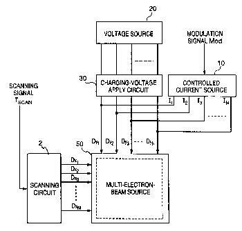
Fig. 1 is a block diagram showing a general
construction of driving means according to the present
invention. Referring to Fig. 1, reference numeral 10
denotes a controlled current source; 20, a voltage
source; 30, a charging-voltage apply circuit; 2, a
sc~nn; ng circuit; and 50, a multi-electron-beam source.
Hereinafter, each of the units will be described in
detail.
As has been explained above, the multi-electron-
beam source 50 includes MXN number of cold cathode
devices in which M number of row wiring and N nl]mh~r of
column wiring are arranged in a matrix. Each of the row
wiring is electrically connected to the sc~nn;ng circuit
2 via connection t~rm;n~ls ~xl to Dx~. Each of the
column wiring is electrically connected to the
- 23 -
2201 243
controlled current source 10 and charging-voltage apply
circuit 30 via co,nnection term;nAls Dyl to DYN
The controlled current source 10 outputs current
signals (Il to IN), modulated on the basis of a
modulation signal Mod, to the multi-electron-beam source
50. A so-called V/I converter may be utilized as the
controlled current source; more specifically, it is
preferable to utilize a circuit employing reference
numerals 11, 22 and 33 in Fig. 4 or a current mirror
circuit shown in Fig. lOB.
The voltage source 20 is used for charging
- parasitic capacity existing in the multi-electron-beam
source 50 in a short period of time. More specifically,
a DC constant voltage source or a pulse voltage source
may be utilized. It is even more preferable to utilize a
variable voltage source so that the charging voltage is
adjustable.
The charging-voltage apply circuit 30 is used for
electrically connecting the voltage source 20 and
connection term;nAls Dyl to ~y~ only for a period of time
necessary for charging the parasitic capacity. For
example, a rectifier circuit such as that shown in Figs.
2A or 2B, or a timer switch circuit where a timer 3Oa
and a connection switch 30b are combined as shown in Fig.
2C may be utilized. The rectifier circuit is
particularly preferable since it provides an advantage
- 24 -
- 2201 243
such that the voltage source and connection t~rm;n~ls
are smoothly disconnected (i.e. no noise is generated)
upon completing charging of the parasitic capacity. Note
that if diode or transistors are connected in series in
a plurality of steps, it is possible to alter the
charging voltage in accordance with the number of steps
connected (a level shift function). In addition, even
smoother charging is possible by providing a plurality
of rectifier circuits having different shift voltages in
parallel, as shown in Fig. 2D.
The sc~nn;ng circuit 2 is utilized to sequentially
apply a selection voltage V8 and a non-selection voltage
Vn8 to the row wiring of the multi-electron-beam source
50 in accordance with a sc~nn; ng signal T~. For
instance, a circuit as shown in Fig. 3 may be utilized.
The driving method according to the present
invention will be described next. When an arbitrary
electron-emitting device in the multi-electron-beam
source 50 is to be driven, the current pulse I is
outputted from the controlled current source 10 to the
column wiring of the multi-electron-beam source 50 in
accor~nce with the modulation signal Mod. In
synchronization with a rise of the current pulse, a
charging voltage is applied from the charging-voltage
apply circuit 30. When charging of the parasitic
capacity is almost completed, the voltage application
220 1 243
from the charging-voltage apply circuit 30 is stopped,
thereafter driving current is supplied from the
controlled current source 10 to the electron-emitting
device. According to the above driving method, charging
of the parasitic capacity is performed by the
cooperation of both the controlled current source and
the charging-voltage apply circuit 30, thus the charging
is completed in a short period of time. Upon completing
charging of the parasitic capacity, the charging-voltage
apply circuit 30 is turned off, and the controlled
current source 10 controls the driving current of the
.- electron-emitting device. Accordingly, it is possible to
realize a driving method which achieves quick response,
and which is not likely to be influenced by voltage drop
due to wiring resistance.
[First Embodiment]
The first embodiment applies the present invention
to a display apparatus having a multi-electron-beam
source. Fig. 4 is a block diagram showing a circuit
structure of the embodiment. In Fig. 4, reference
numeral 1 denotes a display panel including the multi-
electron-beam source. Reference letters Dxl to Dx~
denote connection t~rm;n~ls for row wiring of the multi-
electron-beam source; DY1 to DYN' connection term;n~ls
for column wiring of the multi-electron-beam source; Hv,
a high-voltage t~rm;nAl for applying an acceleration
- 26 -
2201 243
voltage to phosphors; and Va, a high-voltage source for
applying an acceleration voltage. Reference numeral 2
denotes a sc~nn; n~ circuit; 3, a synchronization signal
separation circuit; 4, a timing generation circuit; 5, a
shift register corresponding to one-sc~nn; ng line of
image data; 6, a line memory for storing the one line of
image data; 8, a pulse-width mo,dulator; 11, a constant
current circuit; 21, a voltage amplifier; 22, an
inverter; 31, a rectifier; and 33, a current switch
utilizing p-channel MOS-FET.
The construction and manufacturing method of the
- display panel 1 and the construction, manufacturing
method and characteristic of the multi-electron-beam
source included therein will be described later in
detail.
The correspondence of respective component in Fig.
4 and that shown in Fig. 1 is as follows: the voltage
amplifier 21 corresponds to the voltage source 20; the
rectifier 31 corresponds to the charging-voltage apply
circuit 30; and combination of the constant current
circuit 11 and the current switch 33 and the inverter 22
corresponds to the controlled current source 10.
The voltage amplifier 21 is constructed with an
operational amplifier. The rectifier 31 utilizes diode
shown in Fig. 2A. The constant current circuit 11 is
constructed with a constant voltage source and a current
- 27 -
2201 243
mirror circuit.
The present embodiment is a display apparatus
which displays a television signal utilizing the NTSC
scheme, therefore, the embodiment is operated on the
basis of an NTSC composite signal inputted from an
external unit. The synchronization signal separation
circuit 3 separates the NTSC composite signal into image
data DATA and a synchronization signal TsD~. The
synchronization signal TsD~ includes a vertical
synchronizing signal and a horizontal synchronizing
signal. The t;m;ng generation circuit 4 determines
. operation timing for each of the units on the basis of
these signals. More specifically, the t;m;ng generation
circuit 4 generates signals such as Ts~ which controls
operation t;m;ng of the shift register 5, T~y which
controls operation t; m;ng of the line memory 6, Ts~
which controls operation of the sc~nn;ng circuit 2, and
the like.
The im~ge data separated by the synchronization
signal separation circuit 3 is subjected to
serial/parallel conversion by the shift register 5, and
stored in the line memory 6 for a period of one
horizontal sc~nn;ng. The pulse-width modulator 8 outputs
a voltage signal obt~;ne~ by performing pulse-width
modulation on the image data stored in the line memory 6.
The voltage signal is supplied to the voltage
- 28 -
2201 243
amplifier 21 and inverter 22. The voltage amplifier 21
amplifies the voltage signal up to a level of charging
voltage. The inverter 22 inverses the voltage signal and
supplies it to the gate of the current switch 33.
The sc~nn; ng circuit 2 outputs the selection
voltage V8 or non-selection voltage V~ to the connection
t~rm; n~l S Dxl to D~ in order to sequentially scanning
respective rows of the multi-electron-beam source, and
includes M number of switches, e.g. as shown in Fig. 3.
Note that it is preferable to construct these switches
with transistors.
. It is preferable to determine the levels of the
selection voltage V8 and the non-selection voltage Vn8
outputted from the sc~nn;ng circuit 2, the level of
output current of the constant current circuit 11, a
sink voltage of the current switch 33 and an output
voltage of the voltage amplifier 21, on the basis of the
(applied device voltage Vf VS. emission current Ie)
characteristic and the (applied device voltage Vf VS.
device current If) characteristic of the cold cathode
devices to be utilized.
The multi-electron-beam source according to the
present embodiment includes surface-conduction electron-
emïtting devices having a characteristic shown in Fig.
18 which will be described later. Assume that the
surface-conduction electron-emitting device needs to
- 29 -
220 1 243
output 1.5 ~A of the emission current Ie in order to
achieve a desired lllm;n~nce in a display apparatus. In
this case, as can be seen from the graph in Fig. 18
showing the characteristic, it is necessary to provide
1.2 mA of the device current If to the surface-conduction
electron-emitting devices. Therefore, the output current
of the constant current circuit 11 is set at 1.2 mA. The
selection voltage Vs of the scAnn;ng circuit 2 is set at
-7 V; and the non-selection voltage V~, 0 V. If there
is no wiring resistance, the potential at the output
portion of the constant current circuit 11 should be 7 V.
(In order to provide 1.2 m~ of device current If, 14 V
must be provided at both ends of the device. Since the
selection voltage V~ is -7 V, the output potential of the
constant current circuit 11-should be 7 V.) However, in
practice, since there is a voltage drop in wiring, the
constant current circuit operates to compensate the
voltage drop. Therefore, in the case of utilizing this
multi-electron-beam source, the output potential may
increase to the m~;mllm level of 7.5 V (as a matter of
course, the maximum potential is subjected to change if
the wiring resistance changes). M~An-h;le, an electron
emission threshold voltage V~ of the surface-conduction
electron-emitting device is 8 V. Therefore, so long as
the non-selection voltage V~ is set at 0 V, electron-
beam is not emitted from the devices of unselected rows
- 30 -
2201 243
even when the output potential of the constant current
circuit 11 is increased to 7.5 V.
Furthermore, the sink potential of the current
, switch 33 is set at 0 V (ground potential) in the
embodiment shown in Fig. 3. Therefore, when the current
switch 33 is turned on, the potential of row wiring
becomes approximately 0 V, thus electron-beam is not
emitted from devices of the selected row or unselected
rows.
10Moreover, the output voltage of the voltage
amplifier 21 is set as follows. It is preferable to
. coincide the output voltage of the voltage amplifier 21
with the maximum output potential of the constant
current circuit 11, namely 7.5 V, in order to achieve
charging of the parasitic capacity at high speed.
However, it is safe to set the output voltage relatively
low considering the possibility of risk in the electron-
emitting device to which an excessive voltage may be
applied because of a variance in the circuit produced in
the course of manufacturing, or a variance in
characteristics of the circuit due to temperature change,
or a characteristic change in the circuit along with
passage of time, or generation of a ringing voltage due
to presence of parasitic inductance, or the like. In
practice, it is preferable to set the output voltage at
a value ranging between 0.5-0.9 times the maxLmum output
2201 243
potential of the current source. According to the
present embodiment, it-is designed such that the output
voltage is 6 V, considering the voltage drop in the
rectifier 31, with an assumption that voltage
amplification of the voltage amplifier 21 is 6/5 (see
Figs. 5B and 5C). Note that the voltage for charging the
parasitic capacity can be adjusted by changing the
amplification of the voltage amplifier 21 or the number
of steps of diodes, which is utilized in the rectifier
31, connected in series. Moreover, since the charging
speed depends upon the response speed of the voltage
amplifier, a waveform of the charging voltage can be
controlled by altering the response speed of the
amplifier. In addition, in a case where a DC voltage
source is utilized in place of the voltage amplifier 21,
it is preferable to set the output voltage relatively
lower than the electron emission threshold voltage V~ of
the electron-emitting device.
The operation of the circuit shown in Fig. 4 will
be described next with reference to the time chart shown
in Fig. 5. As has been described above, in the circuit
shown in Fig. 4, electron-emitting devices of the multi-
electron-beam source are selectively driven in the
sequence of each row, by the operation of the scanning
circuit 2. The graph in Fig. 5A shows a signal waveform
of a voltage supplied from the sc~nn; ng circuit 2 to the
2201 243
selected row wiring. Fig. 5B shows an example of a
signal waveform o~utputted from the pulse-width modulator
8. The pulse-width PW is changed in accordance with a
desired level of modulation. The voltage signal shown in
Fig. 5B is amplified by the voltage amplifier 21,
resulting in the waveform shown in Fig. 5C.
The voltage shown in Fig. 5C is applied to column
wiring via the rectifier 31. When the potential of
column wiring exceeds 6 V, the rectifier 31 operates in
a reversed polarity, thus is turned off. In other words,
parasitic capacity of the multi-electron-beam source is
quickly charged up to approximately 6 V by the voltage
applicatlon shown in Fig. 5C. The graph in Fig. 5E shows
a waveform of a current for charging the parasitic
capacity, supplied from the voltage amplifier 21.
Meanwhile, the waveform shown in Fig. 5B is
converted to an inverse phase by the inverter 22 to
control turning on/off of the current switch 33. As a
result, while the pulse-width modulation signal shown in
Fig. 5B is not supplied, the current switch 33 is turned
on, so that the current supplied from the constant
current circuit 11 is sunk to ground. Accordingly,
during this phase, the current outputted from the
constant current circuit 11 does not cause electron-beam
emission by the electron-emitting devices. The sink
current flowing to the current switch 33 is shown in the
2201 243
graph in Fig. 5F.
Accordingly~ the output current of the constant
current circuit 11 is supplied to the multi-electron-
beam source as a driving current while the current
switch 33 is turned off. In the present embodiment,
since the parasitic capacity is charged at high speed by
virtue of the voltage amplifier 21 as well as the
rectifier 31, the driving current is supplied
; mme~; ately to the electron-emitting devices. Fig. 5G
shows a waveform of current If provided to the electron-
emitting devices. Fig. 5H shows a waveform of electron-
beam output Ie emitted from the electron-emitting device.
Note that in Figs. 5G and 5H, the waveforms obtained in
the case of conventional driving circuit (i.e. not
including the voltage amplifier 21 and rectifier 31) is
indicated with broken lines for the purpose of
comparison.
According to the present embodiment, the practical
response speed of the multi-electron-beam source can be
improved as compared to the conventional method.
Therefore, according to the display apparatus of the
present emboA;m~nt, less unevenness in display lllm;n~nce
and a superior linearity of a grayscale are realized;
and even when a moving-image is displayed, a viewer
would not receive an unnatural image.
Note that the circuit shown in Figs. 6A or 6B may
220 1 243
be utilized in place of the rectifier 31 and voltage
amplifier 21. Mo,re specifically, Fig. 6A shows a circuit
combining a variable voltage source Vcc and a bipolar
transistor connected in the Darlington scheme. Herein,
resistance rS is connected between the base and the
ground in order to increase operation speed of the
transistor. Fig. 6B shows a circuit in which a MOS-FET
- is utilized instead of a bipolar transistor, whereby
providing an advantage of low manufacturing cost.
[Second Embodiment]
In the second embodiment of the present invention,
- - the direction of the driving current supplied to the
multi-electron-beam source is inverted from that of the
first embodiment. According to the second embodiment,
the constant current circuit for drawing current is
connected to the column wiring and an image signal is
subjected to pulse-width modulation. Fig. 7 shows a
circuit structure of the second embodiment. Reference
numeral 32 denotes a p-channel MOS transistors which
switch on/off the constant current (Il, I2, I3~ ~ ~ IN)
outputted from the constant current circuit 11 to be
provided to the column wiring. The pulse-width modulator
8 outputs pulse-width signals (PWl-PWN) to the voltage
amplifier (level shift circuit) 21 and the p-channel MOS
transistors 32. Only during the period within which the
pulse-width modulator 8 outputs a signal Lo-level, the
2201 243
transistors 32 brings the potential of column wiring
down to the GND a~d leads the output current (Il-IN) of
the constant current circuit 11 to the GND via the
transistors 32. Therefore, the potential of the column
wiring becomes 0 V during the period within which the
pulse-width modulator 8 outputs Lo-level. Meanwhile,
during the period within which the pulse-width modulator
8 outputs a signal Hi-level, the transistors 32 are
turned off, thus the output current (Il-IN) of the
constant current circuit 11 is provided to the electron-
emitting devices.
Note that in the second embodiment, the voltage
polarity of the voltage amplifier 21 and rectifier 31 is
reversed from that of the first embodiment. Therefore,
the rectifier 31 and the voltage amplifier 21 in the
present embodiment may be substituted with the circuits
shown in Figs. 8A and 8B. Fig. 8A shows a circuit
combining a variable voltage source Vss and a bipolar
transistor connected in the Darlington scheme. Herein,
resistance r~ is connected between the base and the
ground in order to increase operation speed of the
transistor. Fig. 8B shows a circuit in which a MOS-FET
is utilized instead of a bipolar transistor, whereby
providing an advantage of low manufacturing cost.
Similar to the first embodiment, the second
embodiment also achieves high-speed charging of the
- 36 -
2201 243
- parasitic capacity, realizing quicker response of the
electron-emitting~ devices as compared to the
conventional method.
In other words, according to the second embodiment,
the practical response speed of the multi-electron-beam
source can be improved as compared to the conventional
method. Therefore, according to a display apparatus of
the second embodiment, less unevenness in display
lllm;nAnce and a superior linearity of a grayscale are
realized; and even when a moving-image is displayed, a
viewer would not receive an unnatural image.
-- [Third Embodiment]
According to the third embodiment of the present
invention, a V/I conversion circuit is utilized as the
lS controlled current source 10 in Fig. 1. Fig. 9 shows a
circuit structure of the third embodiment. In Fig. 9,
reference numeral 12 denotes a V/I conversion circuit.
The V/I conversion circuit 12 includes N number of V/I
converters 14 as shown in Fig. lOA. It is preferable to
construct each of the V/I converters 14 with a current
mirror circuit as shown in Fig. lOB. The circuit
structure in Fig. 9 has an advantage of being suitable
for either of a puise-width modulation method or an
amplitude modulation method. Therefore, the same pulse-
width modulator used in the first embodiment may serveas a modulator 9, or an amplitude modulator may be
2201 243
utilized. The same voltage amplifier 21 and the
rectifier 31 as ~hat in the first embodiment are
utilized in the third embodiment.
Similar to the first embodiment, the third
embodiment also achieves high-speed charging of the
parasitic capacity, realizing quicker response of the
electron-emitting devices as compared to the
conventional method.
In other words, according to the third embodiment,
the practical response speed of the multi-electron-beam
source can be improved as compared to the conventional
method. Therefore, according to a display apparatus of
the third embodiment, less unevenness in display
lllm;n~nce and a superior linearity of a grayscale are
realized; and even when a moving-image is displayed, a
viewer would not receive an unnatural image.
<Arrangement and Manufacturing Method of Display Panel>
The arrangement and manufacturing method of the
display panel 1 of the image display apparatus according
to the first to third embodiments of the present
invention will be described below providing detailed
examples.
Fig. 11 is a partially cutaway perspective view of
a display panel used in the embodiments, showing the
internal structure of the panel.
Referring to Fig. 11, reference numeral 1005
- 38 -
220 1 243
denotes a rear plate; 1006, a side wall; and 1007, a
face plate. Thes,e parts 1005 to 1007 form an airtight
vessel for maintA;n;ng a vacuum in the display panel. To
construct the airtight vessel, it is necessary to seal-
connect the respective parts to allow their junctionportions to hold sufficient strength and airtight
condition. For example, frit glass is applied to the
junction portions and sintered at 400~C to 500~C in air
or a nitrogen atmosphere for 10 minutes or more, thereby
seal-connecting the parts. A method of evacuating the
airtight vessel will be described later.
-- The rear plate~ 1005 has a substrate 1001 fixed
thereon, on which N X M cold cathode devices 1002 are
formed. (N and M are positive integers of 2 or more and
appropriately set in accordance with a target number of
display pixels. For example, in a display apparatus for
high-definition television display, preferably N = 3,000
or more, and M = 1,000 or more. In this embodiment, N =
3,072, and M = 1,024.) The N X M cold cathode devices
are arranged in a simple matrix with M number of row
wiring 1003 and N number of column wiring 1004. The
portion constituted by the substrate 1001, the cold
cathode devices 1002, the row wiring 1003, and the
column wiring 1004 will be referred to as a multi-
electron-beam source. The manufacturing method and
structure of the multi-electron-beam source will be
- 39 -
220 1 243
described later in detail.
In this emb~odiment, the substrate 1001 of the
multi-electron-beam source is fixed to the rear plate
1005 of the airtight vessel. However, if the substrate
1001 of the multi-electron-beam source has a sufficient
strength, the substrate 1001 itself of the multi-
electron-beam source may be used as the rear plate of
the airtight vessel.
Furthermore, a phosphor film 1008 is formed on the
lower surface of the face plate 1007. As the display
panel of the present embodiment is a color display panel,
-- the phosphor film 1008 is coated with red (R), green (G),
and blue (B) phosphors, i.e., three primary color
phosphors used in the CRT field. As shown in Fig. 12A,
the R, G, and B phosphors are applied in a striped
arrangement. A black conductive material 1010 is
provided between the stripes of the phosphors. The
purpose of providing the black conductive material 1010
is to prevent display color misregistration even if the
electron beam irradiation position is shifted to some
extent, to prevent degradation of display contrast by
shutting off reflection of external light, to prevent
charge-up of the phosphor film 1008 by electron beams,
and the like. The black conductive material 1010 m~;nly
consists of graphite, though any other material may be
used as long as the above purpose can be attained.
- 40 -
220 1 243
The arrangement of the phosphors of the three
primary colors, i.e., R, G, and B is not limited to the
striped arrangement shown in Fig. 12A. For example, a
delta arrangement shown in Fig. 12B or other
arrangements may be employed.
When a monochromatic display panel is to be formed,
a monochromatic phosphor material must be used for the
phosphor film 1008. In this case, -the black conductive
material 1010 need not always be used.
Furthermore, a metal back 1009, which is well-
known in the CRT field, is provided on the rear plate
side surface of the phosphor film 1008. The purpose of
providing the metal back 1009 is to improve the light-
utilization ratio by mirror-reflecting part of light
emitted from the phosphor film 1008, to protect the
phosphor film 1008 from collision with negative ions, or
to use the metal back 1009 as an electrode for applying
an electron beam accelerating voltage, or to use the
metal back 1009 as a conductive path of electrons which
excited the phosphor film 1008, and the like. The metal
back 1009 is formed by forming the phosphor film 1008 on
the face plate 1007, applying a smoothing process to the
phosphor film surface, and depositing all~m;nllm (Al)
thereon by vacuum deposition. Note that when a phosphor
material for a low voltage is used for the phosphor film
1008, the metal back 1009 is not used.
- 41 -
2201 243
Furthermore, although not utilized in the above-
described embodiments, transparent electrodes made of,
e.g., ITO may be provided between the face plate 1007
and the phosphor film 1008, for application of an
accelerating voltage or for improving the conductivity
of the phosphor film.
Moreover, referring to Fig. 11, reference symbols
Dxl to D~, Dyl to DYN' and Hv denote electric connection
term;n~l~ for an airtight structure provided to
electrically connect the display panel to an electric
circuit (not shown). The term;n~ls Dxl to D~ are
electrically connected to the row wiring 1003 of the
multi-electron-beam source; the term;n~ls Dyl to ~YN~ to
the column wiring 1004 of the multi-electron-beam
source; and the term;n~l Hv, to the metal back 1009 of
- the face plate 1007.
In order to evacuate ~he interior of the airtight
vessel, an exhaust pipe and a vacuum pump, not shown,
are connected after the airtight vessel is assembled and
the interior of the vessel is exhausted to a vacuum of
10-7 Torr. The exhaust pipe is then sealed. In order to
maintain the degree of vacuum within the airtight vessel,
a getter film (not shown) is formed at a prescribed
position inside the airtight vessel ;mme~;~tely before
or ;mme~;~tely after the pipe is sealed. The getter film
is a film formed by heating a getter material, the main
- 42 -
2201 243
ingredient of which is Ba, for example, by a heater or
high-frequency heating to deposit the material. A vacuum
on the order of lX10-5 to lX10-7 Torr is maintained
inside the airtight vessel by the adsorbing action of
the getter film.
The foregoing descriptions have been provided with
respect to the arrangement and manufacturing method of
the display panel according to the present embodiments.
A method of manufacturing the multi-electron-beam
source 50 used in the display panel of the above-
described embodiments will be described next. If the
. multi-electron-beam source used in the image display
apparatus of this invention is an electron source having
cold cathode devices wired in a simple matrix, there is
no limitation upon the material, shape or method of
manufacturing of the cold cathode devices. Accordingly,
it is possible to use cold cathode devices such as
surface-conduction electron-emitting devices or cold
cathode devices of the FE or MIM-type.
- 20 Since there is ~mAn~ for inexpensive display
devices having a large display screen, the surface-
conduction electron-emitting devices are particularly
preferred as the cold cathode devices. More specifically,
with the FE-type device, the relative positions of the
emitter cone and gate electrode and the shape thereof
greatly influence the electron emission characteristics.
- 43 -
22~1 243
Consequently, a highly precise manufacturing technique
is required. This~ is a disadvantage in terms of
enlarging surface area and reducing the manufacturing
cost. With the MIM-type device, it is required that the
insulating layer and film thickness of the upper
electrode be made uniformly even if they are thin. This
also is a disadvantage in terms of enlarging surface
area and lowering the cost of manufacture. In this
respect, the surface-conduction electron-emitting device
is comparatively simple to manufacture, the surface area
thereof is easy to enlarge and the cost of manufacture
-- can be reduced with ease. Further, the inventors have
discovered that, among the surface-conduction electron-
emitting devices available, a device whose electron
emission portion or peripheral portion is formed from a
film of fine particles excels in its electron emission
characteristic, and that the device can be manufactured
easily. Accordingly, it may be construed that such a
device is most preferred for use in a multi-electron-
beam source of an image display apparatus having a highlllm;n~nce and a large display screen. Accordingly, the
display panel of the foregoing embodiments utilizes a
surface-conduction electron-emitting device whose
electron emission portion or peripheral portion was
formed from a film of fine particles. First, therefore,
the basic construction, method of manufacturing and
2201 243
characteristics of an ideal surface-conduction electron-
emitting device w,ill be described, and this will be
followed by a description of the structure of a multi-
electron-beam source in which a large number of devices
are wired in the form of a simple matrix.
<Preferred Structure and Manufacturing Method of
Surface-Conduction Electron-Emitting Device>
The typical structure of the surface-conduction
electron-emitting device, having an electron-emitting
portion or its peripheral portion made of a fine
particle film, includes a plane type structure and a
-- step type structure.
<Plane Type Surface-Conduction Electron-Emitting Device>
The structure and manufacturing method of a plane
type surface-conduction electron-emitting device will be
described first. Figs. 13A and 13B are plan and
sectional views for expl~;n;ng the structure of the
plane type surface-conduction electron-emitting device.
Referring to Figs. 13A and 13B, reference numeral 1101
denotes a substrate; 1102 and 1103, device electrodes;
1104, a conductive thin film; 1105, an electron-emitting
portion formed by an energization forming process; and
1113, a thin film formed by an activation process.
As the substrate 1101, various glass substrates of,
e.g., silica glass and soda-lime glass, various ceramic
substrates of, e.g., alumina, or any of those substrates
- 45 -
220 1 243
with an insulating layer consisting of, e.g., SiO2 and
formed thereon ca~ be employed.
The device electrodes 1102 and 1103 formed on the
substrate 1101 to be parallel to its surface and formed
opposite to each other are made of a conductive material.
For example, one of the following materials may be
selected and used: metals such as Ni, Cr, Au, Mo, W, Pt,
Ti, Cu, Pd, and Ag, alloys of these materials, metal
oxides such as In2O3-SnO2, and semiconductors such as
polysilicon. The device electrodes can be easily formed
by the combination of a film-forming technique such as
vacuum deposition and a patterning technique such as
photolithography or etching, however, any other method
(e.g., a printing techni~ue) may be employed.
The shape of the device electrodes 1102 and 1103
is appropriately designed in accordance with an
application purpose of the electron-emitting device.
Generally, an electrode spacing L is designed to be an
appropriate value in a range from several hundreds A to
several hundreds ~m. The most preferable range for a
display apparatus is from several ~m to several tens ~m.
As for a thickness d of the device electrodes, an
appropriate value is generally selected from a range
from several hundreds ~ to several ~m.
The conductive thin film 1104 is made of a fine
particle film. The "fine particle film" is a film which
- 46 -
220 1 243
contains a large number of fine particles (including an
insular aggregate~. Normally, microscopic observation of
the fine particle film reveals that the individual fine
particles in the film are spaced apart from each other,
or adjacent to each other, or overlap each other.
One particle in the fine particle film has a
diameter within a range from several A to several
thousands ~. Preferably, the diameter falls within a
range from 10 A to 200 A. The thickness of the fine
particle film is appropriately set in consideration of
the following conditions: a condition necessary for
- electrical connection to the device electrode 1102 or
1103, a condition for the energization forming process
to be described later, a condition for setting the
lS electric resistance of the fine particle fi~m itself to
an appropriate value to be described later, and so on.
More specifically, the thickness of the film is set in a
range from several A to several thousands A, and more
preferably, 10 A to 500 ~.
For example, materials used for form; ng the fine
particle film are metals such as Pd, At, Ru, Ag, Au, Ti,
In, Cu, Cr, Fe, Zn, Sn, Ta, W, and Pb, oxides such as
PdO, SnO2, In2O3, PbO, and Sb2O3, borides such as HfB2,
ZrB2, LaB6, CeB6, YB4, and GdBg~ carbides such as TiC, ZrC,
HfC, TaC, SiC, and WC, nitrides such as TiN, ZrN, HfN,
semiconductors such as Si and Ge, and carbons. An
- 47 -
2201 243
appropriate material is selected from these materials.
As describe,d above, the conductive thin film 1104
is formed using a fine particle film, and the sheet
resistance of the film is set to fall within a range
from 103 to 107 Q/sq.
Since it is preferable that the conductive thin
film 1104 is electrically well-connected to the device
electrodes 1102 and 1103, they are arranged so as to
partly overlap each other. Referring to Figs. 13A and
13B, the respective parts are stacked in the following
order from the bottom: the substrate, the device
electrodes, and the conductive thin film. The
overlapping order may be: the substrate, the conductive
thin film, and the device electrodes, from the bottom.
The electron-emitting portion 1105 is a fissure
portion formed at a part of the conductive thin film
1104. The electron-emitting portion 1105 has an electric
resistance higher than that of the peripheral conductive
thin film. The fissure portion is formed by the
energization forming process (to be described later) on
the conductive thin film 1104. In some cases, particles,
having a diameter of several A to several hundreds A,
are arranged within the fissure portion. As it is
difficult to exactly illustrate the actual position and
shape of the electron-emitting portion, Figs. 13A and
13B show the fissure portion schematically.
- 48 -
220t 243
The thin film 1113, which consists of carbon or a
carbon compound, ~covers the electron-emitting portion
1105 and its peripheral portion. The thin film 1113 is
formed by the activation process to be described later
after the energization forming process.
The thin film 1113 is preferably made of
monocrystalline graphite, polycrystalline graphite,
amorphous carbon, or a mixture thereof, and its
thickness is 500 ~ or less, and more particularly, 300 A
or less.
As it is difficult to exactly illustrate the
actual position or shape of the thin film 1113, Figs.
13A and 13B show the film schematically. Fig. 13A is a
plan view showing the device in which a part of the thin
film 1113 is removed.
The preferred basic structure of the device has
been described above. In the present embodiments,
actually, the following device is used.
The substrate 1101 consists of soda-lime glass,
and the device electrodes 1102 and 1103, an Ni thin film.
The thickness d of the device electrodes is 1,000 A, and
the electrode spacing L is 2 ~m. As the main material
for the fine particle film, Pd or PdO is used. The
thickness and width W of the fine particle film are
respectively set to about 100 A and 100 ~m.
A preferred method of manufacturing the plane type
- 49 -
2211 243
surface-conduction electron-emitting device will be
described next. ,Figs. 14A to 14E are sectional views for
expl~;n;ng steps of manufacturing the plane type
surface-conduction electron-emitting device. The same
reference numerals as in Figs. 13A and 13B are assigned
in Figs. 14A to 14E, and a detailed description thereof
will be omitted.
(1) First, as shown in Fig. 14A, the device
- electrodes 1102 and 1103 are formed on the substrate
10 1101.
In forming the device electrodes 1102 and 1103,
the substrate 1101 is fully cleaned with a detergent,
pure water, and an organic solvent, and a material for
the device electrodes is deposited on the substrate 1101.
(As a depositing method, a vacuum film-forming techni~ue
such as vapor deposition or sputtering may be used.)
Thereafter, the deposited electrode material is
patterned by a photolithographic etching technique, thus
forming the pair of device electrodes (1102 and 1103) in
Fig. 14A.
(2) Next, as shown in Fig. 14B, the conductive
thin film 1104 is formed.
In forming the conductive thin film, an organic
metal solution is applied to the substrate 1101 prepared
in Fig. 14A first, and the applied solution is then
dried and sintered, thereby forming a fine particle fi~m.
- 50 -
220 1 243
Thereafter, the fine particle film is patterned into a
predetermined shape by the photolithographic etching
method. The organic metal solution means organic metal
compound solution cont~;n;ng a material for fine
particles, used for the conductive thin film, as main
element. (In this embodiment, Pd is used as the main
element. In this embodiment, application of an organic
metal solution is performed by a dipping method, however,
a spinner method or spraying method may be used.)
10As a method of forming the conductive thin film
made of the fine particle film, the application of an
-- organic metal solution used in this embodiment can be
replaced with any other method such as a vacuum
deposition method, a sputtering method, or a chemical
vapor deposition method.
(3) As shown in Fig. 14C, an appropriate voltage
is applied between the device electrodes 1102 and 1103,
from a power supply 1110 for the energization forming
process, and the energization forming process is
performed to form the electron-emitting portion 1105.
The energization forming process here is a process
of performing electrification for the conductive thin
film 1104 made of a fine particle film to appropriately
destroy, deform, or deteriorate a part of the conductive
thin film, thereby changing the film into a structure
suitable for electron emission. In the conductive thin
2201 243
.
film made of the fine particle film, the portion changed
into the structur,e suitable for electron emission (i.e.,
the electron-emitting portion 1105) has an appropriate
fissure in the thin film. Comparing the thin film having
the electron-emitting portion 1105 with the thin film
before the energization forming process, the electric
resistance measured between the device electrodes 1102
and 1103 has greatly increased.
An electrification method for the energization
forming process will be described in detail with
reference to Fig. 15 showing an example of the waveform
-- of an appropriate vo~ltage applied from the power supply
1110 for the energization forming process. In the
energization forming process to the conductive thin film
made of a fine particle film, a pulse-like voltage is
preferably employed. In this embodiment, as shown in Fig.
15, a triangular pulse having a pulse width T1 is
continuously applied at a pulse interval T2. In this
case, a peak value Vpf of the triangular pulse is
progressively increased. Furth~rmore, a monitor pulse Pm
is inserted between the triangular pulses at appropriate
intervals to monitor the formed state of the electron-
emitting portion 1105, and the current that flows at the
insertion is measured by an ammeter 1111.
In this embodiment, e.g., in a 10-5 Torr vacuum -
atmosphere, the pulse width T1 is set to 1 msec; and the
- 52 -
22~1 243
pulse interval T2, to 10 msec. The peak value Vpf is
increased by 0.1 ,V, at each pulse. Each time five
triangular pulses are applied, one monitor pulse Pm is
inserted. To avoid adverse effects on the energization
forming process, a voltage Vpm of the monitor pulse is
set to 0.1 V. When the electric resistance between the
device electrodes 1102 and 1103 becomes 1 x 10⁶ ~, i.e.,
the current measured by the ammeter 1111 upon
application of the monitor pulse becomes 1 x 10⁻⁷ A or
less, electrification for the energization forming
process is t~rm;n~ted.
Note that the~above method is preferable to the
surface-conduction electron-emitting device of this
embodiment. In case of changing the design of the
surface-conduction electron-emitting device concerning,
e.g., the material or thickness of the fine particle
film, or the spacing L between the device electrodes,
the conditions for electrification are preferably
changed in accordance with the change in device design.
4) As shown in Fig. 14D, an appropriate voltage
is applied next, from an activation power supply 1112,
between the device electrodes 1102 and 1103, and the
activation process is performed to improve the electron-
emitting characteristic.
The activation process here is a process of
performing electrification of the electron-emitting
2201 243
portion 1105 formed by the energization forming process,
under appropriate conditions, to deposit a carbon or
carbon compound around the electron-emitting portion
1105. (Fig. 14D shows the deposited material of the
S carbon or carbon compound as the material 1113.)
Comparing the electron-emitting portion 1105 with that
before the activation process' the emission current at
the same applied voltage can be increased typically
about 100 times or more.
The activation process is performed by
periodically applying a voltage pulse in a 10-4 to 10-5
-- Torr vacuum atmosphere to deposit a carbon or carbon
compound mainly derived from an organic compound
existing in the vacuum atmosphere. The deposition
material 1113 is any of monocrystalline graphite,
polycrystalline graphite, amorphous carbon, and a
mixture thereof. The thickness of the deposition
material 1113 is 500 A or less, and more preferably, 300
~ or less.
Fig. 16A shows an example of the waveform of an
appropriate voltage applied from the activation power
supply 1112 so as to explain the electrification method
in more detail. In this embodiment, the activation
process is performed by periodically applying a constant
voltage having a rectangular waveform. More specifically,
the voltage Vac having a rectangular waveform is set to
- 54 -
22~ 1 243
14 V; a pulse width T3, to 1 msec; and a pulse interval
T4, to 10 msec. Note that the above electrification
conditions are preferable to manufacture the surface-
conduction electron-emitting device of this embodiment.
When the design of the surface-conductlon electron-
emitting device is changed, the conditions are
preferably changed in accordance with the change in
device design.
Referring to Fig. 14D, reference numeral 1114
denotes an anode electrode connected to a DC high-
voltage power supply 1115 and an ammeter 1116 to capture
- an emission current Ie emitted from the surface-
conduction electron-emitting device. (Note that when the
substrate 1101 is incorporated into the display panel
before the activation process, the phosphor surface of
the display panel is used as the anode electrode 1114.)
While applying a voltage from the activation power
supply 1112, the ammeter 1116 measures the emission
current Ie to monitor the progress of the activation
process so as to control the operation of the activation
power supply 1112. Fig. 16B shows an example of the
emission current Ie measured by the ammeter 1116. As
application of a pulse voltage from the activation power
supply 1112 is started, the emission current-Ie increases
with the elapse of time, gradually reaches saturation,
and rarely increases then. At the substantial saturation
220 1 243
point of the emission current Ie/ the voltage application
by the activation power supply 1112 is stopped, and the
activation process is then t~rm;n~ted.
Note that the above electrification conditions are
5 preferable to manufacture the surface-conduction
electron-emitting device of this embodiment. When the
design of the surface-conduction electron-emitting
device is changed, the conditions are preferably changed
in accordance with the change in device design.
The plane type surface-conduction electron-
emitting device shown in Fig. 14E is manufactured in the
5' above manner.
<Step l~pe Surface-Conduction Electron-Emitting Device>
Another typical surface-conduction electron-
15 emitting device having an electron-emitting portion or
its peripheral portion formed of a fine particle film,
i.e., a step type surface-conduction electron-emitting
device will be described below.
Fig. 17 is a sectional view for ex~laining the
20 basic arrangement of the step type surface-conduction
electron-emitting device of this embodiment. Referring
to Fig. 17, reference numeral 1201 denotes a substrate;
1202 and 1203, device electrodes; 1206, a step forming
member; 1204, a conductive thin film using a fine
25 particle film; 1205, an electron-emitting portion formed
- by an energization forming process; and 1213, a thin
-- 56 --
220 1 243
film formed by an activation process.
The step t~pe device differs from the plane type
surface-conduction electron-emitting device described
above in that one device electrode (1202) is formed on
5 the step forming member 1206, and the conductive thin
film 1204 covers a side surface of the step forming
merrJ~er 1206. Therefore, the device electrode spacing L
of the plane type surface-conduction electron-emitting
device shown in Figs. 13A and 13B corresponds to a step
10 height Ls of the step forming member 1206 of the step
type device. For the substrate 1201, the device
- electrodes 1202 and 1203, and the conductive thin film
1204 using a fine particle film, the same materials as
~nllmerated in the description of the plane type surface-
15 conduction electron-emitting device can be used. For the
step forming member 1206, an electrically insulating
material such as SiO2 is used.
A method of manufacturing the step type surface-
conduction electron-emitting device will be described
20 below. Figs. l9A to l9F are sectional views for
eXpl~;n;ng steps of manufacturing the step type surface-
conduction electron-emitting device. The same reference
numerals as in Fig. 17 are assigned to members in Figs.
l9A to l9F, and a detailed description thereof will be
25 omitted.
(1) As shown in Fig. 19A, the device electrode
- 57 -
2201243
1203 is formed on the substrate 1201.
(2) As shown in Fig. l9B, the insulating layer
for forming the step forming member is stacked on the
resultant structure. For the insulating layer, e.g., an
5 SiO2 layer is formed by sputtering. However, another
film-forming method such as vacuum deposition or
printing may be used.
(3) As shown in Fig. l9C, the device electrode
1202 is formed on the insulating layer.
(4) As shown in Fig. l9D, a part of the
insulating layer is removed by, e.g., etching to expose
5- the device electrode 1203.
(5) As shown in Fig. l9E, the conductive thin
film 1204 using a fine particle film is formed. To form
the conductive thin film 1204, a film-forming method
such as a coating method can be used, as in the plane
type surface-conduction electron-emitting device.
(6) As in the plane type surface-conduction
electron-emitting device, an energization forming
process is performed to form an electron-emitting
portion (the same energization forming process as that
of the plane type surface-conduction electron-emitting
device, which has been described with reference to Fig.
14C, is performed).
(7) As in the plane type surface-conduction
- electron-emitting device, an activation process is
-- 58 --
2201 243
performed to deposit carbon or a carbon compound near
the electron-emitting portion (the same activation
process as that of the plane type surface-conduction
electron-emitting device, which has been described with
reference to Fig. 14D, is performed).
In the above-described manner, the step type
surface-conduction electron-emltting device shôwn in Fig.
l9F is manufactured.
<Characteristics of Surface-Conduction Electron-Emitting
Device Used in Display Apparatus>
The device structure and method of manufacturing
the plane type and step type surface-conduction electron
emitting devices have been described above. The
characteristics of these devices used in a display
apparatus will now be described.
Fig. 18 illustrates a typical example of an
(emission current Ie) vs. (applied device voltage Vf)
characteristic and of a (device current If) vs. (applied
device voltage Vf) characteristic of the devices used in
a display apparatus. It should be noted that the
emission current Ie is so much smaller than the device
current If that it is difficult to use the same scale to
illustrate it. Thus, the two curves in the graph are
each illustrated using different scales.
The devices used in this display apparatus have
the following three features in relation to the emission
- 59 -
2201 243
current Ie:
First, when a voltage greater than a certain
voltage (referred to as a threshold voltage V~) is
applied to the device, the emission current Ie increases
rapidly. When the applied voltage is less than the
threshold voltage V~, on the other hand, almost no
emission current Ie is detected. In the case shown in
Fig. 18, the threshold voltage V~ is 8 V. In other
words, the device is a non-linear device having the
clearly defined threshold voltage V~ with respect to the
emission current Ie.
- Second, since the emission current Ie varies,
dependence upon the device current If, the magnitude of
the emission current Ie can be controlled by the device
current If.
Third, since the response speed of the current Ie
emitted from the device is high in response to the
voltag~e Vf applied to the device, the amount of charge of
the electron beam emitted from the device can be
controlled by the length of time over which the voltage
Vf iS applied.
By virtue of the foregoing characteristics,
surface-conduction electron-emitting devices are ideal
for use in a display apparatus. For example, in a
display apparatus in which a number of the devices are
- provided to correspond to pixels of a displayed image,
- 60 -
2201 243
the display screen can be scanned sequentially to
present a display if the first characteristic mentioned
above is utilized. More specifically, a voltage greater
than the threshold voltage V~ is appropriately applied
to driven devices in conformity with a desired light-
emission lllm;nAnce, and a voltage less than the
threshold voltage V~ is applied to devices that are in
an unselected state. By sequentially switching over
devices driven, the display screen can be scanned
sequentially to present a display.
Further, by utilizing the second characteristic or
. third characteristic, the lllm;nAnce of the light
emission can be controlled. This makes-it possible to
present a grayscale display.
<Structure of Multi-Electron-Beam Source Having a Large
Number of Devices Wired in Simple Matrix>
The structure of a multi-electron-beam source in
which the above-described surface-conduction electron-
emitting devices are arranged on a substrate and wired
in a simple matrix will be described below.
Fig. 20 is a plan view showing the multi-electron-
beam source used in the display panel shown in Fig. 11.
The surface-conduction electron-emitting devices each
having the same structure as shown in Figs. 13A and 13B
are arranged on the substrate. These devices are wired
in a simple matrix by the row wiring 1003 and the column
- 61 -
2201 243
wiring 1004. At intersections of the row wiring 1003 and
the column wiring 1004, insulating layers (not shown)
are formed between the electrodes such that electrical
insulation is maintained.
Fig. 21 is a sectional view taken along a line A-
A' in Fig. 20.
The multi-electron-beam source having the above
structure is manufactured in the following manner. The
row wiring 1003, the column wiring 1004, the inter-
electrode insulating layers (not shown), and the device
electrodes and conductive thin films of the surface-
conduction electron-emitting devices are formed on the
substrate in advance. Thereafter, a power is supplied to
the respective devices through the row wiring 1003 and
the column wiring 1004 to perform the energization
forming process and the activation process, thereby
manufacturing the multi-electron-beam source.
The present invention is not limited to the above
embodiments and various changes and modifications can be
made within the spirit and scope of the present
invention. Therefore, to appraise the public of the
scope of the present invention, the following claims are
made.
- 62 -