Note: Descriptions are shown in the official language in which they were submitted.
BACKGROUND OF THE INVENTION
Field of the Invention
The present invention relates to a transmission
apparatus for performing the ramp process for removing
steep on and off of a transmission signal in a burst time.
Description of the Related Art
Fig. 1 schematically illustrates a conventional
transmission apparatus of this kind using the QPSK
(~uadrature phase shift keying) modulation as a modulation
method and Fig. 2 shows a frame format, a ramping timing
and a ramping waveform of a transmission signal of the
transmission apparatus of Fig. 1. In Fig. 1, numeral 101
denotes a QPSK mapping circuit, 102 and 103 D/A (digital-
to-analog) converters, 104 and 105 band restriction
filters, 106 and 107 ramp circuits, 108 an oscillator, 109
a 90-degree phase shifter, 110 and 111 multipliers, 112 an
adder, 113 a band pass filter (BPF), 114 an amplifier and
115 an antenna.
Operation of the conventional transmission
apparatus is now explained. Transmission data is first
inputted to the QPSK mapping circuit 101 to be mapped in
the signal point arrangement of the QPSK. Actually,
signals are arranged as shown in Fig. 3. Signals for the I
channel and Q channel obtained by the arrangement are
converted into analog signals by the D/A converters 102 and
103. The respective analog signals converted by the D/A
converters are band-restricted by the band restriction
filters 104 and 105 and are subjected to the rising process
and the falling process of the burst signal in the ramp
circuits 106 and 107. Control of the rising and falling
process is performed by a transmission on/off control
signal from the transmission apparatus. The signals
subjected to the rising and falling process are further
subjected to the quadrature modulation by means of the
oscillator 108, the 90-degree phase shifter 109, the
multipliers 110 and 111, the adder 112 and the band pass
filter 113 and the quadrature modulated signal is amplified
by the amplifier 114 to be transmitted from the antenna
115.
Next, the ramp process is now explained. The
transmission signal having the frame format shown in Fig.
2(a) includes ramp bits for ramps 1 and 2 positioned before
and after data. One burst includes the ramp 1 (10 bits),
the ramp 2 (10 bits) and the data (200 bits). Fig. 2(b)
shows a ramp control signal. The ramp circuits 106 and 107
gradually increase a signal level of the transmission
signal during the period of the ramp 1, transmit the
transmission signal at 100% level during the transmission
time of the data and gradually reduce the signal level of
the transmission signal during the period of the ramp 2 in
accordance with the timing shown in Fig. 2(b). By
- 3 ~
performing such a ramp process, there is a merit that the
signal can be prevented from being turned on and off
steeply during the burst period and a frequency component
other than the transmission band is not increased.
However, the conventional transmission apparatus
described above requires the ramp circuit for producing a
ramp waveform for gradually turning on and off the
transmission signal, so that the circuit scale is
increased. Further, when the ramp process is performed by
means of the analog signal process, the high accuracy
waveform control is impossible due to secular change and
temperature change.
On the other hand, JP-A-6-296183, JP-A-7-58784
and JP-A-7-202960 describe the digital signal process for
performing the ramp process. These references describe
that a signal waveform is expressed by 8 bit-data, for
example, and the data is bit-shifted to thereby produce a
ramp waveform. However, such a method also increases the
circuit scale.
SUMMARY OF THE INVENTION
It is an object of the present invention to solve
the above problems in the prior art by providing a
transmission apparatus capable of performing the ramp
process easily.
In the case where a modulation system, in which a
signal level is reduced to zero at a moment during
transmission, such as QPSK (Quadrature Phase Shift Keying),
-- 4
16PSK (16 Phase Shift Keying) or 16APSK (16 Amplitude Phase
Shift Keying) or a differentially coded modulation system
of the above modulation systems or 16QAM (Quadrature
Amplitude Modulation), 32QAM, 64QAM, 256QAM or the like is
used, in order to achieve the above object, the present
invention is aimed to control turning on and off of a
transmission signal before or after D/A conversion at the
timing of controlling on and off of transmission so that
the transmission signal is band-restricted to realize the
ramp process by means of a simplified circuit.
The transmission apparatus according to a first
aspect of the present invention comprises a mapping circuit
for mapping the transmission data into one of predetermined
signal points in the orthogonal coordinates to produce a
data signal of a first channel corresponding to one
coordinate axis in the orthogonal coordinates and a data
signal of a second channel corresponding to the other
coordinate axis, digital-to-analog converters for
converting the data signals of the first and second
channels produced by said mapping circuit into respective
analog signals, switch means for turning on and off the
respective analog signals converted by said digital-to-
analog converters in accordance with a control signal which
controls on and off of transmission of said transmission
apparatus, and filter means for band-restricting output
signals of said switch means.
The transmission apparatus according to a second
4~3 ~
aspect of the present invention comprises a mapping circuit
for mapping the transmission data into one of predetermined
signal points in the orthogonal coordinates to produce a
data signal of a first channel corresponding to one
coordinate axis in the orthogonal coordinates and a data
signal of a second channel corresponding to the other
coordinate axis, a ramp circuit for receiving the data
signals of the first and second channels produced by said
mapping circuit to output selected one of the data signal
of the first channel and a predetermined potential and
output selected one of the data signal of the second
channel and the predetermined potential in accordance with
a control signal which controls on and off of transmission
of said transmission apparatus, digital-to-analog
converters for converting the data signals of the first and
second channels produced by said ramp circuit into
respective analog signals, and filter means for band-
restricting the respective analog signals converted by said
digital-to-analog converters.
BRIEF DESCRIPTION OF THE DRAWINGS
Fig. 1 is a block diagram schematically
illustrating a conventional transmission apparatus;
Fig. 2 shows a frame format and a transmission
timing in the prior art;
Fig. 3 shows mapping of the signal point
arrangement in the QPSK;
fl ~
Fig. 4 is a block diagram schematically
illustrating a transmission apparatus according to a first
embodiment of the present invention;
Fig. 5 shows a frame format and a transmission
timing in the first embodiment of the present invention;
Fig. 6A is a waveform transition diagram during
transmission in the first embodiment of the present
invention;
Fig. 6B is a waveform transition diagram just
after the beginning of transmission in the first embodiment
of the present invention;
Fig. 7 shows comparison of leakage power between
adjacent channels;
Fig. 8 is a block diagram schematically
illustrating a transmission apparatus according to a second
embodiment of the present invention;
Fig. 9 is a block diagram of a ramp circuit and a
D/A converter in the second embodiment of the present
invention; and
Fig. 10 shows a truth table of a 2-bit D/A
converter in the second embodiment of the present
invention.
DESCRIPTION OF THE PREFERRED EMBODIMENTS
(FIRST EMBODIMENT)
An embodiment of the present invention is now
described with reference to the accompanying drawings.
Fig. 4 schematically illustrating a transmission apparatus
according to the first embodiment of the present invention.
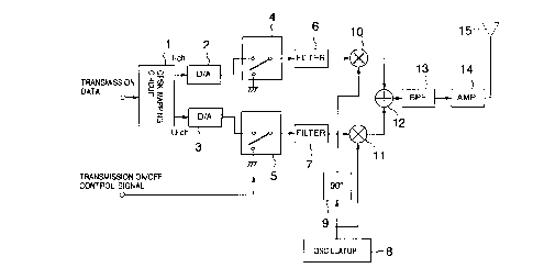
In Fig. 4, numeral 1 denotes a QPSK mapping circuit, 2 and
3 D/A converters, 4 and 5 switches, 6 and 7 band
restriction filters, 8 an oscillator, 9 a 90-degree phase
shifter, 10 and 11 multipliers, 12 an adder, 13 a band pass
filter (BPF), 14 an amplifier and 15 an antenna.
Operation of the first embodiment is now
explained. Transmission data is first inputted to the QPSX
mapping circuit 1 and is mapped in the signal point
arrangement of the QPSK. Actually, signals are arranged as
shown in Fig. 3. Signals for the I channel and Q channel
obtained by the arrangement are converted into analog
signals by the D/A converters 2 and 3. The respective
analog signals converted by the D/A converters are turned
on and off by the switches 4 and 5 in accordance with a
transmission on/off control signal and are band-restricted
by the band restriction filters 6 and 7. The signals from
the filters are subjected to the quadrature modulation by
means of the oscillator 8, the 90-degree phase shifter 9,
the multipliers 10 and 11, the adder 12 and the band pass
filter 13 and the signal subjected to the quadrature
modulation is amplified by the amplifier 14 to be
transmitted from the antenna 15.
Next, the ramp process is now explained. Fig.
5(a) shows a frame format of a transmission signal
including ramp bits composed of ramps 1 and 2 positioned
before and after data. One burst includes the ramp 1 (10
bits), the ramp 2 (10 bits) and the data (200 bits). Fig.
-- 8
5(b) shows a transmission on/off control signal for
controlling the ramp. The switches 4 and 5 are turned on
in the period of the ramp 1 and is turned off in the period
of the ramp 2.
The reason why a frequency component other than
the transmission band is not increased by means of the
above ramp process is now explained with reference to Figs.
6A and 6B. In the modulation system such as the QPSK
modulation, an envelope becomes zero at a moment not only
upon a transient response but also on the way of
transmission. Since the transmission symbol signals are
band-restricted by the band restriction filters 6 and 7 at
the later stage, the band restriction is ensured even in
the pattern in which the envelope is once reduced to zero
so that the transmission symbol transfers by 180 degrees.
Similarly, the band restriction is also ensured even upon
the beginning of transmission where the envelope starts to
be increased from zero and even upon the end of the
transmission where the envelope is reduced to zero. For
example, as shown in Fig. 6A, when transition is made from
(-1, -1) to (+1, +1), the amplitude of the envelope is once
reduced from 21/2 to zero and then returned to 21/2. As
compared with upon the beginning of transmission (Fig. 6B)
where the amplitude of the envelope is increased from zero
to 21/2 in the time period of T (T represents one symbol
period) upon the beginning of transmission, when transition
is made from (-1, -1) to (+1, +1), the amplitude of the
f~
- 9
envelope curve is reduced from 21/2 to zero in the time
period of T/2 and increased from zero to 21/2 in the time
period of T/2. In this manner, variation of the envelope
is larger on the way of transmission than immediately after
the beginning of transmission and accordingly by
suppressing leakage power between adjacent channels during
transmission by using the filters 6 and 7, the practical
ramp process can be performed by on and off control of
transmission by means of the switches 4 and 5.
Fig. 7 shows comparison of a ratio (dBc) of
leakage power to the adjacent channel versus carrier power
in the case of the present invention and the case where the
ramp process with four bits (seven values) or infinite
accuracy is performed in the QPSK modulation system. It is
understood that a difference of leakage power to the
adjacent channel between the case of the present invention
and the case where the ramp process with the infinite
accuracy is performed is as very small as 0.7 dB at the
maximum. In the above comparison, the ramp process has
been performed by approximating the Hunning window for 10
symbols of the ramp. In the case of four bits accuracy,
the Hunning window is approximated by seven values, and in
the case of the infinite accuracy, the Hunning window is
approximated by the infinite accuracy.
As described above, according to the first
embodiment, in the modulation system in which the envelope
of signal is reduced to zero on the way of transmission,
the ramp process can be easily realized by the on and off
4 ~ ~-
control of transmission by the switches and the filtering
process.
In the embodiment, although the QPSK modulation
system is used, the modulation system of 8PSK, 16PSK,
16APSK, 32APSK, 16QAM, 32QAM, 64QAM and 256QAM, in which
only the number of bits in serial-to-parallel conversion
and the mapping method for I and Q channels are different,
can be used to realize the present invention by the same
configuration of the transmission apparatus.
(SECOND EMBODIMENT)
The second embodiment of the present invention is
now described. In the first embodiment, the ramp process
of the transmission apparatus is performed by using the
analog switches, while in the second embodiment the
transmission on/off control signal is supplied to the ramp
circuit to which I and Q channel signals are supplied, to
control digital data so that outputs of D/A converters
connected to a ramp circuit are controlled to be reduced to
zero except the transmission time.
Fig 8 schematically illustrates a transmission
apparatus according to the second embodiment of the present
invention. In Fig. 8, numeral 21 denotes a QPSK mapping
circuit, 22 a ramp circuit, 23 and 24 D/A converters, 25
and 26 band restriction filters, 27 an oscillator, 28 a 90-
degree phase shifter, 29 and 39 multipliers, 31 an adder,
32 a band pass filter (BPF), 33 an amplifier and 34 an
antenna.
Operation of the second embodiment is now
described. Transmission data is first inputted to the QPSK
mapping circuit 21 and is mapped in the signal point
arrangement of the QPSK. Actually, signals are arranged as
shown in Fig. 3. Signals for the I channel and Q channel
obtained by the arrangement are inputted to the ramp
circuit 22 and turned on and off by the transmission on/off
control signal. The on and off controlled signals are
converted into analog signals by the D/A converters 23 and
24 and are band-restricted by the band restriction filters
25 and 26, respectively. The band-restricted signals are
subjected to the quadrature modulation by means of the
oscillator 27, the 90-degree phase shifter 28, the
multipliers 29 and 30, the adder 31 and the band pass
filter 32 and the signals subjected to the quadrature
modulation is amplified by the amplifier 33 to be
transmitted from the antenna 34.
Next, the ramp process is now explained. Fig. 9
schematically illustrates a practical example of the ramp
circuit 22 and the D/A converters 23 and 24. In Fig. 9,
numerals 41 and 42 denote AND circuits, and 43 and 44 2-bit
D/A converters. In the embodiment, since analog values of
+1 and 0 must be outputted, the D/A converters 43 and 44 of
two bits are used. Fig. 10 shows a truth table of the 2-
bit D/A converter.
In Fig. 10, data X of 2-bit data XY represents
the most significant bit (MSB) in Fig. 9 and data Y
~ ~ ~,q fk
- 12 -
represents the least significant bit (LSB) in Fig. 9. The
2-bit D/A converter produces an analog value of 0 for the
value of xY of Noon/ an analog value of +1 for N01N, and
analog value of -1 for "11".
The case where the transmission on/off control
signal is //ON iS now explained. Even when the input data I
or Q is any of NON and Nl N, the ramp circuit supplies N0ON
to the 2-bit D/A converters which in turn output an analog
value of 0. This corresponds to the origin of Fig. 6B.
The case where the transmission on/off control
signal is I~lN is now explained. When the input data I or Q
is NON, the ramp circuit supplies N01N to the 2-bit D/A
converters which in turn output an analog value of +1. On
the other hand, when the input data I or Q is NlN, the ramp
circuit supplies NllN to the 2-bit D/A converters which in
turn output an analog value of -1. That is, when the value
of (I, Q) is (0, 0), the output of the 2-bit D/A converters
43, 44 corresponds to (+1, +1) of Fig. 6B. Similarly, (0,
1) corresponds to (+1, -1), (1, 0) corresponds to (-1, +1)
and (1, 1) corresponds to (-1, -1). In this manner, the 2-
bit D/A converters produce the analog value corresponding
to the value of (I, Q) upon transmission and reduce the
amplitude of the analog value to zero upon stop of
transmission.
As described above, according to the second
embodiment, the transmission on/off control signal is
supplied to the ramp circuit, to which the I and Q channel
signals are supplied, so that the output of the D/A
-
- 13 -
converters are controlled to be reduced to zero except for
the transmission time to thereby realize the ramp process
simply. Further, the ramp circuit can be realized by a
simple configuration of two AND circuits and it is
sufficient for the D/A converter to operate with two-bit
accuracy.
In the embodiment, although the QPSK modulation
system is used, the modulation system of 8PSK, 16PSK,
16APSK, 32APSK, 16QAM, 32QAM, 64QAM and 256QAM, in which
only the number of bits in serial-to-parallel conversion
and the mapping method to I and Q channels are different,
can be used to realize the present invention by the same
configuration of the transmission apparatus.