Language selection

Search

Patent 2201445 Summary

Third-party information liability

Some of the information on this Web page has been provided by external sources. The Government of Canada is not responsible for the accuracy, reliability or currency of the information supplied by external sources. Users wishing to rely upon this information should consult directly with the source of the information. Content provided by external sources is not subject to official languages, privacy and accessibility requirements.

Claims and Abstract availability

Any discrepancies in the text and image of the Claims and Abstract are due to differing posting times. Text of the Claims and Abstract are posted:

  • At the time the application is open to public inspection;
  • At the time of issue of the patent (grant).
(12) Patent: (11) CA 2201445
(54) English Title: HYBRID, SATURABLE REFLECTOR FOR MODE-LOCKING LASERS
(54) French Title: REFLECTEUR SATURABLE HYBRIDE POUR LASERS A SYNCHRONISATION DE MODES
Status: Expired and beyond the Period of Reversal
Bibliographic Data
(51) International Patent Classification (IPC):
  • H01S 3/1112 (2023.01)
(72) Inventors :
  • SULLIVAN, BRIAN THOMAS (Canada)
  • ALCOCK, ALFRED JOHN (Canada)
(73) Owners :
  • NATIONAL RESEARCH COUNCIL OF CANADA
(71) Applicants :
  • NATIONAL RESEARCH COUNCIL OF CANADA (Canada)
(74) Agent: J. WAYNE ANDERSONANDERSON, J. WAYNE
(74) Associate agent:
(45) Issued: 2005-01-11
(22) Filed Date: 1997-04-10
(41) Open to Public Inspection: 1997-10-15
Examination requested: 2001-02-12
Availability of licence: N/A
Dedicated to the Public: N/A
(25) Language of filing: English

Patent Cooperation Treaty (PCT): No

(30) Application Priority Data:
Application No. Country/Territory Date
60/015,424 (United States of America) 1996-04-15

Abstracts

English Abstract


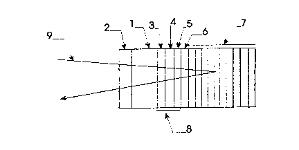
A mode-locking device for a laser operating at a defined wavelength, has a
substrate, transparent to the defined wavelength, with a front side for
receiving
incident radiation and a back side. An anti-reflection coating is formed on
the front
side to minimize reflection loss at the defined wavelength. A quantum well
structure
is arranged on the back side. A high reflectance structure is arranged behind
the
quantum well structure in such a way that an electric field peak in the
incident
radiation substantially coincides with said quantum well structure. This
device offers
a more reliable and less costly approach for the production of non-linear
mirrors since
the layers of the dielectric stack do not have to be formed by epitaxial
deposition.


Claims

Note: Claims are shown in the official language in which they were submitted.


We Claim:
1. A mode-locking device for a laser operating at a defined wavelength,
comprising:
a) a substrate, transparent to the defined wavelength, with a front side for
receiving incident radiation and a back side;
b) an anti-reflection coating is formed on the front side to minimize
reflection
loss at the defined wavelength;
c) a quantum well structure is arranged on the back side; and
d) a high reflectance structure is arranged behind the quantum well structure
in such a way that an electric field peak in said incident radiation occurs at
said quantum well structure.
2. A mode-locking device as claimed in claim 1, where said quantum well
structure is deposited epitaxially on said back side of said substrate.
3. A mode-locking device as claimed in claim 2, wherein said quantum well
structure comprises a quantum well layer sandwiched between two outer
layers, the thickness and materials of said layers being selected such that
said
quantum well will absorb some light at said defined wavelength.
4. A mode-locking device as claimed in claim 3, wherein said high reflectance
structure comprises a stack of layers, at least one of which is a non-
epitaxial
layer.
5. A mode-locking device as claimed in claim 4, wherein all of said layers
forming said stack of layers are non-epitaxial layers.
6. A mode-locking device as claimed in claim 4, wherein said layers forming
said stack of layers are Nb2O5/SiO2 layers.
7. A mode-locking device as claimed in claim 3, wherein said substrate is made
of indium phosphide (InP).
8. A mode-locking device as claimed in claim 3, wherein said quantum well
structure comprises a GaInAs layer sandwiched between a pair of AlInAs
layers.
9. A mode-locking device as claimed in claim 8, wherein said AlInAs layers
have a thickness .lambda./4, where .lambda. is said predefined wavelength.


10. A mode-locking device as claimed in claim 8, wherein said wavelength is
about 1.5µm.
11. A method of fabricating a mode-locking device for a laser operating at a
defined wavelength, comprising the steps of:
a) providing a substrate, transparent to said defined wavelength, having a
front side for receiving incident radiation and a back side;
b) providing an anti-reflection coating on said front side to minimize
reflection loss at said defined wavelength;
c) providing a quantum well structure on said back side; and
d) providing a high reflectance structure behind said quantum well structure
in such a way that an electric field peak in said incident radiation occurs at
said quantum well structure.
12. A method as claimed in claim 12, wherein said quantum well structure is
deposited epitaxially on said back side of said substrate.
13. A method as claimed in claim 12, wherein said quantum well structure is
formed by sequentially depositing epitaxially a first outer layer on the back
side of said substrate, depositing epitaxially a quantum well layer on said
first
layer, and depositing epitaxially a second outer layer on said quantum well
layer, the thickness and materials of said layers being selected such that
said
quantum well will absorb some light at said defined wavelength.
14. A method as claimed in claim 13, wherein said high reflectance structure
is
formed by depositing a stack of layers, at least one of which is deposited by
non-epitaxially, on said second outer layer of said quantum well structure.
15. A method as claimed in claim 14, wherein all of said layers forming said
stack
of layers are formed non-epitaxially.
16. A method as claimed in claim 15, wherein said layers forming said stack of
layers are formed by a method selected from the group consisting of
evaporation, ion plating, and sputtering.
17. A method as claimed in claim 11, wherein said substrate is mad eof indium
phosphide (InP).
18. A method as claimed in claim 13, wherein said quantum well structure
comprises a GaInAs layer sandwiched between a pair of AlInAs layers.

19. A method as claimed in claim 18, wherein said AlInAs layers have a
thickness
.lambda./4, where .lambda. is said predefined wavelength.
20. A method as claimed in claim 11, wherein said wavelength is about
1.5µm.

Description

Note: Descriptions are shown in the official language in which they were submitted.


CA 02201445 2004-04-22
hybrid, Saturdblc Reflector For Mode-Locking Lasers
'this invention relates generally to lasers, and in particular to~a modo-
locking
device for low gain lasers.
hers employ a resonant cavity to generate resonant light. It is known that a
laser can operate in a number of different frequency modes due to the
existence of off
i axis resonances in the laser cavity. Sucte off axis mocks are generally
undesirable
because they lead to dispersion lasses i>i transmission. There is a need in
the art to
lock lasers into a~single mode of operation,
For approximately ten years a number of researchers have been investigating
the ttse of quantum well (QW) or multiple quantum well structure (MQWSs) as
to satursble absorbers for mode-locking low gain lasers. 'fhe interest in this
approach
lies in the potential for eng~noaring the chataaeristics of such an absorber
and
optitttizing ii for a particular laser wavelength. Both inttacavity elements
and -
nvplinearreflectors have bear studied.
More re!ccatly a satutablc Bragg reflector incorporating a single quantum well
t 5 to prvovide a small amount (e.g. 1 - 29~e) ofsaturable lass has bten
proposed. Tsuda et
al. ppt. Lett. Z0, 1406 (1995) describe such a device, based on AIAsIAIGaAs,
which .
they have used successfully to modsrlock both T i:Sapphire and Cr,LiSAI~
lasers
operating near 850 nm. The $ragg reflector ihustrated in their paper, was
grown by
rxAOlecular beam epilaxy (MBE) and consisted of 30 high/low index pairs with a
single
zo GaAs quantum well buried in one of the layers. The entire structure, which
was grown
epitaxixtly on a GaAs substrate, acted as a high reflectivity mirror having an
intensity
dependant reflectivity governed by the saturable absorption behaviour of the
quantmn
well. An important feature of this scheme is the fact that the effective
saturaiion
intensity can be controlled by varying the location of the quantum well within
the
25 mulri-layer reflector siructure. The Quantum Well was located at ar<
electric field
maximum in the first Iayer of the Bragg reflector.
A drawback of xhis saturable reflector, however, is the fact that the high
reflectance stack has to lie deposited cpitaxially in order to deposii the
epitaxial
Quantum Well structure. Hence great care has to ire taken in the fabrication
of sraeh a
-1-

CA 02201445 2003-11-20
mirror to ensure that non saturable losses, particularly scattering, are
extremely
small, especially as a large number of layers, typically around 60, have to be
grown
to achieve the desired reflectance (typically around 99%). The fabrication of
low
reflectors by molecular beam epitaxy (MBE) is thus very difficult.
Furthermore, the
MBE deposition rate is slow compared to other processes.
A hybrid reflector, incorporating both epitaxially deposited semiconductor
layers and evaporated dielectric layers, has been developed by U. Keller, et
al Opt.
Lett. 17,505 (1992). It is not capable of operating as a saturable Bragg
reflector.
An object to the invention is to alleviate this problem.
Summary of the Invention
According to the present invention there is provided a mode-locking device for
a laser
operating at a defined wavelength, comprising a substrate, transparent to said
defined
wavelength, having a front side for receiving incident radiation and a back
side; an
anti-reflection coating on said front side to minimize reflection Loss at said
defined
wavelength; a quantum well structure arranged on said back side; and a high
reflectance structure arranged behind said quantum well structure in such a
way that
an electric field peak in said incident radiation substantially coincides with
that of said
quantum well structure.
Ideally the electric field peak should coincide with the quantum well
structure,
although some departure from coincidence can be tolerated. The greater the
departure
from coincidence, the less the difference in the reflectance between the
saturated and
unsaturated cases. The acceptable level is a matter of choice that can readily
be
determined by a person skilled in the art depending on the particular
application.
The quantum well structure normally consist of three epitaxial layers, a
quantum well layer and two outer layers. With this arrangement the high
reflectance
structure can be formed of a stack of layers deposited by non-epitaxial means,
such as
evaporation, ion plating, sputtering etc., resulting in a simpler, more
reliable structure.
The device in accordance with the invention can be operated as a saturable
Bragg reflector where in the high reflectance structure can be a stack
deposited non-
-2-

2201445
epitaxially while quantum well structure is deposited epitaxially. The light
must now
be incident on the quantum well structure from the substrate side.
An important advantage of the invention is the possibility of greatly reducing
the number of required epitaxially grown layers and achieving a high
reflectivity by
means of the non-epitaxially deposited layers.
The mode-locking device can be used as a mode-locker for low gain laser
media such as Ti:Sapphire, Cr:LiSAF and CR:YAG. Passive mode lockers greatly
simplify the gain of the laser.
The invention also provides a method of fabricating a mode-locking device for
1o a laser operating at a defined wavelength, comprising the steps of
providing a
substrate, transparent to said defined wavelength, having a front side for
receiving
incident radiation and a back side; providing an anti-reflection coating on
said front
side to minimize reflection loss at said defined wavelength; providing a
quantum well
structure on said back side; and providing a high reflectance structure behind
said
15 quantum well structure in such a way that an electric field peak in said
incident
radiation substantially coincides with that of said quantum well structure.
The invention will now be described in more detail, by way of example only,
with reference to the accompanying drawings, in which:-
Figure 1 is a schematic diagram of a mode locking device in accordance with
20 the invention;
Figure 2 is a plot of a simulation showing the electric field peaking at the
quantum well layer;
Figure3 is a plot showing the difference in reflectance for the saturated and
unsaturated cases for Figure 1;
25 Figure 4 is a plot of a simulation showing the electric field at a minimum
at
the quantum well layer;
Figure 5 is a plot showing the difference in reflectance for the saturated and
unsaturated cases for Figure 4.
-3-

CA 02201445 2003-11-20
Referring now to Figure l, the mode-locking device comprises a 0.5 mm
transparent InP substrate I having a refractive index n of 3.17. On the front
side of the
substrate 1 is deposited, for example, by ion plating techniques an anti-
reflective layer
2 consisting of NbZ05 with a refractive index n of 2.31 and SiOz with a
refractive
index n of 1.48.
On the back side of the transparent substrate is deposited by molecular beam
epitaxy a quantum well structure 8 consisting of a first AIInAs layer 3 having
an
optical thickness of 7l/4, where ~, is the wavelength of the radiation, for
example, 1.5
Eun, and a refixetive index n of 3.21.
Next an 8nm GaInAs quantum well layer 4 with a refractive index n of 3.51 is
grown by molecular beam epitaxy on the first layer 3 molecular beam epitaxy.
Subsequently a second AIInAs layer 5 having an optical thickness of 7U4, and a
refractive index n of 3.21 is grown epitaxially onto the quantum well layer 4.
Finally
an additional 2 nm GaInAs layer 6 is grown epitaxially onto the second outer
layer S.
~e layer 6 has a refractive index n of 3.51 and serves as a protective or
capping layer
for the AIInAs layer S.
Finally a stack of dielectric NbZ05 /SiOi layers 7 is deposited by ion plating
onto the outermost epitaxial layer 6. The NbZ05 layers have a refractive index
n of
2.31 and SiOz have a refractive index n of 1.48. The layers Gave an optical
thickness
of 7v.°I4. The optical thickness is the physical thickness multiplied
by the refractive
index. Typically there are 10 or 11 layers of aliemately high and low
refractive index.
The stack typically has a reflectance of around 98%.
The thickness and materials of the layers are chosen such that when the laser
light is incident on the antireflective layer 2, the location of one of the
electric field
pas, within the complete structure, substantially coincides with that of the
quantum
well.
The described mode-locking device provides a laser reflector that has a low
intensity reflectivity, R,,, and a high intensity reflectivity Rf,, such that
R~ is less than
-4-

CA 02201445 2003-11-20
RH but is still sufficiently high to permit laser oscillation to build up in a
suitably
designed laser system.
Although it is possible to fabricate such reflectors at many different
wavelengths, the 1.5 pm region is particularly interesting since this is an
important
wavelength region for optical communications. Both erbium fiber and Cr4+--
doped
lasers operate in this region. In addition, InP can be used as the transparent
substrate
for an InAIAs/InGaAs quantum well structure.
Using the optical constants for these materials, a suitable structure, which
places an electric field peak in the quantum well, has been designed and
modeled
numerically while tests carried out with an ion-plating facility have
demonstrated that
high quality Nb205/Si02 layers, capable of providing high reflectivity at 1.5
pm, can
be deposited on top of the MBE-grown semiconductor layers.
In use the device provides a passive mode-locker for a low gain laser, such as
Ti:Sapphire and Cr:LiSAF. Incident light 9 enters through the anti-reflective
coating
on the front side, passes through the quantum well structure and is reflected
in the
dielectric stack 7.
To show the importance of having an electric field maximum at the position of
the QW, numerical modeling was used to examine two different cases.
First, a high reflector was designed such that the electric field peaked at
the
quantum well layer 4 (Figure 2). Then to simulate the unsaturated case, an
extinction
coefficient was added to the Quantum well material, while for the saturated
case the
extinction coefficient was zero. The difference in reflectance for the
saturated and
unsaturated cases is shown in Figure 3. This shows that a change in
reflectance, AR,
between the saturated and unsaturated case of approximately 2.4% would be
observed.
Next, a high reflector was designed such that the electric field is a minimum
at
the Quantum well layer 4 (Figure 4). The difference in reflectances for the
saturated
and unsaturated cases is shown in Figure 5. Here it is apparent that there is
no
significant change in reflectance, and hence the device is less likely to be
effective as
a saturable reflector. This modeling shows that it is important to design the
high
-5-

2201445
reflectance structure properly in order for the hybrid saturable reflector to
achieve the
maximum change in reflectance.
The described structure provides a passive mode-locking device that can be
fabricated with two or three MBE layers and a dielectric stack using
significantly
fewer layers than the prior art.
-6-

Representative Drawing
A single figure which represents the drawing illustrating the invention.
Administrative Status

2024-08-01:As part of the Next Generation Patents (NGP) transition, the Canadian Patents Database (CPD) now contains a more detailed Event History, which replicates the Event Log of our new back-office solution.

Please note that "Inactive:" events refers to events no longer in use in our new back-office solution.

For a clearer understanding of the status of the application/patent presented on this page, the site Disclaimer , as well as the definitions for Patent , Event History , Maintenance Fee  and Payment History  should be consulted.

Event History

Description Date
Inactive: First IPC assigned 2024-01-24
Inactive: IPC assigned 2024-01-24
Inactive: IPC expired 2023-01-01
Inactive: IPC removed 2022-12-31
Time Limit for Reversal Expired 2008-04-10
Letter Sent 2007-04-10
Grant by Issuance 2005-01-11
Inactive: Cover page published 2005-01-10
Pre-grant 2004-10-18
Inactive: Final fee received 2004-10-18
Revocation of Agent Request 2004-09-03
Appointment of Agent Request 2004-09-03
Notice of Allowance is Issued 2004-05-05
Letter Sent 2004-05-05
Notice of Allowance is Issued 2004-05-05
Inactive: Adhoc Request Documented 2004-05-04
Inactive: Received pages at allowance 2004-04-22
Amendment Received - Voluntary Amendment 2004-04-22
Inactive: Office letter 2004-02-04
Inactive: Approved for allowance (AFA) 2004-01-26
Inactive: Adhoc Request Documented 2004-01-23
Inactive: Delete abandonment 2004-01-23
Inactive: Abandoned - No reply to Office letter 2003-12-08
Amendment Received - Voluntary Amendment 2003-11-20
Inactive: Office letter 2003-09-08
Amendment Received - Voluntary Amendment 2003-08-22
Letter Sent 2003-05-08
Reinstatement Requirements Deemed Compliant for All Abandonment Reasons 2003-04-16
Deemed Abandoned - Failure to Respond to Maintenance Fee Notice 2003-04-10
Inactive: S.30(2) Rules - Examiner requisition 2003-02-24
Appointment of Agent Requirements Determined Compliant 2002-02-22
Inactive: Office letter 2002-02-22
Revocation of Agent Requirements Determined Compliant 2002-02-22
Revocation of Agent Request 2002-02-04
Appointment of Agent Request 2002-02-04
Amendment Received - Voluntary Amendment 2001-03-06
Letter Sent 2001-02-22
All Requirements for Examination Determined Compliant 2001-02-12
Request for Examination Requirements Determined Compliant 2001-02-12
Request for Examination Received 2001-02-12
Inactive: Inventor deleted 2000-07-06
Application Published (Open to Public Inspection) 1997-10-15
Inactive: IPC assigned 1997-07-07
Inactive: First IPC assigned 1997-07-07
Inactive: Filing certificate - No RFE (English) 1997-06-23
Inactive: Applicant deleted 1997-06-20
Filing Requirements Determined Compliant 1997-06-20
Letter Sent 1997-06-20
Inactive: Filing certificate - No RFE (English) 1997-06-20
Inactive: Applicant deleted 1997-06-20
Inactive: Inventor deleted 1997-06-16

Abandonment History

Abandonment Date Reason Reinstatement Date
2003-04-10

Maintenance Fee

The last payment was received on 2004-03-22

Note : If the full payment has not been received on or before the date indicated, a further fee may be required which may be one of the following

  • the reinstatement fee;
  • the late payment fee; or
  • additional fee to reverse deemed expiry.

Please refer to the CIPO Patent Fees web page to see all current fee amounts.

Fee History

Fee Type Anniversary Year Due Date Paid Date
Application fee - standard 1997-04-10
MF (application, 2nd anniv.) - standard 02 1999-04-12 1999-03-10
MF (application, 3rd anniv.) - standard 03 2000-04-10 2000-02-21
Request for examination - standard 2001-02-12
MF (application, 4th anniv.) - standard 04 2001-04-10 2001-02-13
MF (application, 5th anniv.) - standard 05 2002-04-10 2002-02-26
Reinstatement 2003-04-16
MF (application, 6th anniv.) - standard 06 2003-04-10 2003-04-16
MF (application, 7th anniv.) - standard 07 2004-04-13 2004-03-22
Final fee - standard 2004-10-18
MF (patent, 8th anniv.) - standard 2005-04-11 2005-04-08
MF (patent, 9th anniv.) - standard 2006-04-10 2006-04-07
Owners on Record

Note: Records showing the ownership history in alphabetical order.

Current Owners on Record
NATIONAL RESEARCH COUNCIL OF CANADA
Past Owners on Record
ALFRED JOHN ALCOCK
BRIAN THOMAS SULLIVAN
Past Owners that do not appear in the "Owners on Record" listing will appear in other documentation within the application.
Documents

To view selected files, please enter reCAPTCHA code :


To view images, click a link in the Document Description column. To download the documents, select one or more checkboxes in the first column and then click the "Download Selected in PDF format (Zip Archive)" or the "Download Selected as Single PDF" button.

List of published and non-published patent-specific documents on the CPD .

If you have any difficulty accessing content, you can call the Client Service Centre at 1-866-997-1936 or send them an e-mail at CIPO Client Service Centre.


Document
Description 
Date
(yyyy-mm-dd) 
Number of pages   Size of Image (KB) 
Representative drawing 1997-11-19 1 5
Abstract 2003-11-20 1 19
Description 2003-11-20 6 253
Claims 2003-11-20 3 96
Cover Page 1997-11-19 1 49
Abstract 1997-04-10 1 21
Description 1997-04-10 6 262
Drawings 1997-04-10 5 105
Claims 1997-04-10 3 107
Description 2004-04-22 6 238
Cover Page 2004-12-08 1 36
Courtesy - Certificate of registration (related document(s)) 1997-06-20 1 129
Filing Certificate (English) 1997-06-23 1 165
Reminder of maintenance fee due 1998-12-14 1 110
Acknowledgement of Request for Examination 2001-02-22 1 179
Courtesy - Abandonment Letter (Maintenance Fee) 2003-05-08 1 176
Notice of Reinstatement 2003-05-08 1 167
Commissioner's Notice - Application Found Allowable 2004-05-05 1 161
Maintenance Fee Notice 2007-05-22 1 173
Correspondence 2002-02-04 1 33
Correspondence 2002-02-22 1 13
Correspondence 2002-02-22 1 17
Fees 2003-04-16 1 28
Fees 2002-02-26 1 32
Fees 2004-03-22 1 27
Correspondence 2004-04-22 4 98
Correspondence 2004-09-03 2 60
Correspondence 2004-10-18 2 65
Fees 2005-04-08 1 24
Fees 2006-04-07 1 25