Note: Descriptions are shown in the official language in which they were submitted.
CA 02202863 1997-04-16
WO96~12230 . ~Cl.__ C/ lLlS
P14913PC
Title:
SYSTEM AND METHOD FOR PROCESSING OF MEMORY DATA AND
COMMUNICATION SYSTEM COMPRISING SUCH SYSTEM.
Tr~rT~NTr~r~ FIELD
The present invention relates to a system and a method
respectively for pror~cc; n~ of memory data The invention
also relates to a ~ ; r~tions system comprising such a
system for pror~ec;n~ of memory data.
Memory ~ ;r~tion for stored data variables within a data
pror~Ce;n~ system often C~ ^ a great part of the capacity
that is available within the data ~ i r~tion unit for
i~lL~, iriqtion between the location for storing the
variables and the unit for data prrr~cc; n5
It is common that a number of variables share the memory area
of a word. Variables sharing the memory area of a word is
~ff;r;~nt from a memory packing point of view. Among others
such sharing may contribute in reducing the number of memory
accesses. In spite thereof, however, the available capacity
is sometimes not used in an ~ffiri~nt way.
For exampie in large systems ~ c~sing data in real time
which require very much memory it is particularly i",~
to have an organisation of the memory so that a high storing
and, ~ r~tion capacity can be provided.
STATE OF ART
Many different alternatives have been suggested for how to,
in an ~ffir;~nt way, use the capacity for storing and
~- ; c~tion between the location for storing of variables
and that or those units which are to process data. Tt is a
problem that the memories are comparatively slow as compared
CONFIR~IAT~ON
COPY
CA 02202863 1997-04-16
WO 96/12230 . P~ a/01~l5
to the data processing units from an internal point of view.
~ith the known solutions to these problems it has been
intended to achieve an ef f icient usage of memory A~
S In US-A-4 354 231 cache-t~ hn; ~ is used . The cache-
technique is based on storing memory data that is often
addressed in a fast memory, a so called cachc y which is
controlled by various algorithms. lutL~LoL memory operations
directed towards a slow memory are often handled by the
cachc - - y which has an access time which is r-.nncitl~ hly
shorter. According to US-A-4 354 231 an address calculation
is initiated in good time before the relevant program
instructions are to be executed in order to reduce the
waiting time The ~ y ~ according to the above
mentioned US-,~ t for reducing the time for in:,Llu~,~ion
execution comprises a buffer memory in which instructions
read from the program memory are ~seguentially and t~.~ CLily
stored in an execution buffer. The execution buffer is
provided with in~L~u~;~1ons of ~i;f~l~pnt kinds, of which a
first kind relates to writing or reading in the data memory
and a second kind of instructions places address PCL . L~L a
in a register memory. First and second activation means
which are intended for initiation- -L~-sL~l of address
PCL LIC:L~: from the register memory to the address pro~
means for modifying the address when an indication is present
in a registering means and the instruction is in turn to be
handled and is of the above mentioned first kind, or for
removing the indication from the registration means after the
trAn~-~i Cci nn has been effected and the second activation
means which are connected to the address hAn~ll in~ means,
respectively respond to a base address read out from a
reference memory to the address hAn~ll in~ means for initiation
- of a calculation of the absolute address when at the same
time none of the ahead stored instructions are of the second
kind, i.e. the kind which places the address PCIL ~ Lt~ , in
the register memory etc. Thus a certain time saving is
.
CA 02202863 1997-04-16
WO96/12230 . J
3
provided thereby through an efficient usage of the time.
~owever, except for the time savirigs, which even may be
minor, memory data of a system can be 1O~~A1;7~ in such a way
that the application of the cache-tD~hn~ ~ indeed does not
give the desired result and may in fact be in~ff;~i~nt~
Furthl t:, the cache-technique is not efficient for
randomly occurring data Al"~ qR~3R,
EP-A-O 439 025 rli $~-1 oc ~c a data processor having a deferred
cache load which comprises an instruction prefetch unit, a
memory, a ~L.J~ Ul bus and a function unit wherein the
latter Collv~dL~,~ logical addresses and provides for storing of
preceding memory At~ RS~C in a cache memory and for storing
of i - = n~ memory requests. FUL ~' ~ a comparison of
addresses is done and if there is corr~sp~n~ n~, memory data
of a preceding request is reused.
~lowever, the system according to EP-A-O 439 025 ~L.~ C.-C
pre-buffering or prefetching which sometimes is inconvenient.
Fur~h~ ~:, it is a precondition that data arrive is
regularly, i e. that data are not spread out. Furth~ e an
int ~ii Ate buffer is required. Consequently the system is
~_ liçAted and it cannot be used for randomly occurring data
etc. which both are serious drawbacks.
Other known ways through which it is an intended to obtain an
efficient usage of Arc~ccF~c and to provide a high capacity
are based on an interleaving organization. The memory is
organized in a number of memory banks and in practice it
behaves like a fast memory. On condition that consecutive
memory A~-c~cc~c are directed towards different memory banks,
interleaving technique may ~ in some cases provide
comparatively good results.
~ -
However, in many cases it is desirable to fuFther reduce the
_
CA 02202863 1997-04-16
wo 96~12230 1 ~ ul~15
memory ~ r~Cs~q. Furth~ t the interleaving technique is
l~ff;~ 3nt only on condition that consecutive memory ~r~cs~c
are not directed towards the same memory bank. For
consecutive memory ~nc~ccl~c addressing one and the same
memory word, the ~ffir;c~n~y can not be improved by known
methods .
SUMMARY OF THE TNVENTION
It is an object of the present invention to provide a system
and a method respectively for pro~Pcg;n~ of memory data
wherein the data ~~ ;n~ capacity is used as efficiently
as pocg;hl~ art;~ A~ly it is an object of the invention to
provide a system having such a memory organization that
F~ff;r~; ~nt storing as well as ~ff;~ nt ;c~tion between
storing location and data proc~CC; n~ units can be provided
It is particularly an object of the invention to provide a
system and method wherein memory ~nr~PqRI~c can be used as
efficiently as poc5;hle. Fu~ it is an ob~ect of the
invention to provide a system and a method respectively
wherein the number of memory ~ CC~5 can be reduced
Fu ~ ~' ~ it is a particular obj ect of the invention to
provide a system apd a method that reduces the number of
::.nr~cc~C in connection with prnl-~cg;n~ of indexed variables
and/or partial variables and sub-data variables.
A particular ob~ect of the invention is to provide a system
and a method respectively through which a -nnc; ~ rable
increase in capacity can be provided, particularly
; n~ ~p~n~l~ntly of which memory organization that is used. More
particularly it is an object o the invention to provide a
system which uses interleaving and more particularly data
(pre)buffering which from a capacity point of view is highly
ef f icient
A further object of the invention is to provide a system in
which index add~essed variables of varying format size and in
CA 02202863 1997-04-16
wo96/12230 : PCTISE95/01215
which the number of memory z~ ee~e is reduced in relation to
the actual number of memory I~-r~cqPc,
FUL i ' e it is a particular object of the invention to
provide a system and a method respectively with a number
parallel Leyue,Ling sources in which an ~ff~ nt usage of
memory ~ qs~q is provided.
Still a further object of the invention is to provide a
~ ;r~qtions system ~- c;n~ a system for ~,, o~ ~c~;n~ of
memory data as referred to above which efficiently uses the
capacity and which in an optimal way uses memory Ar ~ ~qq ~q .
A particular object is to provide a system (and a method)
which can be used when variables are spread across the
memory, data may arrive randomly. Most particularly to
provide such a system when a normal cache cannot be used
because of said irregularities.
Moreover it is a particular object to provide a system which
can be used and which is ~f~ nt when the variables are not
regularly returnea to and when variables are located over an
address area which substantially is not limited.
~hese as well as other ob; ects are achieved through a system
and a method respectively in which directly or indirectly
consecutive requests towards the same physical word address
for variables, the memory is only activated for the first
memory access on the actual word address, the memory data or
read data of which thus is multiple-used. Thus the ob~ects
are achieved through memory accesses having the same word
address as a preceding - particularly the preceding - access,
use memory data, part; ~ ~ly read data, on the previous
access. Thus a memory access is saved. According to
advantageous: ' ~ '; the variables are indexed VA~;:~hl ~e,
partial variables or sub-variables.
.
CA 02202863 1997-04-16
wo 96/-2230 ~ ~ PCT/SE9s/01215
According to a particularly advantageous: 'i t the
memory system uses an interleavlng technique and particularly
advantageously with data (pre)buffering or prefetching.
Particularly buf ~ering in this case means that address
calculations and memory requests for reading of variables .
from the memory take place in advance and are L~ cu.sreLle:d to
the data pro~cci n~ unit before data is reguired by its
program steps . This provides a l~nc; ~able increase in
capacity. Particularly data is sent directly to the operating
register without requiring any il3~ te buffer.
According to an advantageous ~mhQ~l; t of the invention,
; n~1~r~n~1~ntly of which variable that is intended in the read
out memory word, an address i,3r~,L".. I ion part is obtained at
every request when a physical memory address relating to a
logical address is represented to the variable in a known
way.
According to a particular ' ~ the invention intends to
provide a reduction of ,v~se-_u -ive read ~ cs~c directed
towards the same word address in the memory.
More particularly, accoraing to an a~vc~l~c~ ua F.mhr~i 1,,
consecutive write ~r~qC~,c to variables with the same
25physical word address are reduced. - -
According to an advantageous ~hn~l; 1., for consecutive
write requests of variables having the same physical word
address, the read data of a iirst access is handled
essentially in the same way as in a conventional read access
corr~cr~n~;n~ to the memory access of the write operation for
read-out whereas the second memory access of the write
operation which comprises writing in the memory, is such
that a consecutive write request receives the write data of
the preceding access as its own read data. According to-one
embodiment memory activities for writing are executed for
.
- CA 02202863 1997-04-16
.. WO96/12~30 . r~ SlUl)l~;
- 7
each variable According to an alternate G ' '; L memory
activities for writing are executed when a com=plete variable
word has been processed. Then it is an a~vcl-lL~ye: if the
actual memory address is protected against i~lL~L~Lt:llCe until
all variables of the word are l.L-.ce~ised and the result has
been executed in the memory.
According to an advantageous Pmho(li L index addressed
variables of varying format are used in the data prof~ecci n~
system. In a particular ' - 'i L there are a number of
parallel request sources. The system can thus be used in
parallel for more than one data procPqcin~ unit. This can be
said to give rise to gain in capacity in an indirect way
since the various parallel L~yue:, Ling sources or the data
pr~ sc; n~ units are exposed to fewer access obstacles when
the common memory is requested.
In addition to other advallL.~Gs as referred to in
advantageous ~ a etc. it is an advantage of the
invention that it is not nP~ y to update several means.
BRIEF DESCRIPTION OF THE DRAWINGS
~he invention will in the following be further described in
a non-limiting way under reference to the ;~c _-nying
drawings in which: ~
FIG 1 illustrates an example of a system according to the
invention .
DETAILED DESCRI~TION OF T~E INVENTION
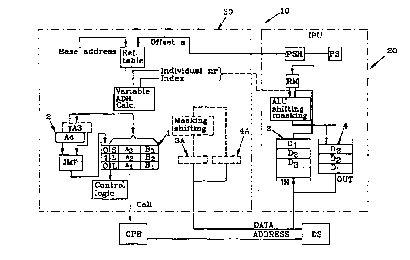
Fig. 1 illustrates a data pro--Pcc; n~ system 10 which
comprises at least one data pr u-~qci n~ unit IPU 20 . In the
shown PmhcJ~ ~ L there is only one data processing unit but
there could as well be two or more. The data processing unit
IPU comprises internal process registers and arithmetical and
logical units ALU intend~d for data prO-~Pcc1ng. mLhe data
CA 02202863 1997-04-16
Wo 96112230 PCT/SEss/0121s
prr~ ce;n~ unit IPU further comprises a program memory
handler PS~, a program memory PS and a register memory RM.
The data pro~eei n~ system lO q~e a common data memory
DS. An asynchronous ~ y~:LdLiOn hetween the data pr~ s~;
unit IPU and the memory DS is according to an ~-lvc-l- L~ Jus
controlled by a ~yl,_l Lv..ization bit. The common
data memory DS for stored V::~Ti :~hl ~e is acoording to an
advantageous ~mhr~Ai- L formed by memory banks through the
use of the so called interleaving tP~hni q--~ . A centrally
controlled bus and access handler (central processor bus~ CPB
carries out the memory request. The central processor bus
CPB controls and keeps information about which memory banks
of the data memory DS which are free and o--c--ri l,A
respectively. Furth-~ ~ the central ~LU~ CIL bus is aware
of the sequential order at activation of various memory
operations. The data pro~ e~in~ system further comprises a
function unit 30 for autonomous h~nAl;n~ of variables. In the
function unit 30 are reference tables and address calculation
circuits for ~ v~ ~iOn of logical addresses to physical
addresses. FUL i ' ~ ~: the function unit 30 comprises logical
circuits, buf f er registers etc . A buf f er register l is
arranged for the physical memory addresses which are
calculated with the assistance of reference tables and
address calculation circuits. For each requested variable
information about memory word address Bi,B2,B3, variable
address A1,A2,A3 as well as the format within the memory word
is stored. Furth, c: information is stored about the
operation type of the requested variable, i . e. normally read
or write type, according S, L, L wherein S denotes writing and
L reading. FurthP ~ a state bit is stored in the buffer
register l. According to an advantageous ~ hsAi t the
buffer memory l , , e~e a so called FIFO-memory ( first
in/first out). The last calculated address is then stored in
an i.~ te buffer 2 as A4. Through comparison means
35 - comprising a comparison circuit JMF, the new, i . e; the last
cal~ulated addFe6s A4 in tùe i.~L '; ~te buffer is compared
CA 02202863 1997-04-16
wo 96112230 , PCT/SE95/0121
to the preceding address A3 in the buf fer register l . If the
addresses are the same ( A3 = A4 ), the mark bit which may be
0 or l, is set.
S The system lO further advd~ J~-ol~ql y ~ c a second
buffer register 3 which also may be of FIFO-type. This serves
as a register for the variables which have been read out and
which may take the function of an operand register for the
data y~ in~ unit TPU. For an extended parallel operation
the system may advant~ ollcly comprise a second inl,, ~ te
register 3A for preparing variables for example relating to
the shifting and masking of the variable within the read
memory word.
A third buffer register 4 may further be dLLdi1yed which also
may be of FIF0-type register for variables which are to be
stored in the data memory DS. According to a particular
may a furthermore a third i~ te register 4A
be dL~ d11yed which among others can be used for further
increasing the l~ffin,~l~nny for c~rtain operations etc.
According to an advc.~dyeous ' ~li 1, t,he ,system operates
as follows. The program store handler PSE~ in the data
processing unit IPU activates, advantageously in advance with
(pre)buffering, a variable request per program step through
giving its logical aadress . This is given through of f set a,
individual number and index and LUL i ' t: the kind of
operation, particularly read or write ( L or S ) . Then the
address calculation is activated via control logic. This
converts the logical address of- the Yariable to the
corresponding physical address with use of a LefeLellce table
which contains information needed for 'providing the
v~L~ion. Before a variable address calculated in this way
is placed in the buffer register l for prn~~~ccin~ the memory
word address part is compared to the memory address of the
preceding variable in the buffer ~egister l. Th:s comparison
CA 02202863 1997-04-16 ~
W0 96/1223~ 1215
is done in the , cnn ~LLally L 3MF which comprises
comparison circuits. If the last calculated variable address
A4 i5 equal to the preceding variable address A3 of the
buffer register, a mark bit i8 set which indicates that the
new data variable .li crns-~C the same memory word as the
preceding variable. When a ~urL~L~cd request towards a memorv
is processed via the central ~L'J~551.JL bus the flag bit
reroutes the request. This results in a memory access or, if
two consecutive memory addresses are the same, it results in
reuse of the read data for the preceding memory access. When
the read data of the preceding memory access is reused, the
read data is already present in the indata buffer of the data
prnn~c5; n~ unit IPU. If there is an ill~ te register 3A
in the function unit 30, data is ~Lc~ LeLlt:d from this
i,. 'i :~te register to the indata buffer 3 of the data
pro~ s~:; n~ unit IPU.
In the following a case relating to consecutive write
L~ Ue~S will be briefly ~licc~lsc~- A write operation as such
comprises two memory ~r-r.l~Cc~c, one for reaa out and one for
write in. In the case of consecutive write requests to data
variables having the same physical word address, reading
means that the read data of the first request is handled in
a way which ~;ulL~::,~ul-ds to that of the read request whereas
the following write request receives data rom the preceding
access as its own read data. This means that the write data
of the preceding variable which is in the data buffer in IPU,
is ~lcll~L~ d to the indata buffer 3 of the data processing
unit IPU. If i~ te registers 3A;4A are used, data is
according to one embodiment transferred from the illL ~ te
register to the indata buffer 3 of the unit IPU for
proc~cc;n~. Consequently the mark bit in combination with the
actual type of operation, i.e. reading or writing, control
the memory activation as well as internal data ~lcll,LeLs
between buffers as well as within the buffer register l. The
parts of the buffer register l which are required for
~ =
CA 02202863 1997-04-16
Wo 96112230 = ~ 5/01215
.
11
variable h:~n~ll in~ are transferred to the buffer of the data
processing unit IPU.
The invention shall of course not be limited to the
~ t:, shown herein but, as mentioned above, a plurality
of data proc~csi n~ units may work in parallel as well as
there are a number of other alternatives. FUL ' e the
variable requests do not have to be directly consecutive but
according to an alternative there may be one or more variable
requests in between in a predet~7~ni n~d manner.