Note: Descriptions are shown in the official language in which they were submitted.
CA 02202967 2004-06-29
1
OVERVOLTAGE SUPPRESSOR
BACKGROUND OF THE INVENTION
Field of the Invention
The invention is based on an overvoltage suppressor as claimed in the
preamble of patent claim 1.
Discussion of Background
The invention in this case refers to a prior art as results from EP 0 614
198 A2. An overvoltage suppressor which is described in this prior art
includes a
plurality of cylindrical resistance elements having a varistor behaviour,
which are
arranged stacked one above the other in the form of columns between two
electrical
connecting fittings. A clamping part, which holds the varistors and the two
connecting fittings together forming an axially acting contact force has at
least two
loops whose ends rest on the connecting fittings. A molded housing made of a
weather-resistant plastic surrounds the varistors, the loops and the
predominant part
of the connecting fittings.
The production of such an overvoltage suppressor is relatively complex
since two or even more loops are required to fix the suppressor active part,
which is
in the form of a column and contains the varistors and connecting fittings,
and to
produce the contact force.
SUMMARY OF THE INVENTION
Accordingly, one object of the invention is to provide an overvoltage
suppressor of simple construction, of good mechanical and electrical
characteristics
and which can at the same time be produced in a particularly cost-effective
manner.
In comparison with an overvoltage suppressor according to the prior art,
the overvoltage suppressor according to the invention has the advantage that
it
requires only a single laop to fix and brace two connecting fittings and at
least one
DOCSMTL: 15042990
CA 02202967 2004-06-29
2
varistor which is held between the fittings. The overvoltage suppressor can
thus be
produced in a particularly economic manner. Only one prefabricated template,
which temporarily ensures axial guidance, is required to assemble it, in which
template the connecting fittings and the at least one varistor are initially
stacked in
the form of a column and are then connected, by fitting the loop, producing
prestressing, to form the mechanically robust active part of the overvoltage
suppressor. Since the axis of the active part, which is designed as a column,
in this
case passes essentially symmetrically through the loop ends, the loop produces
a
uniform contact force in the entire active part. Thus, this ensures a uniform
current
density of a suppressor current which is carried in the active part when an
overvoltage occurs, and unacceptably high local heating of contact junctions
in the
active part is thus avoided with a high level of confidence.
According to the above-mentioned object of the present invention, from a
broad aspect, there is provided an overvoltage suppressor which comprises:
i) a columnar active part having a central column axis; the active part
includes two connecting fittings which are spaced apart from one another along
the
column axis and each includes an outer surface;
ii) at least one cylindrical varistor element is arranged between the two
connecting fittings;
iii) a clamping part which holds the connecting fittings and the at least
one varistor element together with a contact force; the clamping part includes
only
a single loop made of insulating material and has two loop ends;
iv) a molded housing is made of electrical insulating material which at
least partially sheaths the at least one varistor element and the clamping
part;
v) a material cutout is provided in each of the two connecting fittings;
the material cutouts each have only a single slot section which extends
transversely
CA 02202967 2004-06-29
2A
with respect to the column axis from the outer surface of each of the two
connecting fittings to beyond the column axis; each of the single slot
sections has a
contact surface which bounds the single slot section.
The loop is positioned in the single slot sections in the two connecting
fittings, and each of the two loop ends rests on one of the single slot
section contact
surfaces.
BRIEF DESCRIPTION OF THE DRAWINGS
A more complete appreciation of the invention and many of the attendant
advantages thereof will be readily obtained as the same becomes better
understood
by reference to the following detailed description when considered in
connection
with the accompanying drawings, wherein:
Figure 1 shows a side view of an embodiment of the overvoltage
suppressor according to the invention, in which a molded housing, which is
indicated by dashed lines, is illustrated in transparent form;
' Figure 2 shows a plan view of a section along II-II through the
overvoltage suppressor according to
DOCSMTL: 1504299\ I
CA 02202967 1997-04-17
_ 3 ~ _ 96/076
Fig. 1 but now illustrated in perspective form,
after the removal of the molded housing, and
Fig. 3 shows, an exploded illustration of the
' overvoltage suppressor according to Fig. 1,
. after the removal of the molded housing.
DESCRIPTION OF THE PREFERRED EMBODIMENTS
Referring now to the drawings, wherein like
reference numerals designate identical or corresponding
parts throughout 'the several views, the overvoltage
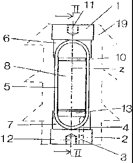
suppressor which is illustrated in Figures 1 to 3 has
two connecting fittings l, 2, which are preferably
composed of aluminum and are spaced apart from one .
another along an axis z. The connecting fitting 1 is
i5 provided with a fastening device, which~is designed as
a~threaded hole 11, for an electrical conductor which
may be connected to high-voltage potential, but is not
illustrated. The connecting fitting 2 may be Connected
to ground potential by a fastening device which is
designed as a threaded hole 12. Said cbnnecting fitting
,~~2 has' an axially aligned threaded hole 3 in which~a
pressure screw 4 is guided such that it can be
displaced in the axial direction. The designation 5
refers to a loop composed of a wound, glass-fiber
reinforced strip which is embedded in a plastic matrix.
The two ends ~of the loop 5 are guided in sections,
which are designed in the form of slots, of material
cutouts 6, 7 which are formed in the connecting
fittings 1, 2.
, A ,cylindrical varistor element 8 composed of
non-linear resistance material; for example based on
metal oxide such as Zn0 .in particular,, is arranged
;betwe,en the connecting fittings 1,, 2 ; forming a
' suppressor active. part in the form of a column.
~35 Alternatively, two or more varistor elements, which are ~. '
stacked one above .the other in the form of a column,
may also be provided instead of,one element 8: . '
Electrically, conductive, parts, namely two .
spring elements 9, which produce contact pressure and
- CA 02202967 1997-04-17
. _ - 4 - 96/076
are ~in eachcase designed as plate springs, and a
' .thrust' washer 10, which is preferably composed of
aluminum, copper or an aluminum or, copper allay, are
. mounted such that they can be displaced in the axial
direction in a cutout which is~ in the form of a disk
y. "and ~is formed in the connecting fitting 1 (Fig. 2) . A
,thrust washer. 13,. which is composed of the same
material as the part 10, is likewise mounted such that
it can be displaced in the. axial direction in a.cutout,
which is in the form of a disk, in the connecting
fitting 2 (Fig. 2). Current transmission elements'.14
are arranged between the thrust washer 10 and the
varistor element 8, and between the thrust washer 13
and ,the varistor element 8, and are in each case
designed as a disk with grooves which pass
concentrically around~the axis and are formed in both
end surfaces of the disk (Fig. 3): The current
transmission elements 14 are advantageously formed from
annealed aluminum.
Fig. 2 shows that each of the sections which
are marked by the designations 15, 16 and are in the
form of slots extend essentially transversely with
respect .to the axis z from the outer surface of~ the
' electrical connecting fitting 1 or 2, respectively, to
beyond the axis z. Each of the two ends of the loop 5
is inserted beyond the axis z into the section 15 or
16, respectively, which is in the form of a slot,' and
in each case rests on a surface 17 or 18, respectively,
which bounds the section 15 .or 16, respectively, which
, is in the form of a slot (Fig. 3). This ensures that,
the loop 5 is held centrally in the region of the axis .
z, and ensures a uniform, contact pressure in the
1 suppressor active part. This ensures a uniform .current
w density.of the suppressor current which is carried in
35, the suppressor active part when an overvoltage occurs.
.At the.same time, unacceptably high local heating in,
the~'suppressor active part is avoided. ~ -w
Increased confidence. against displacement of
the loop transversely with respect to the axis z is
v
CA 02202967 1997-04-17
- 5 - 96/076
provided if the slots 15, 16 are inclined by somewhat
more, than 90°, for example by up to 95° with respect to
the axis, and/or if the slots 15, 16 have undercuts
. which fix the loop ends and can be formed in the
contact surfaces 17, 18.
The contact surfaces 17, 18 advantageously have
a surface profile which is essentially in the form of a
circular. arc. The loop ends then rest on. the connecting
fittings 1, 2 with a, uniform, relatively slight
curvature. This largely avoids undesirably high bending
and shear stresses in the loops. ~ .
A rectangular, in particular square, cross-
sectional profile of the loop 5 with a relatively
narrow width transversely with respect to the axis z is
particularly advantageous since the section 15 or 16,
respectively, which is designed in the form of a slot,
need extend only insignificantly beyond the axis z. The
connecting fitting 1 ,or. 2 then has high mechanical
strength. '
2p The connecting fittings 1, 2 are partially ,
enclosed, and the varistor element 8, the thrust plates
10, 13 and the loop 5 are completely enclosed, by a
molded housing 19 which is provided with shields and is
made of insulating material, preferably of an.
elastomeric silicone (Fig. 1).
In order to produce this, overvoltage
suppressor, the connecting fitting 2, the thrust plate
13, one of.the current transmission elements 14, the
varistor element 8, a further current transmission
element 14, the thrust plate° 10, the two spring
elements 9 and the connecting fitting 1 are stacked one.
- above the other in sequence in a template, and are '
subjected to a prestressing force. The connecting
' ,.fittings 1, 2 are , in this case aligned ,such that, the .
two sections~l5, 16,, which are in the form of slots,
are located one. above the other such that they are
superimposed (Figures 2 and 3). A prefabricated loop 5, , ,
which is preferably composed of a wound prepreg which '
is in the form of a,strip.and has been cured after
CA 02202967 1997-04-17 .
- 6 - 96/076
winding, is then, pushed so far into the slots 15, 16
that the axis, z passes through the loop ends_ The
prestressing force is then removed, and the suppressor
active part is~ thus complete. Contact and retention
force. can additionally be produced in the suppressor
active part by twisting the pressure screw 4:
Instead of a prefabricated loop, a loop can
also be used which is formed during the production of
' ,the overvoltage suppressor. To this end,,a strip which
is subjected to a prestressing force is wound around
the suppressor, active part and is placed on the two
contact. surfaces 17,' 18. In this case, the two
. connecting fittings l, 2 are braced firmly to one
another' forming a contact force, and a mechanically
robust active part of the overvoltage suppressor to be
produced is thus formed.. This bracing is in general
completely sufficient on its own for good mechanical
strength of .the suppressor active part. If a strip
having adequate elasticity is used, such as a strip
manufactured from glass fibers for example, the spring
elements 9 may thus possibly be omitted.
Such a strip is preferably- a prepreg,
particularly based on glass fibers and epoxy resin. A
~prepreg has a good,adhesion effect. A loop which ~is
' wound from'a ~prestressed prepreg is thus robust even
without any additional fastening device after winding,
and can then be cured at elevated temperatures . A loop
is then formed in this case which ~is composed of glass
' fibers and a cured plastic matrix in which the glass
fibers are embedded.
In addition to making good contact with the
individual parts which are located in. the current path
betweeri the two connecting fittings; the bracing of the,
. two connectings fittings 1, 2, at the same time ,also
results'in the grooves of. the current transmission
elements l4 being closely joined at the end surfaces of
the' varistor, element 8 andvof the thrust washers 10,
13. I,f the . suppressor .active part is subsequently
' extrusion coated with insulating material, preferably
CA 02202967 1997-04-17
- 7 - 96/076
based on an elastomeric silicone, this avoids ingress
of the liquid insulating material between the
individual parts located in the current path.
Obviously, numerous modifications and
variations of the present invention are possible in
light of the above teachings. It is therefore to be
understood that within the scope of the appended
claims, the invention may be practiced otherwise than
as specifically described herein.