Note: Descriptions are shown in the official language in which they were submitted.
CA 02203430 1997-04-22
WO 96/17267 PCT/US95tl4608
METHOD AND APPARATUS FOR FORMING A CONTOURED
PLANARIZING LAYER FOR A COLOR FILTER
RELATED APPLICATIONS
This application is a Continuation-ln-Part of United States Patent
Application 08/348,597, filed on December 2, 1994, titled "Method and
Apparatus for Forming a Contoured Planarizing Layer for a Color Filter."
0 FIELD OF THE INVENTION
The invention relates to color filters for liquid crystal display panels, and
methods for their production.
BACKGROUND OF THE INVENTION
Liquid crystal display panels (LCDS), particularly color LCD panels, are
used for flat screen televisions, projection television systems and camcorder
view finders, with many more applications anticipated in the future.
The fabrication of an active matrix liquid crystal display involves
preparation of a front and rear glass panel. Preparation of the front glass panel
involves deposition of a color filter element onto a suitable substrate, such asglass. Color filter deposition typically involves depositing a black matrix pattern
and three primary (typically either red, green and blue or yellow, magenta and
cyan) color dot or color cell patterns within the spaces outlined by the black
matrix. The lines which form the black matrix typically are about 15-25 microns
wide and about 0.5 to 2 microns thick. The red, green, and blue color cells are
typically on the order of about 70-100 microns in width by 200 to 300 microns in
CA 02203430 1997-04-22
WO 96/17267 PCI/US95/14608
length. The printed color cells are typically less than about 10 microns thick,
and preferably less than 5 microns thick, and must be evenly applied and
accurately registered within the pattern formed by the black matrix. The front
glass substrate is typically completed by depositing a planarizing layer, a
transparent conducting layer, and a polyamide alignment layer over the co~or
filter element. The transparent conducting layer is typically indium tin oxide
(ITO), although other materials can also be utilized.
Preparation of the rear glass panel involves formation of thin film
transistors or diodes, as well as metal interconnect lines. Each transistor actsas an on-off switch for an individual color pixel in the display panel. The third
and final step is the assembly of the two panels, including injection of a liquid
crystal material between the two panels to form the liquid crystal display panel.
One aitical step in color filter formation is the formation of the red, green
and blue color dots (also referred to as color cells) of the color filter. Such color
cells preferably should be deposited so that they are as smooth and uniform in
thickness as possible. Previous ink printing methods used to print color filter
patterns have resulted in color patterns having insufficient smoothness. This islargely because the ink depositing methods of the prior art resulted in ink cells
which were rounded or triangular in cross section. Consequently, a planarizing
layer is commonly applied over the color patterns, after they have been printed
onto a substrate, to alleviate imperfections in coating smoothness or thickness
uniformity due to the deposition process. The transparent planarizing layer alsoserves to protect against ion migration to and from the ITO layer and color
pattern layer. The planarizing layer should be deposited to be as smooth and
2s flat as possible.
Previously, a new method for providing such protective planarizing layers
has been proposed by Corning Incorporated. This new method has been the
subject of a patent application S.N. 08/197,141, filed February 16, 1994, entitled
"Color Filters and Method of Printing", the specification of which is hereby
incorporated by reference. In that application, a transfer layer 14 is provided
onto a collector 16. Afterwards, the ink color cells are deposited using ink
printing methods onto the transparent transfer layer. The ink color cells are
CA 02203430 1997-04-22
W O 96/17267 PCTAUS95/14608
then deposited onto a glass substrate, and sandwiched between the transrer
layer and the glass substrate, in a process similar to that illustrated in Fig. 3.
After a planarizing layer has been deposited, a conductive layer such as
indium tin oxide (ITO) is typically deposited over the planarizing layer. If theoutside top or upper edges of the pla~ ,ari~ing Iayer have sharp or square (90
degrees) edges, breaks or discontinuities can occur in the conductive (ITO)
layer which is deposited over the planarizing layer. Consequently, it would be
desirable to provide a method and apparatus for making color filters which is
capable of producing planarizing layers which do not have sharp edges and
therefore do not result in breaks in the ITO layer. It would further be desirable
to produce such color filters using a method which is simpler and more efficientthan prior art methods.
In addition to the ability to provide tapered or radiused edges on the color
filters, it would also be desirable to be able to produce other contoured shapeson the planarizing layer or other top protective layer which is deposited over the
color filter. For example, it would be desirable to be able to impart a
microgroove patler~ on the surface of the top protective layer. Such
miaogroove patterns can be used to orient the liquid crystal without the need for
a separate alignment layer. Such microgroove patterns are discussed, for
example, in "Regularity and Narrowness of the Intervals of the Microgrooves on
the Rubbed Polymer Surface for LC Alignment" by Ito et al., SID 1992 digest,
pages 393-396 (1992).
SUMMARY OF THE INVENTION
The present invention relates to methods for forming contoured
planarizing layers on color filters for liquid crystal display applications, by
forming the planarizing layer on a contoured collector device prior to deposition
to a substrate. A transfer layer is provided on the contoured collector device,
such as, for example, a collector roll or collector plate. The individual red,
3 o green, and blue color cells which make up the color filter are then deposited on
the transfer layer to form a color filter pattern. Preferably, a black matrix pattern
is formed on the transfer layer prior to the colored ink cells. After formation of
CA 02203430 1997-04-22
WO 96/17267 PCT/US95/14608
the color pattern on the transfer layer, the entire composite of transfer layer and
color filter pattern is transferred from the collector device to the substrate so that
the coior filter pattern contacts the glass substrate. The trans~er layer thus ends
up on top of the color filter pattern, and thereby serves as a planarizing and/or
protective layer for the color filter.
Because the collector device employed in the present invention has a
shaped or contoured surface, this contoured shape is imparted to the
planarizing layer. Thus, if desired, a beveled or raised shape may be provided
along the outside edges of the transfer layer by employing an appropriately
shaped collector surface. In such cases, when the transfer layer is deposited
onto the glass substrate (preferably along with the color cells which make up the
color filter), the lra"srer layer serves as a planarizing and/or protective layer
having a beveled or raised outer edge which slopes downwardly toward the
outer edge of the glass substrate. To facilitate formation of the tapered regionlS down to the glass substrate, the transfer layer is preferably sandwiched, during
its formation, between the contoured collector roll and another roll having a
relieved region on its outer periphery which approximates the depth of the colorfilter pattern. The relieved region on this roll forms an upraised region on thetransfer layer directly opposite the taper edge region of the transfer layer. The
color filter pattern is then deposited on the transfer layer within this upraised
region of the transfer layer. In this way, the tapered edge region will surroundthe color filter pattern, and the color filter pattern will seem to be embedded
within the transfer layer.
In one such embodiment of the present invention, prior to receiving the
color cells which make up each pixel of the color filter, a transfer layer is
deposited onto a contoured collector roll having a recessed central portion and
outer edge beveling portions. The transfer layer is then contacted with a black
matrix patterning roll which has a recessed pattern thereon which corresponds
to the desired black matrix pattern. Preferably, this recessed pattern contains
black matrix ink. and the black matrix ink is cured, or at least partially cured,
prior to or during deposition to the transfer layer, to help retain the shape of the
intaglio recessed pattern. Transfer of this cured black matrix pattern results in
CA 02203430 l997-04-22
WO 96/17267 PCT/US9~/14608
the fo-."ation of a raised black matrix pattem on the trai,srer layer. Preferably,
the raised black matrix pattem is about 1 to 10 microns thick, more preferably
about 2 to 6 microns thick, and most preferably about 3 to 4 microns thick above the remainder of the transfer layer.
Ink in intaglio and gravure print plates typically has a negative
meniscus, the surface of the ink in the recessed intaglio pattern curving below
the print plate surface. Conse~uently, the transfer layer is preferably liquid
when it contacts the black matrix ink, so that it can adhere to the black matrixink. The portion of the liquid transfer layer which contacts the black matrix ink is
preferably cured while in contact with the black matrix ink and thereby removes
the ink from the recesses of the intaglio print pattern. The region of the transfer
layer corresponding to the outer edges of the resultant color filter (i.e., the
tapered edges) is preferably masked so that it is not cured during this step, but
rather remains liquid or tacky so that it will subsequently adhere to the substrate
during a later transfer step.
The black matrix patterning roll may alternatively be employed without
black matrix ink, and the recessed pattern utilized to deform the color filter side
of the transfer layer according to the black matrix ink pattern, to thereby form a
raised pattern corresponding to the desired black matrix pattern. Such
embodiments are unique in that both sides of the planarizing layer are being
formed or shaped before the planarizing layer is deposited onto a color filter
pattern substrate. The portion of the transfer layer contacting the patterning
surface of the pattern roll is preferably cured, during the contacting step, so that
the transfer layer permanently retains the pattern imparted by the roll. The red,
green, and blue color dots are then deposited within the recesses of the raised
pattern formed on the ~(ansfer layer. If desired, a black matrix ink pattern can be
deposited on top of the raised pattern or at another location within the liquid
crystal display device. For example, the black matrix pattern could be depositedon the TFT substrate on top of the thin film transistor.
Ink printing methods are employed to deposit the red, green and blue
color cells within the recesses formed by the raised pattern (which preferably is
a raised black matrix pattern). Then, while the ink which makes up the color
CA 02203430 1997-04-22
WO 96/17267 PCT/US95/14608
cells is still deformable, the resulting composite, which consists of the transfer
layer, the color ink cells, and optionally a black matrix pattem, is transferred to
the glass substrate. The soft, deformable color ink cells are compressed
between the transfer layer and the glass during this deposition step. Because
s the color cell inks are plastically cJefor")able during deposition to the substrate,
they are compressed to a smoother, more uniform thickness and a smoother,
more flat top than has been possible using prior art methods. The transfer layeraides in the deforming of the color ink, and also serves as a planarizing or
protective layer, thereby helping to retain the more uniform ink cell shape. In
this regard, the present invention is conlrary to the prior art, wherein color filter
arrays were deposited onto a substrate first, followed by deposition of a
planarizing layer and then a smoothing process in subsequent process steps.
The colored ink cells and the remainder of the transfer layer (e.g. the region
corresponding to the outer edges of the color filer) are preferably sufficientlyhardened during transfer, or soon thereafter, to adhere the ink and transfer layer
composite to the substrate and, at the same time, permanently retain the
flattened shape of the color ink dot. This can be achieved, for example, by
utilizing radiation curable inks and curing the ink simultaneous with the
compression transfer. Adhesion to the glass substrate is provided by the pixel
inks and that portion of the transfer layer that contacts the substrate (generally
outside the color pixel ink regions), both of which are preferably cured by UV
exposure while under compression during the final transfer. For tapered edge
transfer or planarizing layers, the edge region of the transfer layer beyond
where the pixel inks are printed will provide adhesion, provided this region
retains sufficient tack to adhere to the substrate.
The transfer layer may be formed using, for example, those materials
selected from the group consisting of polyimides, epoxides, acrylics, vinyl
ethers, polyurethanes, polyesters, and acrylated or methacrylated acrylics,
esters, urethanes, or epoxides, and other materials which are conventionally
useful as planarizing layers in conventional color filter devices. A preferred
material for the transfer layer is a radiation curable acrylate material, such as a
radiation curable epoxy acrylate. The transfer layer is deposited onto a
CA 02203430 1997-04-22
WO 96/17267 PCT/US95/14608
collector device as a thin film, typically less than 10 microns. Preferably, thetransfer layer is formed of a radiation curable material to facilitate curing. !n
such cases, the majority of the transrer layer is cured while receiving the ink
pattems which make up the black matrix and color filter paller"s. For taper
s edged transfer layers, the taper edge regions are preferably protected from
curing radiation while receiving the ink pattern, so that they remain liquid until
deposited to the substrate. These edge regions are then cured, along with the
color ink dot pattern, during deposition to the substrate.
The present invention has several advantages over prior art methods. By
tapering the edges of the transfer layer, breaks in the conductive film (which is
typically ITO)are avoided. Because the planarizing layer is applied to the colorfilter during the color filter deposition process, no subsequent forming process is
needed to apply or taper the outer edge of the planarizing layer.
By employing a smooth collector surface, the transfer layer will end up as
a smooth top planarizing layer. However, it may be desirable in some cases for
the transfer layer to be other than planar or smooth. In these cases, the desired
topography can be imparted by first forming the inverse of the desired
topography on the collector surface. For example, by appropriately shaping the
collector roll to have a microgroove pattern thereon, the microgroove pattern will
be imparted into the top of the transfer layer when it is deposited on the
substrate. Such "microgroove" texture surfaces can be used to orient the liquid
crystal material without the need for a separate alignment layer. Before the
present invention, microgroove patterns were typically formed on the top layer of
color filters using rubbing or abrasion techniques.
By microgroove pattern, it is meant that, for example, a plurality of
parallel ridges or grooves are provided on the collector roll surface. These
parallel microyrooves can be, for example, on the order of ten ridges or groovesper one micron length of collector roll surface, the ridges being approximately
seven hundredths to several tenths of a micron high. Of course, if desired, the
3 o microgrooves can be smaller or larger, or more or less disperse than these dimensions.
CA 02203430 1997-04-22
W O96/17267 PCTrUS95/14608
BRIFF DESCRIPTION OF THE DRAWINGS
Figure 1 illustrates a method and apparatus in accordance with the
present invention.
Figure 2 illustra~es an alternative method and apparatus in accordance
with the present invention.
Figure 3 illustrates the deposition of a transfer layer, along with a black
matrix pattern and color ink dot pattern, to a glass substrate.
Figure 4 illustrates a preferred embodiment of the present invention.
Figure 5A is an axial cross-sectional view of a collector device, in
accordance with the present invention, having a transfer layer thereon and
receiving a black matrix pattern in accordance with the process illustrated in
Fig. 1.
Figure 5B is an axial cross-sectional view of the deposition of a transfer
layer, black matrix pattern, and color filter array composite from a collector roll to
a substrate in accordance with the present invention as illustrated in Fig. 3.
Figure 5C is a cross-sectional view of a resultant color filter formed using
the processes illustrated in Figs. 5A and 5B.
Figure 6A is a cross-sectional view of an alternative collector roll in
accordance with the present invention.
Figure 6B illustrates a cross-section of the resultant color filter and
planarizing layer formed utilizing the collector roll illustrated in 6A.
Figure 7A is a cross-sectional view of an alternative collector roll in
accordance with the present invention.
Figure 7B illustrates a cross-section of the resultant color filter and
planarizing layer formed utilizing the collector roll illustrated in 7A.
Figure 8A is an enlarged partial perspective view of a collector surface
having a microgroove pattern thereon.
Figure 8B is a perspective view of a color filter having a microgroove
3 o surface as a result of being deposited by the collector surface illustrated in
Figure 8A.
CA 02203430 1997-04-22
W O 96/17267 PCTrUS95/14608
Figure 8C is an enlarged partial perspective view of a collector surface
having a ,~referred microgroove pdller~, thereon.
DETAILED DFscRlpTloN OF THE INVENTION
s In the present invention, a t~ansfer layer is deposited onto a collector
device, such as a collector roll or collector plate. The collector devices in
accordance with the present invention comprise a contoured surface thereon so
that, when the transfer layer is transferred from the collector device onto a
substrate, the upper surface of the transfer layer is shaped according to the
contoured sufface of the collector device. Thus, for example, the method of the
present invention can be employed to make planarizing layers having tapered
outer edges.
The red, green and blue color dot patterns are then deposited on the
trd,1~rer layer, and the resultant composite, which consists of the transfer layer
and color cells, is transferred in one step to the glass su~strate. Prior to
receiving the color dot patterns, a black matrix pattern is preferably deposited onto the transfer layer.
The transfer layer provides a unique surface on which to form each of
the red, green and blue (or yellow, magenta, and cyan) color dot patterns and, if
desired, the black matrix ink pattern. Forming the color filter pattern on a
transfer layer enables the entire assembly, consisting of the transfer layer, black
matrix pattern and color dot patterns, to be transferred to a substrate so that the
color hlter is sandwiched between the transfer layer and the substrate. Because
the transrer layer acts as an in-situ formed planarizing layer, no subsequen
operation is needed to form a planarizing layer. Such transfer layers are further
discllssed in United States Patent Application No. 08/197,141, the specificationof which is hereby incorporated by reference.
In one embodiment of the present invention, the transfer layer is applied
onto a collector surface having a slightly recessed central portion which tapers3 o radially outwardly from the surface of collector roll as one travels axially toward
the outside edges of the collector roll. In Figs. 5A and 6A, for example, the
collector roll 16 illustrated has recessed central portions 70. Outwardly from
CA 02203430 1997-04-22
WO 96/17267 PCT/US95/14608
these central portions (i.e., from the center of the roll), the surface of the
collector roll 16 angles radially outwardly from the axis of the collector roll to
form bevel forming regions 72. Utilizing the recessed collector surface
illustrated in Figure 5A and 6A, the transfer layer is deposited onto the collector
surface, after which the color cells which make up the color filter are deposited
on the transfer layer prior to transfer to the substrate. Preferably, the black
matrix ink pattern is also deposited on the transfer layer (as illustrated in Figs. 1
and 5A, and as will be further explained hereinbelow), prior to receiving the
color cells. The entire composite can then be deposited, with the transfer layeron top, to form a color filter suitable for use in liquid crystal displays. In this
way, the transfer layer will become the planarizing layer. The outer edges of the
tapered transfer or planarizing layer are preferably formed so that the taper
extends around the edges of the color filter pattern. For example, in Fig. 5a, the
outer edges of the transfer layer are formed between the edge tapering region
72 of collector roll 16 and a relieved region 73 which is on black matrix
patterning roll 18. The relieved region 73 forms upraised region 78 on transfer
layer 14. This upraised region 78 will in effect surround the color filter pattern
and contact the glass substrate when deposited thereto. Utilizing the collector
roll 16 in conjunction with the black matrix patterning roller 18 illustrated in Fig.
5A will result in the formation of the tapered planarizing layer illustrated in Fig.
5C, wherein the bevel forming regions 72 of collector roll 16 form beveled or
tapered regions 74 on planarizing layer 14.
Likewise, utilizing the collector roll 16 illustrated in figures 6A will result in
the formation of a planarizing layer having radiused taper edge regions 74, as
illustrated in Fig. 6B.
The collector roll 16 illustrated in Figure 5A and 5B utilizes a distinctly
angled taper, while the collector roll 16 illustrated in Figure 6A utilizes a
rounded or radiused taper. Such rounded or angled tapers can employ a wide
variety of angles. Preferred taper angles include, for example! from about 20
to 70, and more preferably from about 30 to 45 . It should be noted, however,that the invention is not limited to these particular angles, and that virtually any
angle desired could be employed.
CA 02203430 1997-04-22
WO 96/17267 PCT/US95/14608
The contoured collector roll 16 of the present invention is not limited to
providing angled or rounded tapers to planarizing layers, but also could be
utilized to form a textured surface on the top of transfer layer 14. For example,
any of the collector rolls 16 discussed herein can be provided with a surface
s having grooves or ribs 75 thereon which are substantially parallel to one
another, as illustrated in Figure 8A. In this way, the resultant planarizing layer
14, as illustrated in Fig. 8B, will have corresponding grooves or ribs 77 provided
thereon.
Preferably, the grooves or ribs 75 are straight and parallel to one
another, as illustrated in Figure 8C. In this way, the resultant planarizing layer
14 will have cor~asponding grooves or ribs 77 provided thereon which are also
straight and parallel to one another.
Fig. 1 ill~.s~rates an axial cross-sectional view of a process in accordance
with the present invention. It should be noted that, to facilitate explanation of
lS the present invention, none of the drawings discussed herein are necessarily of
realistic comparative dimensions. Transparent transfer layer 14 is provided on
collector roll 16. Collector roll 16 has a contoured surface. By contoured, it is
meant that the peripheral surface is not flat (i.e., not perfectly cylindrical). For
example, a collector roll such as the one illustrated in Figs. 5A or 6A could beused to form a planarizing layer having tapered outer edges. In addition to the
bevel forming regions 72 illustrated in Figs. SA, 6A, or 7A, as illustrated in Fig.
1, similar bevel forming regions 72 can be provided to bevel the leading and
trailing edges of the planarizing layer. Alternatively, or additionally, collector roll
16 can be provided with ridges or grooves, as illustrated in Fig. 8A, so that the
transfer layer 14 is in turn provided with a corresponding grooved pattern, as
illust,a~ed in Figure 8B.
In Fig. 1, intaglio roller 18 is used as a black matrix ink patterning roll, in
that it has an ink receiving recessed pattern 20 thereon which receives radiation
curable, thermal wax, or solvent based black matrix ink 28. In a preferred
embodiment, ink applicating roller 30 applies radiation curable black matrix ink28 into recessed pattern 20. Excess ink is removed from the pattern 20 by
doctor blade 32. The ink is then cured or set within recessed pattern 20, such
CA 02203430 l997-04-22
WO 96/17267 PCT/US95/14608
12
as, for example, by exposure to ultraviolet radiation from UV lamp 34, thereby
forming a black matrix pattern 10 which will at least substantially retain the
shape of the recessed pattern 20. Alternatively, in a preferred embodiment,
intaglio roll 18 is constructed of radiation transparent material, and a UV light
34c is mounted therein to cure the black matrix ink while it is retained within
recessed pattern 20. Such curing or setting of the black matrix ink can
alternatively take place simultaneous with contact of the black matrix ink with the
transfer layer. For example, the black matrix ink could be cured by radiation
from UV light 34a, located within collector roll 16. When the curing or hardening
of the black matrix ink is accomplished, the black matrix will retain the exact
shape of recessed pattern 20. Black matrix patterning roller 18 is contacted with
transfer layer 14 to transfer the cured or otherwise hardened black matrix
pattem 10 from recessed pattern 20 of patterning roller 18 to transfer layer 14
on collector roll 16.
Transfer layer 14 may be applied using ink-type applicating rollers, as will
be further discussed below. Transfer layer 14 may be partially cured prior to
receiving the black matrix pattern. However, transfer layer 14 is preferably
liquid and smooth prior to contacting the black matrix pattern. Ink in intaglio and
gravure print plates typically has a negative meniscus, the surface of the ink
curving below the print plate surface. Consequently, the transfer layer must be
sufficiently sofl and tacky to adhere to the black matrix ink and remove the inkfrom the recesses of the intaglio print pattern. The portion of the transfer layer
that contacts the black matrix is preferably cured during the transfer of the black
matrix pattern to transfer layer 14. Such curing may be accomplished by
utilizing ultraviolet radiation curable material to form transfer layer 14, and
applying radiation, via ultraviolet (UV) light 34a, to transfer layer 14 during
deposition of the black matrix pattern 10 to transfer layer 14. Although the UV
light can be transmitted in a variety of ways, including through the collector,
through the black matrix intaglio plate. or by focusing in the trailing (separation)
nip between both, in a preferred embodiment the UV light 34a is mounted within
collector roll 16, which is made of UV radiation transparent material to allow the
radiation to be emitted therefrom. It should be noted that the radiation
CA 02203430 1997-04-22
WO 96/17267 PCT/US95/14608
13
employed does not have to be ultraviolet, but could instead be visible, inr, ared,
or other radiation, depending on the photoinitiator employed for the transfer
layer.
Adhesion to the glass subsl-ate is provided by the pixel inks which, for
s example, can be cured by UV exposure while under con,pression during the
final tra"srer. For taper edged transfer layers, the edge region of the transferlayer beyond where the pixel inks are printed can also provide some adhesion,
provided the l,dnsrer layer retains sufficient tack or liquidity at this process step
to adhere to the glass. Consequently, as illustrated in Figs. 1 and 5A, the
portions of the transfer layer outside the color filter pattern (e.g., all portions
adjacent to edge taperin~ regions of collector roll 16) preferably are masked byshadow masks 76 during the curing step used to cure the transfer layer to the
black matrix ink. The remainder of the transfer layer (the edge pattern around
the color filter) remains liquid and is subsequently cured during the final transfer
of the composite to the substrate along with color pixel inks, as illustrated in Fig.
5B.
Using the embodiment illustrated in Fig. 1, v,/herein the black matrix
pattern is cured while in the recessed pattern of intaglio roller 18, the resolution
of the black matrix pattern is dependant upon the depth and shape of recessed
pattern 20 and how well this shape is imparted to the black matrix pattern 10.
By setting or curing black matrix pattern 10 while it is still contained within
recessed pattern 20, the black matrix pattern will necessarily acquire the square
edges and corners of the recessed pattern, thus avoiding the jagged, triangular
or rounded corners and edges which are typical of conventional ink printing
2 5 techniques.
Alternatively, the apparatus illustrated in Fig. 1 could be used to contour
the color filter side (i.e., the side which contacts the colored inks which make up
the color filter) of the transfer layer, rather than deposit the black matrix thereto.
To do so, intaglio roll 18 can be utilized without ink 28 so that the recesses 20
deform the transfer layer 14. Fig. 2 illustrates this alternative method in
accordance with the present invention. Recessed pattern 20 on roller 18
corresponds to the desired black matrix pattern. Consequently, the resultant
CA 02203430 l997-04-22
WO 96/17267 PCT/US95/14608
14
raised pattern 22 formed on transfer layer 14 by contact with the recesses 20
will correspond to the desired black matrix pattern 10. Transfer layer 14 will
have to be hardened sufficiently to retain the embossing pattem obtained from
roll 18. This can be accomplished by utilizing thermoplastic inks and cooling the
transfer layer, at the point of contact with roll 18, to set the ink. Alternatively,
and more preferably, radiation curable inks are employed, and radiation is
emitted from ultraviolet light 34a through collector roll 16 to cure the transfer
layer 14 during the embossing operation. In accordance with the present
invention, collector roll 16 is again a contoured roll, such as, for example, isillustrated in Figs. 5A, 6A, 8A or 8C. If a taper edged collector roll 16 is
employed, it preferably is masked, as explained above with respect to Fig. 5A,
to protect the taper edges from being cured during the transfer of the black
matrix pattern to the transfer layer. Thus, while the contoured surface of
collector roll 16 shapes one side of transfer layer 14, the other side of transfer
layer 14 is shaped by recessed pattern 20 of intaglio roller 18. Consequently,
this particular process is especially unique, in that both sides of the planarizing
layer would be contoured or shaped before the planarizing layer was deposited
onto a substrate. If desired, black matrix ink may be applied from black matrix
ink applicator roll 30 to upraised pattern 22 to form raised black matrix pattern
10.
Alternatively, the black matrix ink 28 can be applied at a different location
in the process of manufacturing the liquid crystal display panel. For example,
the black matrix ink can be applied on the other (TFT) glass substrate. If
desired, for example, the black matrix pattern can be deposited on top of the
thin film transistor. For applications in which the black matrix pattern is
deposited on the TFT substrate, it is felt that formation of the raised pattem 22
on transfer layer 14 is advantageous, in that it separates and aligns the various
color cells with the black matrix pattern. By then registering the black matrix
pattern 10 to be aligned with raised pattern 22, when one looks down at the
3 o resultant liquid crystal display, the color cells will appear to be within the black
matrix pattern.
CA 02203430 1997-04-22
WO 96/17267 PCT/US95/14608
Completion of the color filter involves formation of the color pixels. Each
color pixel typically consists of a red, green, and blue subpixel (subpixels arealso herein referred to as color cells). In all of the above described
- embodiments, after the raised pattem 22 (or raised black matrix pallerr, 10) has
5 been applied to transfer layer 14, the red, green and blue color cells of the color
hlter pattern are applied to transfer layer 14 within the recesses 11 formed by
raised pattern 10. Preferably, the red, green and blue color cells are depositedwithin black matrix pattern 10 using typographic ink printing techniques. After
deposition of the red, green and blue color ink cells within raised pattern 10, the
entire composite, which consists of transfer layer 14, raised pattern 10, and red,
green and blue color cells 36, is transferred to a glass substrate 12.
Fig. 3 illustrates the deposition of a black matrix pattern 10, color filter
pattern 36, and transfer layer 14 from collector roll 16 to a glass substrate 12.
Collector roll 16 again employs a contoured surface such as is illustrated in
Figs. 5A, 6A, 8A, 8C or some other contoured surface. The composite
illustrated in Fig. 3 consists of black matrix pattern 10 formed using the method
illustrated in Fig. 1, as well as the color ink cells 36 which comprise the color
filter pattern. During deposition of the composite to the substrate, the ink cells
36 which comprise the red, green and blue color cells are preferably in a liquidor otherwise deformable state. Consequently, the ink cells are squeezed, during
the deposition, between transfer layer 14 and glass substrate 12, and thereby
deformed to a smoother, more uniform ink dot shape and thickness. This more
uniform shape and thickness is retained, preferably by curing simultaneous to
the transfer operation. Such curing can be accomplished via UV light 34d,
which is positioned to emit radiation through the glass substrate, as illustrated in
Fig. 3 and Fig 5B. In addition to curing the deformable color ink dots, the taper
edges (if formed) are also preferably cured at this time. Such a curing operation
is best illustrated in Fig. 5B, which slows UV light being emitted from UV light
source 34d to simultaneously cure the color ink cells 36 and the outer edge
regions of transfer layer 14.
Figure 4 iliustrates a preferred apparatus for carrying
CA 02203430 1997-04-22
WO 96tl7267 PCTIUS95/14608
16
out the method described above with respect to Figs. 1 and 3. The Fig. 4
apparatus includes l,ar,srer layer applicator roll 42, which applies a relatively
uniform thickness transparent
transfer layer 14 to collector roll 16 prior to receiving the
s multicolored ink pattern. Collector roll 16 has a contoured surface thereon. For
- example, the contoured collector roll 16 can be designed like the collector roll
surfaces illustrated in Figs. SA or 6A to produce a planarizing layer having
tapered outer edges, or like 8A to produce a microgroove pattern, or a
combination of such contoured collector surfaces.
0 After the formation of transfer layer 14, a raised black matrix pattern is
deposited from black matrix imaging roll 18 onto transfer layer 14. Black matriximaging roll 18 has a recessed pattern 20 thereon corresponding to the desired
black matrix pattern, and a relieved region 73 corresponding to the area of the
desired tapered region. Recessed pattern 20 receives black matrix ink from
black matrix inking roll 30. Excess ink is removed from recessed pattern 20 by
doctor blade 32 to provide a uniform thickness of ink within recessed pattern 20.
The black matrix ink is then at least partially cured or set while still contained
within recessed pattern 20 of black matrix imaging roll 18. This may be
accomplished by curing black matrix pattern 10 either prior to or simultaneous to
transfer to transfer layer 14. For example, in one embodiment, black matrix
imaging roll 18 is formed from a radiation transparent material, and an
ultra-violet light source 34c is provided within black matrix imaging roll 18 toemit ultra-violet radiation and thereby cure the black matrix pattern.
Alternatively, ultra-violet light source 49 may be positioned to emit ultra-violet
2s radiation onto the black matrix pattem roll 18 and thereby cure black matrix ink
pattern 10 while it is retained within the recessed pattern 20 of black matrix
patteming roller 18. Alternatively, the ink may set by appropriate cooling of a
thermal wax formulation, drying of a solvent based ink, or a combination of suchcuring mechanisms.
The cured black matrix pattern 10 is then transferred from black matrix
imaging roll 20 to transfer layer 14. The transfer layer 14 is preferably liquidprior to the deposition of the black matrix pattern thereon, so that it is tacky or
CA 02203430 1997-04-22
WO 96/17267 PCT/US9S/14608
17
sticky enough to remove the black matrix pattern from intaglio roller 18. While
in contact with the black matrix pattern 10, the transfer layer 14 is preferablycured or otherwise hardened so that it is sufficiently solid to substantially retain
its shape, and also so that it removes the black matrix pattem 10 from the roll
18. Such curing may be accomplished by designing collector roll 16 to be
transparent and emitting radiation from ultraviolet light 34a located within
collector roll 18. If the contoured collector roll 16 employs a taper edged
design, these taper edges are preferably masked from the UV radiation as
described above with respect to Figure 5B. The radiation emitted from UV light
34a cures ~ra~s~er layer 14. After the black matrix pattern has been formed on
l,d,lsrer layer 14, the red, green and blue color cell patterns which make up the
remainder of the color filter pattern are deposited on transfer layer 14. The
following is a description of how the red, green, and blue color cells are
deposited within the recesses 11 formed by black matrix pattern 10 on transfer
layer 14, all of which is supported by collector roll 16.
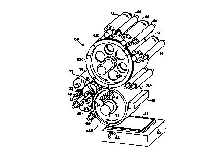
In the apparatus of Fig. 4, a single imaging pattern roll 50, having
multiple printing patterns thereon, is utilized to apply the red, green and bluecolor dot patterns. Pattern roll 50 may be virtually any form of roll capable ofproducing an ink pattem or image, including lithographic, typographic, waterlesslithographic, and so forth. Preferably, pattern roll 50 is a flexographic or other
type of typographic printing roll. Alternatively, the color may be transferred from
a typographic print plate rather than a roll.
In Fig. 4, pattern roll 50 is a typographic roll having three typographic
patterned ink receiving regions 52a, 52b, and 52c, thereon which receive ink to
form the blue, green and red color ink patterns, respectively. Inking rolls 54
apply the correct colored ink from ink metering rolls 56 to each of the three ink
receiving regions 52a, 52b and 52 of pattern roll 50. The inking rolls 54 are
movable to and from a contacting position with pattern roll 50, to enable each
colored ink to be applied only to the appropriate ink receiving region.
Collector roll 16 has two receiving surfaces: 58a and 58b. The separate
colored ink patterns developed on ink receiving regions 52a, 52b and 52c of
pattern roll 50 are printed onto receiving surfaces 58a and 58b of collector roll
CA 02203430 l997-04-22
WO 96tl7267 PCT/US95/14608
16 in registration. This means that each separate colored ink pattern from
region 52a, 52b and 52c prints its respective ink pattern on receiving surface
58a and 58b of collector roll 16 in a specific geometric relation with each of the
other colored ink patterns, each ink color being deposited within its respectives compartment within the black matrix pattern.
In Fig. 4, transfer layer applicator roll 42 is depositing a transfer layer 14
to receiving surface 58b of collector roll 16 and black matrix applicator roll 18 is
depositing a cured raised black matrix pattern 10 on transfer layer 14. Next, red
ink pattern region 52c will deposit the red color dot pattern onto receiving
surface 58b of collector roll 16, and green ink pattern region 52b will deposit the
green color dot pattern onto receiving surface 58a. On the next rotation of
collector roll 16, blue ink pattern region 52A will deposit the blue color dot
pattern onto receiving surface 58b, and red ink pattern region 52c will deposit a
red ink pattern onto receiving surface 58a. On the next rotation of roll 16, green
ink pattern region 52b will deposit a green color dot pattern onto receiving
surface 58b, and blue ink pattern region 52a will deposit a blue color dot pattern
onto receiving surface 58a. At this point, a complete color filter image will bepresent, with each of the colored inks deposited within the raised black matrix
pattern, all of which are on transfer layer 14, which in turn is supported by
receiving surface 58b of collector roll 16. The color filter image is inspected at
inspection station 60, which may employ, for example, an image analysis or
laser scanning type inspection system. If the multicolored pattern does not passinspection, it is rejected and cleaned off of compartment 58b by cleaning roller64. If the multicolored pattern passes inspection, glass substrate 12, which is
supported on vacuum chuck 62, is contacted with collector roll 16 and the
resultant composite, which consists of transfer layer 14, black matrix pattern 10,
and the red, green, and blue color cells, is transferred to the substrate.
Utilizing a method as illustrated by Figs. 14, the collector rolls illustrated
in Figs. 5A and 6A will result in color filter patterns such as those illustrated in
Figs. 5B and 6B, respectively. Figs. 5A and 6A illustrate collector rolls 16 forforming a single tapered color filter planarizing layer. Alternatively, the collector
roll 16 can be designed to produce planarizing layers for several different color
CA 02203430 1997-04-22
W O 96/17267 PCTrUS95/14608
filters at a time. For example, in the embodiment illustrated in Fig. 7A, the
collector roll 16 in,cludes two separate recessed regions 70a and 70b for
accepting the transfer layer, as well as bevel forming areas 72a, 72b, 72c, and
72d. Bevel forming areas 72a and 72b cooperate with recessed region 70a to
form a planari~ing layer 14a for a first color filter, while bevel forming areas 72c
and 72d correspond with recessed region 70b to form a planarizing layer 1 4b fora second color filter. In this way, two or more color filter patterns can be
produced using a single collector roll 16.
Transfer of the transfer layer/multicolored ink pattern composite from
collector roll 16 to the substrate preferably takes place while the multicoloredimage is still deformable. In this way, the inks are co",pressed, during the
transfer, between l(ansfer layer 14 and the substrate 12, as illustrated in Fig. 3.
In a preferred embodiment, the ink employed for the color ink cells is radiationcurable, vacuum chuck 62 is made of a transparent material, and an ultraviolet
light 63 is provided within vacuum chuck 62 to emit radiation through substrate
12. The ink is cured while under compression from the transfer deposition
operation, causing the ink cells to retain the more uniform shape created duringthe transfer operation.
Registration requirements for liquid crystal display color arrays is typically
on the order of plus or minus 30 microns, with future requirements expected to
be about plus or minus 5 microns. Because of these extremely demanding
registration requirements, a printing machine like that shown in Fig. 4, which
utilizes a single pattern roll 50 to form and deposit the various color patterns to
a single collector roll 16, is very useful.
In a preferred apparatus for carrying out the methods of the present
invention, the apparatus illustrated in Fig. 4 is mounted on its side (i.e., by
vertically mounting the printing rolls). By vertically mounting the printing rolls,
they may be removed vertically (in an axial direction, relative to the roll) from the
printing apparatus, as opposed to conventional horizontally disposed rollers,
which must be removed horizontally. In addition, if desired, the printing rolls can
be supported by a single bearing system located beneath each print roll, rather
than two (one at each end). Because this leaves the opposite end (i.e., the
CA 02203430 1997-04-22
W O96/17267 PCTAUS95114608
upper end) of each print roll free, these print rolls can be removed and replaced
by moving the rolls in a vertical direction. Consequently, changing print rolls is
greatly facilitated.
For e",bGdi,~)ents in which an ink (both black matrix and color ink) is
cured, the ink is preferably formulated to be radiation curable. By curable, it is
meant that the ink cross-links. By radiation curable, it is meant that the ink
cross-links when exposed to appropriate radiation. This is regardless of
whether the ink also has hot melt thermoplastic propenies in the uncured
(uncross-linked) state or incorporates a solvent. In the embodiment illustrated
in Fig. 4, vacuum chuck 62 is capable of transmitting radiation which is suitable
for curing the particular ink employed. For example, vacuum chuck 62 could
have an ultraviolet (1604001Jm) or visible (400-700,um) radiation source therein,
and thereby be capable of emitting ultraviolet or visible radiation. Altematively,
the ink can be exposed to the radiation by other methods, such as by aiming a
radiation source at the either at the trailing (separating) nip edge or compressed
nip region formed between the roll and the substrate. While such curing may be
done by radiation curing using conventional radiation emitting lamps,
alternatively a laser could be used, guided by mirrors. to cure (crosslink) the ink
sufficiently. In order for the dot to be cured in the deformed state by collector
roll 16 during deposition to the substrate, the surface area of the contact areabetween the collector roll and the substrate must be large enough, for a
particularly roll rotation speed, to allow for an appropriate amount of curing
while the dot is still being compressed in a flattened state. This contact area,called the "foot", is typically about a 5 to 25 mm wide contact area on the glass.
In carrying out the present invention, conventional radiation-curable inks
are generally preferred over thermoplastic inks, partly because they can be
printed at lower viscosities, which helps in printing the thin color cells. Also, it is
more difficult to control the pattern registration of hot melt thermoplastic inks, as
they require extremely tight thermal tolerances to control pattern dimensions. In
addition, radiation curable inks are easily cured during compression transfer
operations in accordance with the invention. Thermoplastic inks do have at
least one advantage, in that they can be formulated to set up immediately upon
CA 02203430 1997-04-22
W O96/17267 PCTAUS9S/14608
21
deposition to a sul~sl,~e or transfer roll having a lower temperature, resulting in
less pinholes, film non-uniformities and other such defects which can be r~ausedby inadequate wetting of transfer surfaces. Consequently, another pr~ferlad
type of ink is one that displays both thermoplastic and radiation curable
s properties. Such an ink is one which is formulated to be thermoplastic until
printed to the substrate, at which point it can be cured by exposure to
appropriate radiation. By cured, it is meant that the ink is to some extent cross-
linked. Cross-linking of the ink increases its durability and resistance to higher
temperatures, which is preferable due to the temperatures the color filter will be
exposed to in subsequent processing steps.
For the black matrix ink, another preferred type of ink is a solvent based
formulation in which a volatile solvent is incorporated into the ink to lower the
viscosity during inking and doctoring, the solvent being chosen so that it is
compatible with the ink and readily evaporaled from the thin (preferably 2 to 5
micron) black matrix pattern in the intaglio plate before contact with the transfer
layer. The ink may then undergo crosslinking during subsequent radiation or
thermal cure.
The inks may undergo final curing, during or after deposition to the
substrate, by exposure to either radiation, thermal, moisture or other type of
curing process, to achieve a hard, tack-free, durable state.
Although the invention has been described in detail for the purpose of
illustration, it is understood that such detail is solely for that purpose and
variations can be made therein by those skilled in the art without departing from
the spirit and scope of the invention which is defined by the following claims.
For example, in the embodiments illustrated herein, transfer layer 14 is
applied to a collector roll 16. However, the present invention is not limited tocollector rolls, and thus other types of collector devices, such as plates, could
also be utilized. These contoured rolls are not limited to bevel shapes, but
could be virtually any shape which one wanted to impart via the collector roll to
3 o the transfer or planarizing layer. Likewise, while the embodiments illustrated
herein utilize pattern rollers, flat pattern imaging plates could also be employed.
Transfer layer 14 may be applied using any technique, and preferably is applied
CA 02203430 1997-04-22
WO 96tl7267 PCTtUS95/14608
using ink applicating techniques. In addition, an alternative to the process
- illusl,aled in Fig. 4 is to print the three sets of color cells directly on the collector
roll 16 from individual pattem rolls 54 or from flat imaging plates. In this
alternative configuration, there would be no pattern roll 50.