Note: Descriptions are shown in the official language in which they were submitted.
CA 02203924 1997-04-28
W O96/13742 PCTrUS95/14373
UNEVEN SURFACE IMAGE TRANSFER APPARATUS
FIELD OF THE INVENTION
The present invention relates to an uneven surface image transfer apparatus,
and more particularly to an apparatus for transferring the image, for example, of a
fing~ t, from a finger platen to an image detection device while preserving geometric
fidelity.
BACKGROUND OF THE INVENTION
According to one conventional method of acquiring fin~e~ data, an ink
impression of a finge""in~ is printed on paper for subsequent SC~nning into a digital
computer. According to this method, the finger is stained with ink each time thefingG""int data is entered. Any uneven coating or blurring of the ink hinders the input
operation, as does any lateral motion or shear of the inked finger when applied to the
paper. To ensure that enough information is obtained during data input or enrollment, the
finger is typically "rolled" across the paper to transfer a greater portion of the surface of
the person's finger thereto. While the rolling step increases the overall amount of data
acquired, the increased risk of finger shear undermines the integrity of the acquired data.
Further, geometric or electronic distortion may be introduced during the process of
sc~nning the data into the digital computer.
According to more modern methods, fingellJIinls are obtained by reflecting
or scattering an image of the finger surface onto an image sensor, such as a charge
coupled device. Devices that perform this function are described in, for example, U.S.
Patent Nos. 4,924,085 to Kato et al., 5,088,817 to Igaki et al., and 5,067,162 to Driscoll,
Jr. et al., the disclosures of which are hereby incorporated by reference as though set
CA 02203924 1997-04-28
W O 96113742 PCTnUS95/14373
forth in their entirety herein. In each of these systems, a light source is irr~ ted at an
angle onto the ridge and groove portions of a fingcl~Jlinl which has been pressed against
a light conducting plate. Depending upon the particular orientation of the light source
with respect to the light conducting plate, and the location of the image sensing device,
S either the reflected or the scattered light from the fingel~ t is measured. The image
sensor cal,lu,cs the measured light so that the captured fingel~"i"l data can be stored.
These fingell"inl readers have comprised relatively large optical systems having numerous
optical components or, in an attempt to simplify the optical system, for example, as in the
4,924,085 patent, have sacrificed resolution and geometric fidelity.
What has been needed and has heretofore not been fulfilled in the art, is an
uneven surface image transfer system that provides an un~ 1terated signal of high
- resolution at an image sensing device that is remote of the image transfer platen in a low
cost system. Also needed is an apparatus that provides an uneven surface image transfer
system with the aforementioned advantages, in a unitary structure. Of further benefit to
the art, would be such a system that further allows the transfer of images such as bar code
data. The present invention satisfies these and other needs in an uneven surface image
transfer a~palalus.
SIJMMARY OF THE INVENTION
The invention provides an uneven surface image transfer apl~alalus having
enh~nce~ performance characteristics by a well-defined convergent field of illl....in~liQn
using an aspheric illumin~ting lens, the ill~-min~ting lens transferring light from an
external radiation source to a platen at or above a critical angle to create total internal
reflection (TIR) within an optical plate. A finger or other object is placed on the platen
25 to selectively decouple an evanescent wave formed at the platen and for conveyance to an
off-axis im~ging lens by TIR reflections within the optical plate. The radiation source is
nominally focussed by the ilhlmin~ting lens at the stop of the im~ging lens. Theevanescent wave is totally internally reflected off of the platen and along an optical path
including a plurality of TIR surfaces as image rays to achieve a predelel,~lined optical path
30 length. The im~ging lens is aspheric and has a split-axis aperture stop which is adjusted
by one or more of the TIR surfaces, or absence thereof. The im~ging lens transfers the
image rays to the image sensing device. The split axis aperture stop has its stop axes on
opposite sides of the nominal focal point of the aspheric illumin~ting lens to accommodate
CA 02203924 1997-04-28
WO g6/13742 PCT/US95/14373
~tigm~ti~m. The image transfer a~p~ s has utility with surfaces that are uneven in the
sense that there is coded image data in the form of spatial or intensity contrasts, such as
bar codes.
The aspheric illllmin~ting lens, aspheric jm~ging lens, and each of the TIR
surfaces the,cbclween, including the platen, may be formed integral to the optical plate.
The invention provides an optical plate for transferring such images from
the platen to the external image sensing device. To reduce geometric distortion and
~ctigm~ti.~m at the image sensing device, a pair of toroidal reflective surfaces are used in
conjunction with the off-axis aspheric im~ging lens. In conjunction with the off-axis
nature of the design, this creates ~ctigm~ti~m within the optical path in the vicinity of the
stop plane of the im~ging lens, which must be controlled for resolution. This may be
accomplished by providing reflective snrf~ces with particular geometries, cQatings, or both
to reduce or elimin~te ~tigm~ti~m and geometric distortion. For example, the toroidal
surfaces of the disclosed embodiments are provided with optical power that is do-,-ina
lS in the axis of propagation. However, this creates ~ctigm~ti~m within the optical plate,
especially at the nominal stop plane of the off-axis aspheric im~ging lens, which then has
dirrer~ntial stop planes in the x- and y-axes. In addition to these toroidal surfaces,
additional reflective surfaces may be provided to increase the optical path length sufficient
to provide a preselecte~l image m~gnific~tion, to direct the light within the optical plate
toward the aspheric im~ging lens, or for both reasons.
In a second embodiment, the invention provides an optical plate for
transferring bar code or other high-contrast data from a platen to an external image
sensing device. In this embodiment, the "uneven surface" is uneven in the optical sense
insofar as the surface may contain contrasting spatial or intensity surfaces, and in
particular, juxtaposed black and white images such as found in a bar code label such as
a UPC label.
As a modification to these embo~iment~ to enh~nce resolution, the radiation
source or image sensing means can be either shuttered, strobed, or both, in order to
reduce the exposure time of the image sensing device to image data from the platen.
These and other features of the invention are described in detail in the
following description of presently plefe,,c;d illustrative embodiments.
CA 02203924 1997-04-28
W O 96/13742 PCTnUS95tl4373
BRIEF DESCRIPIION OF THE DRAWINGS
Fig. 1 shows a perspective view of a fingerprint reader apparatus as may
be used with the uneven surface image transfer apparatus of a first embodiment of the
present invention;
Fig. 2 is a negative image of a fingerpnnt that has been transferred to an
mage sensing device by the uneven surface image transfer apparatus of the present
nvention;
Fig. 3 is an exploded view of the apparatus of Fig. 1 clet~iling the relative
arrangement of the uneven surface image transfer apparatus of the present invention with
10 other co-l.pollents;
Fig. 4iS a partial cross-sectional view of the apparatus of Fig. 1 illustrating
the assembled arrangement of the uneven surface image transfer appa~ s of the present
invention with other components;
Fig. 5 is a top view of only the image transfer apparatus, taken along the
15 line 5-5 of Fig. 4;
Fig. 6 is a bottom view of only the image transfer apparatus, taken along
the line 6-6 of Fig. 4;
Fig. 7 is a cross-sectional view taken along the line 7-7 of Fig. 5;
Fig. 8 is a cross-sectional view taken along the line 8-8 of Fig. 7;
Fig. 9 is a cross-sectional view taken along the line 9-9 of Fig. 7;
Fig. 10 is a cross-sectional view taken along the line 10-10 of Fig. 7;
Fig. 11 is a side view of a propagation of light waves through the appa.~ s
of Fig. 5 onto an image sensing device;
Fig. 12 is a front view of the propagation of light waves as shown in Fig.
25 l l; and
Fig. 13 is an uneven surface image transfer apparatus in accordance with
a second embodiment of the present invention.
DETAILED DESCRIPIION OF THE PREFERRED E~IBODIMENTS
By way of overview and introduction, there is seen in Fig. 1, a finge~.inl
reader apparatus 20 as may be used with the uneven surface image transfer apparatus of
the present invention. The illustrated finge.l)lint reader apparatus 20 has particular
advantages that are attributable to the ergonomic shape of the unit, as described in co-
CA 02203924 1997-04-28
WO 96/13742 PCI/US95/14373
pending U.S. Application Serial No. U~ASSIGNED to Merjanian, for ERGONOMIC
FINGERPRINT READER APPARATUS, filed on October 28, 1994, the disclosure of
which is hereby incorporated by reference as though fully set forth herein. However, the
particular housing for the image transfer apparatus of the present invention is not critical
to the present invention.
Briefly, the ergonomic apparatus 20 may be connected by a tether 22 to a
base unit 24 to comprise a r~nge~ reading system 26. In Fig. 1, a hand 28 has
grasped the ergonomic reader 20 and has placed a digit 32 on a platen 130 (obscured in
this Figure by the digit 32). The platen is one reflective surface of an optical plate 64 that
comprises the uneven surface image transfer apparatus of the present invention. The
platen serves as an image transfer surface upon which the image from the digit 32 is
conveyed to an image sensing device. The image sensing device converts the optical
image from a top or pr~se~ tion surface 31 of the platen 130 to an electronic signal for
tr~n~micsion through wires or optical cables (not shown) within the tether 22 to the base
24. Further, information may be transferred from the base 24 to an external device, for
example, a computer or modem, through a serial interf~e 40. A power port 41 may be
used to connect the system to an external source of power, if necessary.
The print of every digit 32 is comprised of raised ridges separated by
sunken valleys. The patterns of the print are unique to every individual. When the digit
32 is placed on the pl~;sc~ tion surface 31 of the platen 130, the ridges of the finge~
will decouple near-surface electrom~gnP,tic fields at their contact points, thereby c~--sing
an evanescent wave surface effect to occur at the platen, that is, causing the rays at those
points to be absorbed, scattered, or both. This severely attenuates the rays at those
contact points and produces a wavefront of ~ttenu~ted evanescent wave image rays (or an
absence of evanescent wave image rays) for transfer to the image sensing device 168.
Meanwhile, because the valleys between the ridges do not contact the platen, theevanescent wave image rays at those points remain unaffected and TIR occurs. As a
result, a negative image of the print is obtained at an external image sensing device 168,
as shown in Fig. 2.
In Fig. 2, the dark portions of the finge,~ image represent the contact
points of the ridges of the finge.~ of the individual's digit 32 with the present~tion
surface 3l of the platen 130. These contact points cause an evanescent wave surface
effect to occur at the platen 130, and produce a wavefront of severely ~ .n..Ated image
CA 02203924 1997-04-28
W O96/13742 PCTnUS95/14373
rays for transfer to the image sensing device 168. The lighter portions r~resenl the
locations of the valleys of the individual's digit at which points the evanescent wave has
not been decoupled because no surface effect has occurred at the platen 130, and so any
radiation injected into the optical plate 64 is transferred to the image sensing device 168
S at these points without intelr~lence. As a result of veiling glare, that is, internal
scattering that ~lltim~tely impinges on the image sensing device, the contrast between the
dark and light portions may be reduced somewhat; however, this mild reduction incontrast is tolerable by most image processing systems.
With reference now to Fig. 3, there is seen an exploded view of the
10 apparatus of Fig. 1 ~et~iling the relative arrangement of the uneven surface image transfer
a~)palalus of the present invention with other, non-critical components. The ergonomic
reader 20 has first and second hemispherical portions 58,60 that house an integrated
optical system 62. In accordance with another aspect of the present invention, the
integrated optical system 62 comprises in addition to the optical plate 64 having a platen
15 130 on one side thereof, a printed circuit board (PCB) 66 on the other side thereof,
although other configurations are of course possible. The PCB 66 includes the external
image sensing device 168 upon which images from the platen 130 are conveyed and a
complement of other electronic components 70A,B, ... N.
The first hemispherical portion 58 has a generally planar surface 46 with
20 an ap~ ure 48 the.~lhlough. The a~ellur~ 48 is assembled in register with the platen 130
of the optical plate 64 to provide a window to the platen so that fingell,filll data may be
acquired by placing the digit 32 on the l,lesen~ ion surface 31 of the platen 130, as
illustrated in Fig. 1. While the aperture 48 is illustrated as having a generally elliptical
opening, the invention is not so limited. As previously noted, the housing for the uneven
25 surface image transfer appal~lus is not critical to the invention. Through-holes 74 in the
PCB 66 and posts 76, extending from one side of the optical plate 64, permit assembly
of the integrated optical system 62 as a unit. Preferably, the posts 76 have threaded
apertures 77 (Fig. 7) to receive screws 77A to complete the assembly.
A piece of structural foam adhesive tape 78 is interposed between the
30 assembly of the integrated optical system 62 and the first hemispherical portion 58 to seal
the assembly into contact with the first hemispherical portion. The tape 78 also serves
as a gasket to block light, seal out dirt and grease, and otherwise isolate the reflective
surfaces of the optical plate 64 from contact with the first hemispherical portion or other
CA 02203924 1997-04-28
WO 96/13742 PCT/lUS95/14373
objects along the optical path that the evanescent wave image is conveyed. Isolation along
the optical path is required as any contact with a rèflective surface in the path will
decouple portions of the ev~nescent wave by abso~ g light and c~sing scatter instead
of reflection. For example, at least one aperture 80 is provided in the tape 78 to isolate
reflective surfaces of a top surface 86 of the optical plate 64 along the optical path of the
transferred image. Similarly, an ape. ~ d surface may be placed in contact with a bottom
surface 88, provided that the interface of the optical plate 64 with some other object is
free of contact with the other object at points of total internal reflection (TIR) along the
optical path. The aperture 48 in the first hemispherical portion allows contact of the digit
32 with the presçnt~tion surface 31 to decouple the field in the vicinity of the ridges of
the finge.~.illl, but not in the vicinity of the valleys, to prevent specular reflection at such
contact points and remove radiation thereat. As a result, a negative image of the digit 32
on the ~ se~ lion surface 31 iS created and transferred to the external image sensing
device 168, as shown in Fig. 2.
The second hemispherical portion 60 iS snap-fit into contact with the first
hemispherical portion 58 to complete the assembly. Other electronics, for example,
ci-cuil-y related to finge.~ l data compression, analysis, or both, or related to other
electronic functions such as wireless ccl""~ tion, etc. may be housed within thesecond hemispherical portion 60.
Fig. 4 depicts the physical relationship among the assembled components,
and in particular, the assembly of the integrated optical system 62 of Fig. 3. AS
illustrated, the printed circuit board 66 and optical plate 64 assembly are secured in
position by the tape 78 immediately below the planar surface 46. In addition, the platen
130 iS shown aligned with the aperture 48 SO that a digit 32 placed on the l,.ese,llation
surface 31 of the platen 130 can provide input data to the image sensing device 168
mounted on the printed circuit board 66.
The optical plate 64 precisely converges a field of radiation from an
external source 90 using an aspherical ilh-min~tin~ lens 128. In the pr~e..~d
embodiment, the illnmin~tin~ lens 128 is an aspherical lens that nominally focusses the
30 radiation from the source 90 at point between two totally internally reflecting (TIR)
surfaces within the optical plate 64. The source 90 is mounted within a slot 92 on the
bottom surface 88 of the optical plate 64 such that its center line of radiation is in
common with the center line of the illumin~ting lens 128 (see Fig. 6). Preferably, the
CA 02203924 1997-04-28
W O96tl3742 PCTnUS95114373
source 90 has the form factor of a T-l package, and preferably is a T-l package light
emitting diode (LED). In this manner, the aspherical ilhlminating lens 128 uniformly
irradiates leading and trailing edges 94, 96 of the platen 130 by bending the light from the
source 90 while efficiently coupling the radiation th~ ,fl.~ into the optical plate 64. In
S accordance with an aspect of the invention, the aspherical ilhlminating lens 128 mildly
converges the radiation from the source 90 into a cone that is nominally focussed at the
aperture stop of an im~ging lens 142, so that most of the light from the source 90
transfers to the image sensing device 168 as a wavefront of evanescent wave image rays.
The light from the source 90 is conveyed by the illumin~tion lens 128 to
10 the platen 130 at angles in excess of the critical angle according to Fresnel's laws of
reflection. As a result, the radiation that is incident on the platen 130 will then totally
internally reflect (IIR) thel~,fl~n- at each glass-to-air or plastic-to-air interface along the
optical path and thereby propagate or transfer through the optical plate 64 to the imaging
lens 142. By transferring the evanescent wave image within the optical plate 64 at angles
15 in excess of the critical angle, the res~lltant optical path is longer than the physical length
of the optical plate 64. The critical angle is approximately forty-two degrees for acrylic
plastic; however, TIR can be achieved at angles less than the critical angle by coating the
surface with a reflective material such as alu-,~h~ or silver, for example.
At each surface of the optical plate 64 between the illllmin~ting lens 128
and the imaging lens 142 along the optical path, the evanescent wave image rays reflect
at an angle equal to angle of incidence in accordance with ~nell's Law, and is directed,
accol.ling to the present invention, by ch~nging the orientation or curvature of the
reflecting surface. The evanescent wave image rays continue to reflect within the optical
plate 64 until it is directed to the im~ging lens 142, at which point it exits the optical plate
64 and is p.cse~-led to the surface of the external image sensing device 168.
To better ensure that the platen is uniformly irr~ ted, a diffusing or
apodizing surface 98 may be interposed between the source 90 and the illllmin~ting lens
128.
Rec~llse TIR re~uires an angle of incidence of the radiation source 90 to
30 the planar ~)~se~ ion surface 31 that is typically in excess of forty-two degrees, the
image rays transferred to the external image sensing device 168 would normally
experience a high degree of geometric perspective distortion. For example, when a
rectangular platen is imaged to the external im~ging device 168, it appears in a keystone
CA 02203924 1997-04-28
WO 96/13742 PCI/US95114373
or trapezoidal shape because the sides are imaged to be non-parallel. This is because each
of the optical surfaces are used off-axis, that is, light is not nominally inri~lent in a
direction normal to their surfaces, but rather strikes a leading edge of the surface before
the trailing edge. Such distortion can be corrected by a co,.")e.ns~ting tilt in the image
plane as taught in the aforementioned U.S. Patent No. 4,924,085, but the acquired image
suffers significant loss of resolution as the im~ging lens cannot m~int~in a well-defined
focus over the entire tilted plane. While such distortion can be partially corrected after
acquiring the image by electronic signal processing, the resolution of the acquired image
remains co~ u~-lised insofar as the full field of the image acquisition device has not been
utilized. In accordance with the invention, however, one or more toroidal TIR elements
are placed interme~i~te to the presel-t~tion surface 31 and the im~ging lens 142 to reduce
or elimin~te geometric perspective distortion and ~tigm~ti~m prior to transferring the
image rays to the external image sensing device 168. The toroidal elements in conjunction
with the off-axis im~ging asphere influence the light path in a manner to make the image
at the image sensing device 168 appear as though the source 90 irradiated the platen 130
in a nearly orthogonal direction, rather than at the critical angle that was actually used to
introduce TIR. Further, the use of aspheric lenses 128 and 142 in place of simple
spherical surfaces further conllil)ules to the high-resolution, low distortion images that are
transferred by the optical plate 64 to the external image sensing device 168.
With r~ ence to Figs. 5-10, the fedlulcs of an optical plate 64 of a
p,~fe.~t;d embodiment are described. Each of the described surfaces is positioned along
the optical axis of the optical plate 64 so that reflected light from the leading and trailing
edges 94, 96 of the platen 130 are incident upon each of the respective surfaces and
transferred toward the external image sensing device 168 by TIR.
In Figs. 5 and 6 top and bottom views of the optical plate 64 are
respectively illustrated. The optical plate 64 may comprise a clear, solid block of optical
plastic, for example, acrylic, formed by an injection molding process, or may be a glass
plate. In either case, the optical plate 64 is fabricated so as to provide surfaces and lenses
for transferring image data from the platen 130 to the external image sensing device 168.
The optical plate 64 comprises the platen 130, and the aspheric ilh~ in~ g and im~ging
lenses 128,142, respectively, for im~ging a fingel~rh~t from the platen 130 onto the
external image sensing device 168 as light rays by refraction from the im~ging lens 142.
Integral with the optical plate 64 are reflecting surfaces between the platen 130 and the
CA 02203924 1997-04-28
WO g6/13742 rcr/usss/l4373
aspheric im~ging lens, some of which are toroidal. The toroidal s~lrf~ces work in
combination with the aspheric im~ging lens 142 to reduce or elimin~te any geometric
distortion or ~cti~m~ticm in the image that is transferred to the image sensing device 168.
As previously noted, the geometric distortion results from the optical TIR angular
S perspective view of the platen at the image sensing device 168.
In Fig. 5, the top surface 86 of the optical plate 64 is shown. The top
surface 86 has ground and polished surfaces that comprise the platen 130 and first and
second toroidal surfaces 136, 140. The toroidal surfaces 136, 140 have optical power that
is dominant in the axis of propagation to reduce or elimin~te geometric distortion and
10 ~ctigmati.cm at the plane of the im~ging device. However, this creates ~ctigm~ti~m within
the optical plate 64, especially at the nominal stop plane of the off-axis aspheric im~ging
lens 142, which then has dir~l~nlial stop planes in the x- and y-axes. The second toroidal
surface 140 provides a narrow aperture in an axis transverse to the propagation of light,
which is albillalily labeled the x-axis in this embodiment, and a wide aperture in an axis
15 aligned with the propagation of light, which is arbitrarily labeled the y-axis. As
illustrated, the second toroidal surface 140 is formed as a rectangular surface, with the
long axis oriented in the y-direction, and a relatively narrow surface in the x-direction.
Thus formed, the second toroidal surface 140 provides an aperture stop in the x-direction
only and at an optimal ~ctigm~tic ~li.ct~nce from the im~ging lens 142, thereby stopping
20 down or narrowing the cone of light rays that are incident on the im~ging lens 142 in this
axial direction. The narrowed cone reduces the circle of confusion or blur in an image
at the image sensing device 168 in this axial direction. As best seen in Fig. 7, the second
toroidal surface 140 is positioned relative to the top surface 86 within an angular recess
100 at the fiustrum of a frusLIo~ ezoidal section 102 to receive light reflected from a
25 second planar surface 138, described below. The frustrum is preferably has an ~hl",i..~l."
or silver coating 103 to enh~nce the reflectivity of this surface. In accordance with the
invention, the x-direction apellure stop for the aspheric im~ging lens 142 is located on one
side of the nominal focal point of the ilhlmin~ting lens 128 whereas the y-direction
aperture stop for the imaging lens 142 is displaced in space to the other side of this
30 nominal focal point.
Fig. 6 shows the bottom surface 88 of the optical plate 64 through which
radiation is provided and image data is extracted. The bottom surface 88 includes a wall
104 that extends norm.ally the,~fru"l along one margin of the optical plate. The wall 104
CA 02203924 1997-04-28
WO g6/13742 PCT/US95/14373
11
has the slot 92 the~ hr~ugh for housing the source 90 at an angle sufficient to totally
internally reflect radiant energy from the source off of the platen 130. Between the wall
104 and the illl....h-At;l-g lens 128 is a cavity 106 that permits radiation from the source
90 to shine on the illllminqting lens 128. The walls of the cavity 106 may define slots 108
5 for SU~pO~ g the optional diffusing or apodizing surface 98. On the other side of the
minqting lens 128 there is a filler 110 which prevents truncation of radiation from the
source 90 between a bollo,-,---ost portion of the illuminqting lens 128 and the ostensible
bottom plane of the optical plate 64.
The filler has an unpolished tool surface 112 (Fig. 7) and is simply an extension of the
10 optical material of the optical plate 64.
With further reference to Fig. 6, first and second planar surfaces 134, 138
- are provided, in part, to steer evanescent wave image rays reflected from the platen 130
toward the aspheric imqging lens 142. The first planar surface 134 is positioned on the
bottom surface 88 so that reflected image rays from the leading and trailing edges 94, 96
15 of the platen 130 are in~irlent the-cupon. As illustrated, the second planar surface 138 is
formed as the frustrum of a frustroconical section 114, although the invention is not so
limited. The frustroconical section 114 positions the frustrum or second planar surface
138 so that the TIR evqnescen~ wave image rays, reflected from the first toroidal surface
136, are incident lhcr~upon. However, the second planar surface 138 need only be20 formed to provide a wide ~e-lure in the x-axis, and a narrow ape.lure in the y-axis to
provide an dp-llule stop in a direction orthoganol to the aperture stop provided by the
second toroidal surface 140, namely, in the y-direction only at an optimal ~ctigm~tic
dict~nce from the im~ging lens 142, stopping down or narrowing the cone of light rays
that are incident on the im~ing lens 142 in this axial direction. The second planar
25 surface could readily be formed as a rectangular surface, with the long axis oriented in
the y-direction. Thus, in combination, the second planar surface 138, the second toroidal
surface 140, and the aspheric im~ging lens 142, provide a split-axis apellu.~ stop,
stopping down or narrowing the cone of light rays incident on the im~ging lens 142 in the
x- and y-directions, at dill~l~nl points in space, thereby accommodating the ~ctigm~ticm
30 of the stop plane.
Rec~llse the off-axis TIR design with geometric distortion-correcting toroids
introduces an ~ctigm~ticn~ in the optical system, the x- and y-focal points do not coincide
in one plane within the optical plate 64. Thus, the stop of the system is disjointed or
CA 02203924 1997-04-28
W O96/13742 PCTnUS95/14373
12
split, and resolution, in terrns of depth of focus, is enh~nced by the aforementioned second
planar surface 138 which is adapted to stop down the y-directed rays of light from the
platen 130 at the y-focal point, and by the aforementioned second toroidal surface 140
which is adapted to stop down the x-directed rays of light from the platen 130 at the x-
5 focal point, which is further along the direction of propagation of the light, that is, the y-
direction. Image blur is therefore reduced or elimin~ted by accommodating stop-plane
~tigm~ti~m which is otherwise introduced by the toroids 136, 140 and the off-axis
aspheric lens 142, while providing a wide field of view of the platen 130. Hence, one of
the toroidal elemçnt~ and one of the planar elements are used in combination to form the
10 system aperture to control the f/number, the overall resolution, and stray light.
While the second planar surface 138 has been described as being adapted
to stop down the y-directed rays and the second toroidal surface 140 as being adapted to
stop down the x-directed rays, this is all,illaly. The converse situation may be true based
on the particular aspheric ill~ g lens 128 chosen and the axial orientation thereof
15 with respect to the optical plate 64.
The light path for image transfer through the optical plate 64 commences
with source 90 through illnmin~ting lens 128 to the platen 130 where a digit 32 may be
placed, and from the platen 130 to the first planar surface 134, then to the first toroidal
surface 136 and then to the second planar surface 138, all by TIR. From the second
20 planar surface 138, the ev~nesce-llt wave image rays strike the second toroidal surface 140
which is backed by an ~ .. i... coating because it is only about sixty percent T~R, and
reflects tlle,er~.ll to the im~ging lens 142. From the im~ging lens 142, the evanescent
wave image rays are transferred to the external image sensing device 168. In shorthand,
the optical path into and out of the optical plate 64 is: 90-128-130-134-136-138-140-142-
25 168.
The optical plate 64 is mounted in spaced relation to the PCB 66 having the
image sensing device 168 by the posts 76 and threaded apellul~s 77. A flange 116 on one
of the posts 76 may locate the im~ging lens 142 relative to the image sensing device 168
when the optical plate 64 and PCB 66 are assembled. For example, the flange 116 may
30 be received in a slot 69 in the image sensing device 168, which slot is typically provided
so that the pins of the integrated device, for example, a charge coupled device chip, may
be oriented with respect to the PCB 66. The flange would therefore assist in locating the
optical plate 64 over the PCB 66. As seen in Fig. 7, the integrated optical system 62 is
CA 02203924 1997-04-28
W O96/13742 PCTnUS95/14373
13
held together by screws 77A.
With further reference to Fig. 7, the curvature, Alignmtont, and relative
positioning of the surfaces 128, 130, 134, 136, 138, 140, and 142 can be better
appreciated, although Fig. 7 is not intendecl to be a scale drawing. It is seen that the
S source 90 in the slot 92 irradiates the aspheric ill~ in~ g lens 128 at a presel~ctecl angle
so that the light from the source 90 is distributed across the platen 130 by the ill~m-i~ul;,~g
lens 128 at the critical angle or greater. In Fig. 8, the filler 110 and unpolished surface
112 are shown. By extending the unpolished surface 112 to a bottom, abutting margin
of the illllminAting lens 128, the light from the source 90 is not trl-n~ted, but rather
10 floods the extent of the platen 130, from its leading to trailing edges 94,96.
As illustrated in Fig. 7, the geometry of the first toroidal surface 136 is
shown as having a curve of one radius in the y-axis, and, in Fig. 9, a curve of another
radius in the x-axis. The geometry of the second toroidal surface 140 is shown in the
orthoganol views of Figs. 7 and 10. The second toroidal surface 140 has its long axis
15 oriented in the y-direction (Fig. 7), and has its relatively narrow surface in the x-direction
(Fig. 10). Fig. 7 also shows the relative alignment of the aspheric im~gin~ lens 142 and
the image sensing device 168. The evAnP.scent wave image rays including digit data or
fingel~,ih~l information are transferred by the aspheric im~gin~ lens 142 uniformly across
the top surface of the image sensing device 168. Further, the aspheric im~ging lens 142
20 is positioned so that its a~.lul~ stop is located at the nominal focal point of the
...in-l ;,-g lens 128. In this way, a high per~en~ge of the radiation can be delivered the
external image sensing device 168.
In the preferred embodiment, the optically active region, that is the portion
of the optical plate 64 through which the ev~nescent wave image rays travel, is
25 approximately 0.75" W x 0.31" H x 2.00" L. Including the radiation source mounting
(the wall 122 and the slot 104) and the external image sensing device 168 mounted on the
PCB 66, the overall ~1imencions increase to a~ro~i.nately 0.75" W x 0.75" H x 2.50" L.
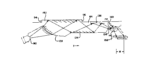
In Fig. 11, the propagation or transfer of the evAnescent wave image is
det~iled in the y-direction, that is, in the direction of the propagation of light, with the
30 optical plate 64 shown in phantom. The source 90 emits radiation in a generally diverging
pattern which is converted to a mildly convergent beam by the aspherical illllmin~ting lens
128. The illuminAting lens 128 spreads the radiant energy from the source across the
platen 130 from its leading edge 94 to its trailing edge 96 so that evAnescent wave image
CA 02203924 1997-04-28
WO 96tl3742 PCTrUS95/14373
14
data presented to the platen 130 can be transferred to the image sensing device 168. By
TIR, the image data is reflected from the platen 130 to the surfaces 134, 136, 138, 140
and through the im~ging lens 142. The image wave converges as it travels toward the
second planar surface 138, and before reaching the second toroidal surface 140, the image
5 wave converges at the nominal focal point FP of the ill~l.l,in~ g lens 128. Thereafter,
the leading and trailing edges of the image wave are inverted, and so the data from the
leading edge 94 of the platen strikes the second toroidal surface 140 at that surface's
trailing edge, and vice versa. The reversed image then exits the optical plate 64 through
the im~ging lens 142 and is transferred to the external image sensing device 168.
In Fig. 12, the same propagation of the evanescent wave image is
illustrated, this time from a front view, that is, showing the x-direction which is transverse
to the direction of the propagation of light in the optical plate 64. As can be seen from
this figure, the ev~n~.scent wave image converges at FP between the second planar surface
138 and the second toroidal surface 140. Prom the views of Figs. 12 and 13, the cone-
15 like convergence of the radiation from the source 90 can be appreciated. Further, the
overall magnification or fan in these directions is preferably configured to be the same.
For example, a construction can be achieved having nearly matching m~gnifi~tions, M,
in the x- and y-axes (Figs. 11 and 12).
In Fig. 13, a second embodiment of the uneven surface detection ~p~dlUS
20 is shown in which features common to the first embodiment are given corresponding
refe~ ce numerals. Otherwise than as specifically described below, this alternative
embodiment shares the inventive lens arrangement adapted to reduce or elimin~te
geometric perspective distortion and ~ctigm~ticm within the optical plate 64, and operates
using the source 90 as described above. However, for certain d~t~bace and security
25 applications, it may be desirable to scan information to supplement finge.~ data, or
simply other information altogether such as bar code or other data. Hence, the optical
system 62' of Fig. 13 includes in addition to the r~lul~s of the optical plate 64, a source
200 mounted on the PCB 66' So as to irradiate the optical plate 64' nearly or subst~nti~lly
normal to the bottom surface 88. In this orientation, the light radiated by the source 200
30 enters the optical plate 64' at A, beneath the p.ese~ tion surface 31, and passes
therethrough to an opposite margin B, at which point it is refracted outward at an angle
somewhat skewed from a line normal to the top surface 86 of the optical plate 64'. The
light irradiated from the source 200-may then impinge upon an object 202 located
CA 02203924 1997-04-28
WO 96/13742 PCT/US95/14373
generally above point B, but not necessarily in contact with or parallel to the presçnt~ti~ n
surface 31. The object 202 may contain a bar code BC or other uneven surface fortran~r~ g to an image sensing device 204 (or image sensing device 168). The image
sensing device 204 may be a linear CCD chip, as commonly used for bar code sç~nning
S in point-of-sale and industrial applications. Allellldli~ely, the image sensing device 168
of the first embo.1imPnt, which is preferably a CCD chip including an image area sensor
(IAR), can be used as a limited-field or linear CCD by prematurely termin~ting the area
scan pattern with a scan reset pulse so that only a few lines in the CCD array are utili7PA.
In this l,lal~el, only that portion of the CCD scan area which receives the transferred
10 image from the object 202 is utilized. In this regard, the complement of other electronic
components 70A,B, ... N mounted on the PCB 66' (not shown in this cross section, but
see Fig. 4) may include circuitry to reset the scan cycle of the image sensing device 168
under control of such circuitry as understood by persons skilled in the art, and may
further include circuitry to switch the mode of operation between that described for the
15 first and second embodiments.
In this embodiment, the optical plate 64' includes a linear prismatic element
206 in the vicinity of the trailing edge 96 of the platen 130. A portion of the light
reflected from the object 202 enters the optical plate 64' through the refractive prismatic
element 206. The light is then reflectively ll~ relled in a manner as previously described
20 to the image sensing device. The linear prismatic element 206 may be integrally formed
on the optical phte 64', and, in any event, is mounted or formed at an angle chosen to
frustrate TIR, in other words, at an angle that is refractively tr~n~mi~ive.
Sc~nning of two--~imP-n~ional bar codes can be facilitated by providing a slot
(not shown) for controlled motion of objects 202 such as credit cards. This slot may be
25 integral to the presentation surface 31, and in particular, can be forrned as part of a
finger-stop or tactile fee~lb~ck means which may also serve as an indicator to the ~ or
of the location of his or her digit 32 on the platen 130.
A fingerprint can be captured at a location remote to the optical plate 64'
for later transfer to the image sensing device by use of a thermally activated sheet of
30 paper. The thermally activated paper responds, for example, to an individual's body
temperature by recording a fingel~fil,l image thereon. The image can then be converted
to a digital format by reflecting the fingel~,finl image data from the thermal paper (which
serves as the object 202 in this exemplary application) using the uneven surface detection
CA 02203924 1997-04-28
WO 96/13742 PCTIIUS95/14373
16
apparatus of Fig. 13.
As a modification of either of the foregoing embo-lim~nt.c, or both, the
resolution pe.fo~ ce can be enhanced by including a device for shulle~ g the external
image sensing device 168, 204 between open and closed positions. Either the evaneccçnt
S wave image from the plese~ ion surface 130 or the bar code data BC from the pri~m~ti~
cl~,llenl 206 is caplul~d when the external image sensing device is shuttered to an open
position. As a result, the object whose image is being transferred (either the digit 32 or
the object 202) iS captured over an abbreviated time period which reduces the exposure
time of the image sensing device and thereby limits the effects of any motion of the object
which might otherwise blur the tMnsferred image. Alternatively or additionally, the
optical system 62' may include a strobing device for intermittently illumin~ting the platen,
and perhaps an actuator for ~ctu~ting the image sensing device and causing same to
capture either evanescent wave or bar code BC image data from the platen 130 or the
prismatic element 206. By pulsing the source intel,-,ill~ntly, the source may be operated
ai a higher level of emission to deliver a nominally equivalent amount of energy in a
shorter period of time without overheating or being damaged. Preferably, the actuator
causes the external image sensing device to capture images in synclhul~ ion with the
intermittent illu~lin~l ions of the platen or prismatic surface. Either the s~ e- ;"~ or the
strobing or both can be accomplished by conventional mechanical or electronic devices.
The surface figure and irregularity of the lenses should be within 20
mnges. In regard to the lens cosmetics, the scratch should be no greater than 60 microns
wide and the dig no greater than 40 microns wide, per surface. The axis of each lens or
molding tool insert should be ground, polished, or both to within 0~1'30". Finally, the
lens centration should be +0.002" on the toroidal surfaces and +0.005" on the other lens
surfaces.
The image sensing device 168 may be a conventional CMOS CCD device.
It is ~refGr,ed that the image area sensor (IAR) be able to resolve 500 dots per inch (DPI).
A conventional CCD chip has 510 X 494 pixels, each of which is (iigiti7~d to an 8 bit
value. 500 DPI is the baseline resolution used by several fingelylilll feature detection
systems, including the Federal Bureau of Investigation's fingel~"i"l identification system
and in a system disclosed in U.S. Application Serial No. 08/036,845 to Shen, filed March
25, 1993, for ME~IOD AND SYSTEM FOR- DETECTING FEATURES OF
FINGERPRINT IN GRAY LEVEL IMAGE, assigned to Cogent Systems, Inc. The
CA 02203924 1997-04-28
W O96/13742 PCTnUS95/14373
17
digiti7~ signal may be filtered to (a) remove background noise, and (b) perform edge
enh~ncement. The edge enh~ncement process sharpens the image and fills in any
erroneous gaps in the ridge of a fingel~flnl. This signal is then ported to a finge~ t
feature detection system such as either of the aforementi~ned systems. This signal is from
5 16K to 40K, depen-ling on the particular application. For example, if the fingel~Jli"
h~fol",alion is tr~ncmitted by hard wire, then a 40K signal can readily be trAncmitted.
However, for efficiency, the digital processor may further include digital compression to
reduce the info"nation down to 16K so that it may be tr~ncmittçd by a wireless link, as
understood by persons skilled in the art. Any acquired fingerprint image data is stored
10 in less than about lK of memory, for example, in a bar code such as by Symbol, in
semiconductor memory (RAM, DRAM, SRAM, EPROM, PROM, ROM), or on optical
or m~gn~tic media (CD ROM, Laserdisk, Mini(lic~, hard disk, or floppy disk), as
understood by those skilled in the art.
In the preferred embodiment, the source 90 emits a small range of
15 wavelen~lhs centered around 565 nm (which appear green to the naked eye), preferably
in the range of 550 to 600 nm. While other wavelen~thc could be used as well, these
preferred wavelengths are selected because they provide a sharp image at the image
sensing device 168 and optimal contrast for flesh-tone fingt;ll,lints. Conventionally, when
the image sensing device is chosen to be a CCD chip, the center wavelength output by the
20 source has been chosen to be at the peak sensitivity of CCD's so that the image sensing
device is made sensitive. This center wavelength is outside of the range of wavelengths
centered about 565 nm. However, because the optical plate 64 efficiently reflects light
to the image sensing device, some sensitivity can be sacrificed in the present design in
favor of image quality, at the discretion of the optical design engin~,er charged with
25 striking a balance between these conflicting design criteria. The reflective surfaces
intermediate the platen 130 and the image sensing device 168 are selected to opli",i~e the
optical design by minimi7ing geometric distortion at the selected source output
wavelength.
While the foregoing IJlerelled embodiment has been described with regard
30 to certain reflective surfaces, other reflective surfaces may be included to create a required
magnifying optical path length in minim~l space. These surfaces may also be TIR and
therefore not require any special reflective coatings, or may be coated to ensure TIR.
As used in this Specification, uneven surface refers to a surface that is
CA 02203924 1997-04-28
Wo 96/13742 Pcrlusssll4373
18
uneven in the physical sense of an irregular surface contour, or uneven in the optical sense
of contrasting surfaces, and in particular, juxtaposed black and white images such as the
bar code BC.
The term "~mge~ " as used in this specification refers to the ridge and
5 groove patterns found on the digits of either hand, including the pinky, ring, middle, and
index fingers as well as the thumb. The term "image processing system" as used herein
refers to the compression, analysis, and matching routines that may be used in conjunction
with the integrated optical system 62 of the present invention. Further, the term "platen"
as used herein embraces the prismatic element 206, notwithstanding any previous
10 ~ c~ssions in which the terms are used in the alternative.
From the foregoing description, it will be clear that the present invention
may be embodied in other specific forms without departing from the spirit or e~ssenti~l
characteristics thereof. Thus, for example, while two embodiments of the uneven surface
image ~ r apparatus have been shown and described, the invention is not limited to
15 these embo-liment~. Other configurations are deemed to be within the scope of the
invention provided they are adapted to m~int~in geometric fidelity as described above.
The ~)lese"lly disclosed embodiments are therefore to be considered in all respects as
illustrative and not restrictive, the scope of the invention being in-~ir~te~ by the appended
claims, and not limited to the foregoing description.