Note: Descriptions are shown in the official language in which they were submitted.
CA 022039~9 1997-04-29
P/60774.CAP/MMS
MULTIPLEXING/DEMULTIPLEXING AN FDM OF RF SIGNAL CHANNELS
This invention relates to " " 11~ /d~ . ""l ~ v an FDM of RF signal channels.
The invention is especially concerned with signal processing on artificial
C.f~ll 1..;. -~;11.1~ satellites, and particularly output "il ' _
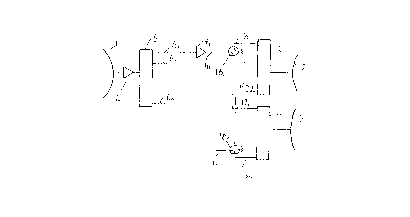
Referring to Figure 1, a typical on-board system comprises a receiving antenna I and two
l~ e antennas 2, 3. The ~l v antennas may point to different regions of
the earth. The uplink signal received by the receiving antenna will be an FDM (Figure
2) of n channels of a certain bandwidth and, after ~ by low noise amplifier
10 4, 'i ~ll;llr rl 5 separates the signal into n channels 6,-6n (usually equispaced
frequency slots) which are ' v ' '1~ amplified by amplifiers such as travelling wave
tubes 71-7n These signals are then switched between output ~ lLi"l~ 8, 9 feeding
the antemnas 2, 3, by means of switches 16,'16n, which are commected to the travelling
wave tube amplifiers 71-7n on the one hand and to the output 1 ~ 8, 9 on the
other hand by individual waveguide sections 111-l ln and 121-12n, 131-13n
Referring to Figure 3, which shows the circuit of the output multiplexer 8, the signal
channels are mllltirll~Yrd by launching ~Iv.,~lUI~ Lic radiation from each waveguide
121-12n into a waveguide manifold 13, short circuited at the end 13a at a respective
20 precise distance from the short circuited end which is related to the wavelength, in order
to produce standing waves in the waveguide 13. Each chamnel is filtered via a respective
two-port filter 14,-14n The problem with such a design is that the filters have to be
CA 022039~9 1997-04-29
2 P/60774.CAP/MMS
tuned in situ because the tuning of each filter affects the tuning of the others.
In order to overcome this, as well as to reduce the weight of the satellite, the use of
directional filters (Figure 4, 5) has been proposed. With this ,.,,,..~c,..,. - each
5 travelling wave tube amplifier 71-7n can be alternately comnected to one of two ports on
a single output multiplexer 15 by means of respective switches 161-16n. In the first
switch positio4 the signals enter the directional filter by one input port a, producing
travelling waves ylu~ i;..,., along the waveguide 18 of the output multiplexer 15, as
shown in Figure 5, in a right hand direction to feed the antenna 2, while the left hand
lû side of the waveguide 18 is terminated by the second antenna 3. In the other switch
positio4 the signals enter the directional filters by means of the other input port b,
producing travelling waves ,UlUya~ lg along the waveguide 18 of the output
AGI 15 in the opposite direction to feed the second antenna 3, while the right
hand side of the waveguide 18 is still terminated by the first antemna 2.
Figure 6 shows the pass-band response of the filters when signals are fed in at port a for
feeding antenna 2. The filter pass-bands are contiguous. The pass-band response (firom
a to d, and b to c) and band stop response (firom a to b, and c to d) of one of the filters 17
(shown in Figure 7a) are shown in more detail in Figures 7b and 7c, ..,",~ . The
20 pass-band response of the filters is the same when signals are fed in at port b for feeding
antenna 3.
In the interests of maximising traffic carried by the on-board satellite signal processing
system, each channel is defined by a band pass filter with steeply descending transition
CA 022039~9 1997-04-29
3 P/60774.CAP/MMS
regions in order to allow closely spaced narrow bands. In order to achieve this,
directional fikers employing a succession of cavities with more than one resonance per
cavity has been disclosed (BP 0 249 612 B) with a quasi-elliptic response. However, it
is a ~ ' ' law that for mirlimum phase networks the narrower the bandwidth, the
5 greater the variation of group delay across that bandwidth.
The invention provides a multiplexer for producing an FDM of RF signal channels,
comprising a l, ~ Iine, a plurality of directional filters by means of which
respective signals can be coupled onto the L.a~.D.~ . line, wherein at least one of the
10 channels of the resulting FDM on the ll~l~ll..~D;OI~ line is defined at one edge by the
band pass response of the directional filter coupling the respective signal onto the
~. line and at the other edge by the band stop response of another directional
filter for coupling another signal onto the ll~ilDll.i~.;ol~ line.
15 The pass band response of each directional filter may now be greater than the signal
channel, permitting a reduced variation of group delay across the bandwidth.
The directional filters may be . ' ~ as cavity resonators. An input and output
dual-mode cavity resonator may be used to provide separate coupling paths into and out
20 of a pair of ~uallu~Jlc mode cavities which contain all the necessary mutual and cross-
couplings to produce a desired elliptic response via lon~it~ coupling slots only.
Multiplexers constructed in accordance with the invention will now be described, by way
of example, with reference to the acc~ , drawings, in which
CA 022039~9 1997-04-29
4 P/60774 CAP/MMS
Figure I illustrates a known satellite on-board repeater including two output
Figure 2 illustrates ' "~, a frequency division multiplex;
Figure 3 shows the circuit of the output ~ of Figure l;
Figure 4 shows a known satellite on-board repeater including a single directional output
"",llil~l. . .-"
Figure 5 shows the circuit of the directional output multiplexer of Figure 4;
Figure 6 shows the ~u~ DtOIlJill~ pass-bands of the directional filters of the output
multiplexer of Figure 5;
Figure 7a shows one of the &rectional filters of Figure 5 in more detail;
Figure 7b shows the filter pass-band response from port a to d, and b to c, and vice versa;
20 Figure 7c shows the filter band stop response from port a to b, and from port c to d, and
vice versa;
Figure 8 shows the circuit of an output multiplexer in accordance with the invention;
CA 022039~9 1997-04-29
5 P/60774.CAP/MMS
Figure 9a shows the pass-band response of the directional filters of the output
multiplexer of Figure 8 from port a to d, or port b to c;
Figure 9b shows the band-stop response of the directional filters of the output
5 multiplexer of Figure 8 from port c to d or vice versa;
Figure 9c shows the ~,o.l.,~,o..l;..g channels of the FDM multiplex produced by the
output multiplexer of Figure 8;
10 Figure 10 is a perspective view of one form of directional filter suitable for use in the
output multiplexer of Figure 8;
Figure 11 shows one of the cavities of the directional filter shown in Figure 10;
15 Figure 12 shows the pass-band and stop-band response cu--~ u~ to various ports
of the directional filter; and
Figure 13 shows the overall response resulting from the two responses shown in Figure
12.
Throughout all the drawings, like reference numerals have been given to like parts.
The satellite on-board processing system which includes the output multiplexer is as
shown in Figure 4 of the drawings. The output multiplexer (Figure 8) consists of a
CA 022039~9 1997-04-29
6 P/60774.CAP/MMS
all~laa;ull line in the form of a waveguide 18 commected to transmit antenna 2 at one
end and a transmit antenna 3 at the other end. The multiplexer also includes n
directional filters 171-7n, which are supplied via switches 16-16 w4ich in turn are
comnected by waveguide to respective travelling wave tube amplifiers 71~7n which output
5 the channels d , ~ from the (~ l- ~, 5 of Figure 4. It is assumed that
only chamnels I -n are connected, chalmels I '-n ' will be referred to hereinafter.
In accordance with the invention, the filtering operation for each channel (apart from the
nth filter when antenna 2 is used and the first filter when antenna 3 is used) is performed
10 by two directional filters and not one as hitherto. Thus, the pass-band of directional filter
171 from terminal a to terminal d (Figure 9a) is ~IJplU~lla~ twice the desired width
of the signal channel I (Figure 9c), so that the signal passing along the waveguide 18
towards directional filter 172 actually overlaps signal chalmel 2. However, the frequency
response of directional filter 172 between terminals c and d is a band-stop response
15 (Figures 7c and 9b). The lower frequency transition of the first channel I (Figure 9c) is
thus defined by the lower frequency transition of the pass-band of the first filter 171 ~
whereas the higher frequency transition of the first chalmel I is defined by the lower
frequency transition of the band stop response of the second filter 172.
20 Because the pass-bands and stop bands of the filters are greater than hitherto, group
delay is reduced, which means that there is reduced amplitude variation.
Each directional filter has a pass-band from a-d (or from b-c), and a band stop response
CA 02203959 1997-04-29
7 P/60774.CAP/MMS
from c-d or d-c with the same transition regions. The difference from the pnor alt
of Figures 5 and 6 is that each pass-band/band stop region is wider in
relation to the channel than hitherto (in this case, twice as wide), and adjacent pass-
band/band stop regions overlap each other.
The second channel 2 is defined in the same way as for the first channel, ie. by
directional filters 172 (lower frequency edge) and by directional filters 17 (l~igher
frequency edge). It will be observed that the last charmel n will therefore be twice as
wide as the other channels, since there is no adjacent band stop.
The resulting FDM (Figure 9c) is fed to antenna 2 for
It will also be observed that the configuration of Figure 8 also lends itself to Ll
to antenna3. Inthiscase,inputsl'ton'oftheswitchesl6,tol6nareusedinplaceof
15 inputs l-n. In this case, the first channel will be oftwice the normal width, and the last
channel n will be of normal width. Thus, filter 17" receives input I ', which passes into
port b and out of port c. This will define the higher frequency transition of the channel
n. The lower frequency transition will be defined by the upper frequency transition of
the band-stop of filter 17n l. The other channels will be defined in the same way, except
20 for channel I (derived from input 2 ' and directional filter 172 ), which will be of twice
the width of the other channels since there is no succeeding band stop. This time the
FDM is launched from antenna 3.
CA 022039~9 1997-04-29
8 P/60774.CAP/~fMS
In fact, while the n ' inputs produce n channels, in fact they do not occupy the frequency
slots of their Cuu~ the inputs n. Thus, to take filter 172 as an example, when the
inputs n are present, its output (from input 2) falls in channel slot 2 (pass-band of 172 and
band stop of 173), whereas when the inputs n' are present, its input (actually 3 ' ) now
leaves port c and occupies channel slot 3 (pass-band of 172 but band stop of 17, ).
It follows that each directional filter can be fed with two different channel slots
'~" and both antennas 2, 3 can be used ! ~ , each using the same
set offrequency slots (apart from the differences at the ends noted above). Provided the
10 antennas are &rected at different regions of the earth, twice as many signals can be
broadcast as with the prior C.UII~;UI ~;UII of Figure 5, for the same number of filters and
the same number of switches. (It would not be possible to feed both inputs of each filter
of Figure 5 with signals occupying the same frequency slot to achieve the same result
because there would be ~ C~ Ir crosstalk between the signals in the filters).
A practical .~ of the &rectional filter 17 is shown in Figures 10 and 11.
Figure 10 shows the general a". ,,~.,....l of the four-port directional filter when
;,..j.l .,...,(td using multimode cavity resonators. The inputs a, b are connected to
respective switches 16" 162 etc, and the outputs c, d are joined to the outputs c, d of the
next adjacent directional filters by extensions of the waveguide i.e. the output waveguide
18 is a continuous length of waveguide which includes a section c-d as shown in Figure
10 for each directional filter.
CA 022039~9 1997-04-29
9 P/60774.CAP/MMS
The directional filter is formed by an input waveguide 22 and a parallel waveguide 21
which are ;llt~ e-' by cylindrical cavity resonators 27 and 28 so that two distinct
paths co-exist. The paths illustrated in the figure are, Srstly, from input dual-mode
resonator 27, coupled to the input waveguide 22, to quadruple-mode resonator 28,5 located on the output waveguide 21, then through to output dual-mode resonator 27,
coupled to the output waveguide 21; secondly, input dual mode-resonator 27, coupled
to the input waveguide 22, then to quadruple-mode resonator 28, located on the input
waveguide 22, then to output dual-mode resonator 27, coupled to the output waveguide
21.
Other than the routing, the two paths should have identical electrical .,I~ L~;.;a~;.,a
particularly in respect of signal phase shift and group delay. Physically, the ~ L
illustrated is not a definitive ~IllI,o.l;lll.,.lL, in terms of relative sizes and/or aspect ratio,
but typifies the ' ~ of a separate input and output waveguide with means
15 which create two distinct filter paths each using at least one ~u~d~u~l~, mode cavity
coupled only with l.~ . ' slots.
In the particular ~ o~ of the invention illustrated in Figure 10, cavity resonators
27 and 28 are of the form of right circular cylinders closed off at both ends. The input
20 and output waveguides 22 and 21 are cu..~.,..i;u.~l rectangular conducting tubes suitably
~' I so as to allow el~LIu~.a~ ,L;c p-up~...;ûll in the dominant TElo waveguide
mode. The input waveguide 22 has a pair of opposing ends a and b which serve as
inputs of the directional filter and are used depending on the required signal flow
direction through the filter. Similarly, the output waveguide 21 has a pair of opposing
CA 022039~9 1997-04-29
10 P/60774.CAP/~IS
ends c and d which serve as outputs from the directional filter depending on the required
signal flow direction through the filter
In operation, an elf,~ u~ ic wave, whose frequency falls in the pass-band of the
5 filter, is input to one of the ends a, b of the input waveguide 22 and the filtered wave
emerges from one of the opposing ends c, d of the output waveguide 21. Alternatively,
when an el~c~ ~ wave, whose frequency does not fall in the pass-band of the
filter, is input to one of the opposing ends of the input waveguide, it emerges only from
the opposite end of the input waveguide to which it was input and so is passed on,
10 unaffected, as an input to another such filter. Like the output waveguide, the irlput
waveguide ls also a, of the waveguide sections a, b.
A number of such filters are ill~eluu~ cd and both the input or output ~ U;~cl~
form a travelling wave manifold. This is illustrated in Figure 8 ICIJII " ,, an output
1 5 multiplexer.
The circular dual-mode cavity resonators 27 are ~ ' so as to support a TEIll
circularly polarised waveguide mode. Coupling into the input cavity 27, from the input
I cc~all~uku waveg ude 22, and out of the output cavity 27, into the output rectangular
20 waveguide 21, is via an aperture suitably located to couple equal amounts of energy from
the longitudinal and transverse f. ", ~ of the rectangular ~vc~;uid~,., TEIo dûminant
mode. This coupling aperture may be a simple circular hole 30 or another more complex
aperture structure, as long as the resulting coupled ~ in the circular cavity
resonator have a quadrature relationship in both time and space.
CA 022039~9 l997-04-29
I I P/60774.CAP/MMS
A pair of lc.n~itl~ ' ' coupling slots 29, located in the cylindrical wall of input cavity
resonator 27 and energised by the magnetic field of the ele~,~lUllla~ ,;iC, wave therein,
have an orthogonal relationship so that the TE", circular polarisation is dcr,o..l~.o~e~ into
two coupling signals which are in phase quadrature. These signals are the means of
5 providing separate paths through the filter each being coupled into one of two quadruple-
mode cavity resonators 28 the outputs of which are similarly coupled, by similar
l,~ngitllllin~ slots 29, to the output cavity resonator 27 where the two signals are again
recombined into a TEI,l circularly polarised wave. This wave is finally coupled into the
output rectangular waveguide via a coupling aperture 30 which may be a simple circular
10 hole or another more complex aperture structure.
The mode c.."l~ , of the two quadruple-mode cavity resonators is illustrated in
Figure l l which shows arrows numbered 1-4 indicating the electric vectors of the four
;...1~,",..~. ..1 linearly polarised and orthogonal waves therein. The cavity must be
15 suitably l; ... - - ...~ 1 so that it will support a pair of orthogonal TEl~N modes and a pair
of orthogonal TMllo modes. Here, N can be any convenient integer value. Also shown
is the mput and output l. ~,i~ ' ' slots 29, and 292 ~~ ,.,Li~,ly, o. i' ~ disposed
and located in the cylindrical cavity wall, together with four additional couplings 3 7, 3 8,
39 and 40 formed by simple capacitive posts, or screws. O~,w~;o "~, the magnetic field
20 coupled from slot 29, will couple into the first TE,IN mode-l. Inclusion of coupling
post, or screw, 38, at 45 ~ to a common plane and at the intersection of the cylindrical
wall and the cavities closed end, will further excite the first TMllo mode-2. Inclusion of
the post, or screw, 37 suitably positioned in the closed end of the cylindrical cavity, will
energise the second TMllo mode-3 . Finally, the inclusion of the coupling post, or screw,
CA 022039~9 1997-04-29
12 P/60774.CAP/MMS
39, at 45~ to a common plane and at the intersection of the cylindrical wall and the
closed end ofthe cavity, will couple into the second, and last, TEIIN mode-4. The energy
of this fourth mode is coupled out of the cavity via the second l- n~it--~lin~l slot 292
excited by the magnetic field of this mode. The addition of coupling post, or screw, 40
5 forms a cross-coupling between the first and fourth TE"N modes so that a a~ ;.,al
pair of finite frequency ~1 allal~fi.a;ull zeros is produced.
In the general ~u. " t, shown in Figure 10, additional capacitive posts, or screws,
31, 32, 33, 34, 35 and 36 are provided to ensure that each mode is tuned to the same
10 resonant frequency enabling a~ ,LIl to be achieved through each of the two filter
paths. Each separate filter path, from input waveguide 22 to output waveguide 21,
therefore makes use of at least one I ~ ' 1, or transverse, resonance in the first dual-
mode cavity 27, two TE and two TM modes in one of the quadruple-mode cavities 28,
and one transverse, or 1( ,, ' 1, resonance in the second dual-mode cavity 27. A
15 symmetric pair of finite frequency 1- zeros is ~ produced by the
cross-coupling post, or screw, 40 in the 4Ua~l u~ -mode cavity 28. Therefore, each path
provides for at least six ~.. poles together with a symmetric pair of finite
frequency zeros, known as a quasi-elliptic ~la~ a~;UII function, without the need for
a cross-coupling via a separate cross-coupling aperture or slot.
As has been previously described, it is desirable that, in a travelling wave manifold
dl I all~ , the individual directional filter pass-bands overlap. This technique can be
more easily understood by considering an output multiplexer, using four-port directional
filters, as d;a~ "~, represented in Figure 8 where all inputs b are terminated with
CA 02203959 1997-04-29
13 P/60774.CAP/MMS
refic-ction-less loads and signal inputs into a, at frequency fr, are directed to output d on
the manifold.
The llallallG~a;ull function for filter 17~, from al to d" may be represented by the quasi-
5 elliptical band-pass response as indicated by trace A in Figure 12. Due to the presence
ofthe re'dection-less termination port b of directional filter 172, the ~-; function
from c to d at directional filter 172, assuming a similar q..~ 'li, ' band-pass response
for 172 as for 17, except for a .1: ,"li~_.. - in pass-band centre frequency, will
be that known as a band stop response typified by trace B in Figure 12. If the overlap
10 in responses is equat to a~ halfthe ~- bandwidth then the overall
I l hl l~ response from input a of 17, to d of 172 will be the product of A and B as
shown in Figure 13 . Note that the new pass-band width is ~~ , half that of the
original filter, the stop band response zeros of filter 172 have become i zeros
in the overall response of filter 17~, and the high frequency roll-off region is entirely
15 defined by the stop band . I -- i.. ~ rl ;'l ;~. of the next adjacent dGrectional filter.
It is found that a band-pass ll response so produced provides for a number of
advantages over c~ ;ul.al methods of channel definition, in terms of
of signal fideGty provided by the i path from any input to the common output
20 ofthe ~llfirl~Y~r, in as much as for the same shape factor, or selectivity, reduced pass-
band amplitude and group delay variation is obtained.
This process of pass-band definition by uv~lla}~ pass-bands described is extendible
to include as many channels as is deemed necessary to make a functioning frequency
CA 022039~9 1997-04-29
14 P/60774.CAP/MMS
division power combining manifold.
The reciprocal nature of the technique also provides for an exactly similar process when
the manifold is used in the reverse direction so as to provide a firequency division de-
5 multiplexer. This, in Figure 8, anteMa 3 could be a receive anteMa providing an FDMsignal which, after low-noise ~rlifir~ti~n, would be fed along waveguide 1~ and
divided mto respective signal chaMels l-n. In tbis example, chaMel I would be defined
by the full pass-band width of directional filter 171, with signal energy entering port c
and emerging firom port b and thence firom port 2' of switch 162 . Channel 2 would be
10 defined by the part of the pass-band response of directional filter 172 which does not
coincide with the band-stop response, from port c to d, of directional filter 171 . Thus,
for filters the centres of wbich increase with firequency in ordmal sequence, channel 2
is defined by the lower firequency ~UIIU~JO~ to the upper stop-band edge of
directional filter 171, and the upper firequency Cull~ " " to the upper pass-band of
15 directional filter 172. Therefore, received signals whose firequency CU~ Oil~,...~ fall
between these two limits are unaffected by the band-stop response of directional filter
171, and so enter port c to emerge from port b of directional filter 172 and thence firom
port 3' of switch 163.
20 If anteMa 2 receives the FDM of signals, the chaMels are similarly divided into
respective channels n-l but emerge firom ports a and thence from the ports l-n of
switches 16n - 161. In this case chaMel n is defined by the full pass-band width of
directional filter 17n whilst the remaining channels become defined as described
previously
CA 022039~9 1997-04-29
15 P/60774 CAP/MMS
The invention is not restricted to directional filter illustrated in Fig. 10. Thus, the
directional filter described inEP 0 249 612B could be used, or other types could be used.
Typical frequencies of operation are microwave eg. 30MHz to 300GHz.
It is not necessary for each channel to represent one signal only Two signals could be
contained in one channel or, more generally, the channel could be digital, for example,
time division ~ 1 data.
10 Also, it is not necessary for the filters to be physically positioned in the order of the
channels they define. They could be physically positioned irl any order, and the channels
will be unaffected.