Note: Descriptions are shown in the official language in which they were submitted.
CA 02204046 1998-09-10
DIFFERENTIAL DETECTION DEMODULATOR AND PHASE COMPARATOR
THEREFOR
This invention relates to differential detection
demodulators used in the radio communication systems, and
more particularly to improvements in frequency converter and
the phase comparator or the phase detection circuit used in
differential detection demodulators. This application is
divided from co-pending Canadian Patent Application Serial
Number 2,086,279 filed December 24, 1992.
A conventional differential detection demodulator
provided with a frequency converter and a phase comparator
is disclosed, for example, in Japanese Laid-Open Patent
(Kokai) No. 64-12646, "DPSK demodulation system". The above
conventional differential detection demodulator which will
be described in greater detail later, has the following
disadvantages. Since the frequency converter and the phase
comparator circuits are composed of analog components,
integration of circuit parts into ICs is difficult. Thus,
the adjustment or tuning of circuits is problematic.
Further, it is difficult to reduce the size and the power
consumption of the circuit.
This invention provides a differential detection
demodulator provided with a frequency converter and a phase
- 1 -
CA 02204046 1998-09-10
comparator consisting of digital circuit elements, such that
the circuit can easily be integrated into ICs and hence the
adjustment step of the circuits can be dispensed with and
the size and the power consumption can be reduced.
In accordance with the present invention there is
provided a phase comparator for determining a phase shift of
a 2-level received signal relative to a phase reference
signal having a fixed frequency practically equal to a
frequency of the received signal, the phase comparator
comprising: an exclusive OR element for obtaining a logical
exclusive OR of the received signal and the phase reference
signal; absolute phase shift measurement means coupled to
the exclusive OR element, for determining a duration in
which an output of the exclusive OR element is sustained at
a logical "1" during each half period of the phase reference
signal; and phase shift polarity decision means coupled to
the exclusive OR element, for decision whether the phase of
the received signal is lagged or led with reference to the
phase reference signal, on the basis of a value of the
exclusive OR element at each half period of the phase
reference signal; wherein a combination of outputs of the
absolute phase shift measurement means and the phase shift
polarity decision means represents the phase shift of the
received signal relative to the phase reference signal.
- 2 -
CA 02204046 1998-09-10
Preferably, the absolute phase shift measurement means
comprises: an adder coupled to the exclusive OR element; and
a delay element having an input coupled to an output of the
adder and having an output coupled to an input of the adder,
the delay element delaying the output of the adder in
synchronism with a clock having a period shorter than the
period of the phase reference signal, the_delay element being
reset at each half period of the phase reference signal
wherein the adder adds outputs of the exclusive OR element
and the delay element to obtain a value corresponding to the
duration in which the output of the exclusive OR element is
sustained at a logical "1" during each half period of the
phase reference signal.
The differential detection demodulator according to this
invention for demodulating a 2-level received signal using a
phase reference signal having a fixed frequency practically
equal to a frequency of the received signal, the differential
detection demodulator comprises: a phase comparator
including: an exclusive OR element for obtaining a logical
exclusive OR of the received signal and the phase reference
signal; absolute phase shift measurement means coupled to the
exclusive OR element, for measuring a duration in which an
output of the exclusive OR element is sustained at a logical
"1" during each half period of the phase reference signal:
and phase shift polarity decision means coupled to the
exclusive OR element, for decision whether the phase of the
received signal is lagged or led with reference to the phase
reference signal, on the basis of a output value of the
exclusive OR element at each half period of the phase
reference signal; wherein a combination of outputs of the _ _
absolute phase shift measurement means and the phase shift
polarity decision means constituting a relative phase signal
output from the phase comparator: a delay element coupled to
the phase comparator, for delaying the relative phase signal
output from the phase comparator by one symbol period of -the
received signal: and a subtractor coupled to the phase -
- 3 -
CA 02204046 1998-09-10
comparator and the delay element, for subtracting an output
of the delay element from the relative phase signal.
Alternatively, the differential detection demodulator
according to this invention for demodulating a first 2-level
signal using a phase reference signal having a fixed
frequency practically equal to a frequency of the first
signal, the differential detection demodulator comprises: a
frequency converter circuit for converting the frequency of
the first signal using a second 2-level signal having a
frequency distinct from the frequency of the first signal,
including: an exclusive OR element for obtaining a logical
exclusive OR of the first and second signal; running average
generator means, coupled to the exclusive OR element, for
generating a signal corresponding to k times running average
of an output of the exclusive OR element, k being a positive
integer; and hard decision means, coupled to the running
average generator means, for converting an output of the
running average generator means to a 2-level logical signal,
an output of the hard decision means constituting an output
of the frequency converter: a phase comparator including: an
exclusive OR element coupled to the hard decision means of
the frequency converter, for obtaining a logical exclusive OR
of the output the frequency converter and the phase reference
signal: absolute phase shift measurement means coupled to the
exclusive OR element, for measuring a duration in which an
output of the exclusive OR element is sustained at a logical
"1" during each half period of the phase reference signal:
and phase shift polarity decision means coupled to the
exclusive OR element, for decision whether the phase of-the
first signal is lagged or led with reference to the phase
reference signal, on the basis of a output value of the
exclusive OR element at each half period of the phase
reference signal: wherein a combination of outputs of the
absolute phase shift measurement means and the phase shift
polarity decision means constituting a relative phase signal
output from the phase comparator; a delay element coupled to
- 4, - _
CA 02204046 1998-09-10
the phase comparator, for delaying the relative phase signal
output from the phase comparator by one symbol period of the
first signal; and a subtractor coupled to the phase
comparator and the delay element for subtracting an output
of the delay element from the relative phase signal.
Aspects of the prior art and present invention will be
described by reference to the accompanying drawings, in
which:
Fig. 1 is a block diagram showing the circuit structure
of a differential detection demodulator provided with a
frequency converter and a phase comparator according to this
invention;
Fig. 2 is a timing chart showing waveforms within the
frequency converter in the case where the shift register has
five stages to hold respective bits;
Fig. 3 is a timing chart showing the waveforms of the
phase reference signal, the received signal after the
frequency conversion, and the output of the exclusive OR
element 61 of Fig. 1, in the two cases where the received
signal after frequency conversion is leading, hereinafter
referred to as led, (shown above) and lagging, known
hereafter as lagged (shown below) with respect to the phase
reference signal;
- 5 -
CA 02204046 1998-09-10
Fig. 4 is a timing chart showing the waveforms
occurring within the absolute phase shift measurement means
62 of Fig. 1 when the received signal after the frequency
conversion is led relative to the phase reference signal, in
the case where the clock frequency of the D flip-flop array
64 is 16 times the frequency of the phase reference signal;
Fig. 5 is a timing chart showing the same waveforms as
those of Fig. 4, occurring when the received signal after
the frequency conversion is lagged relative to the phase
reference signal;
Fig. 6 is a timing chart showing the waveforms related
to the operation of the D flip-flop 66 of Fig. 1;
- 6 -
CA 02204046 1998-09-10
Fig. 7 is a block diagram showing the circuit structure
of another differential detection demodulator according to
this invention;
Fig. 8 is a block diagram showing a conventional
differential detection demodulator provided with a frequency
converter and a phase comparator;
Fig. 9 is a block diagram showing the structure of a
conventional digital differential detection demodulator
provided with a phase detection circuit;
l0 Fig. l0 is a timing chart showing waveforms exemplifying
the operation of a phase detection circuit of Fig. 9 in the
case where the relative phase of the received signal with
respect to the virtual phase reference signal remains
constant;
Fig. 11 is a timing chart showing waveforms exemplifying
the operation of a phase detection circuit of Fig. 9, in the
case where the relative phase of the received signal with
respect to the virtual phase reference signal varies:
Fig. 12 is a block diagram of a differential detection
20 demodulator provided With a phase detection circuit according
to this invention, by which the value of the relative phase
of the 2-level quantized received signal with respect to the
virtual phase reference signal can be updated two times for
each period of the 2-level quantized received signal;
Fig. 13 is a timing chart showing waveforms exemplifying
the operation of the delay element 401 and the exclusive OR
element 402 of Fig. 12;
Fig. 14 is a timing chart exemplifying the waveforms of
the output of the modulo 2N counter 403, the virtual phase
- 30 reference signal, the 2-level quantized received signal, and
the differential pulse signal of Fig. 12, in the case where N
_ 8:
Fig. 15 is a timing chart showing the waveforms
exemplifying the operation of the phase detection circuit_400
of Fig. 12, where N = 8 (2N = 16) and where the relative
_ - 7 _ _
CA 02204046 1998-09-10
phase of the 2-level quantized received signal with respect
to the virtual phase reference signal remains constant:
Fig. 16 is a view similar to that of Fig. 15, but
showing the case where the relative phase of the 2-level
quantized received~signal with respect to the virtual phase
reference signal is increasingly lagged:
Fig. 17 is a view simi~.ar to that of Fig. 15, but
showing the case where the relative phase of the two-value
quantized received signal with respect to the virtual phase
reference signal is increasingly lead:
Fig. 18 is a block diagram of another differential
detection demodulator provided with a phase detection circuit
according to this invention, by which the value of the
relative phase of the 2-level qnantized received signal with
respect to the virtual phase reference signal can be updated
two times for each period of the 2-level quantized received
signal;
Fig. 19 is a timing chart showing the waveforms
exemplifying the operation of the phase detection circuit
400a of Fig. 18, where M = 4 (2M = 16), and where the relative
phase of the 2-level quantized received signal with respect
to the virtual phase reference signal remains constant;
Fig. 20 is a view similar to that of Fig. 19, but
showing the case where the relative phase of the 2-level
quantized received signal with respect to the virtual phase
reference signal is increasingly lagged;
Fig. 21 is a view similar to that of Fig. 19, but
showing the case where the relative phase of the 2-level
quantized received signal with respect to the virtual phase
reference signal in increasingly led; - -
Fig. 22 recapitulates the frequency converter 20 of Fig.
8: and
Fig. 23 is a block diagram showing an alternate
structure of the frequency converter according to this
invention.
_ g _
CA 02204046 1998-09-10
In the drawings, like reference numerals represent like
or corresponding parts or portions.
In Fig. 8, the frequency converter 20 includes a
multiplier 21 and a low pass filter 22. The phase comparator
30 includes: a phase shifter 31 for shifting the phase of
the local carrier (the phase reference signal) by ~r/2
radians; a multiplier 32 for multiplying the local carrier by
the output of the low pass filter 22: a multiplier 33 for
multiplying the output of the phase shifter 31 by that of the
low pass filter 22~: a low pass filter 34 for eliminating the
high frequency components from the output of the multiplier
32; a low pass filter.35 for eliminating the high frequency
components from the output of the multiplier 33; a sampler 36
for sampling the output of the low pass filter 34: a sampler
37 for sampling the output of the low pass filter 35: and a
coordinate converter 38 for calculating and generating a
relative phase signal from the outputs of the~samplers 36 and
37. A delay element 40 delays the relative phase signal by
one symbol period of the received signal. A subtractor 41
subtracts, in modulo 2~, the relative phase signal delayed by
one symbol period by the delay element 40 from the relative
phase signal directly output from the coordinate converter
38. A decision circuit 42 outputs the demodulated data
according to the values of phase_tr_ansition over each symbol
period of the received signal.
Next the operation of the circuit of Fig. 8 is described
in detail. It is a common practice in the field of
demodulators to convert the frequencies of the received
signal to low frequencies using a frequency converter. This
facilitates subsequent signal processing. The received
- 9 -
CA 02204046 1998-09-10
signal is a differential phase shift keying (DPSK) signal.
This received signal is input to the frequency converter 20,
where the multiplier 21 multiplies it by the signal for
frequency conversion. It is assumed that the frequency of
the received signal is fl Hz and that of the frequency
conversion signal f2 Hz. Then the multiplied signal output
from the multiplier 21 includes a high frequency component at
fl + f2 Hz and a low frequency component at ~~ fl - f2 , Hz.
This multiplied signal output from the multiplier 21 is
supplied to the low pass filter 22, where the high frequency
component is suppressed and only the low frequency component
at ~ fl - f2 ~ Hz is passed. The received signal thus
undergoes the frequency conversion.
After being subjected to the frequency conversion by the
frequency converter 20, the received signal is processed by
the phase comparator 30. The multiplier 32 multiplies the
received signal after. the frequency conversion (output from
the frequency converter 20) by the phase reference signal
(the local carrier). The low pass filter 34 eliminates the
high frequency components from the output of the multiplier
32, thereby obtaining the base band signal in phase with the
local carrier (referred to as the in-phase base band signal).
The phase shifter 31 shifts the phase of the phase
reference signal or the local carrier by ~r/2 radians. The
multiplier 33 multiplies the received signal after the -
frequency conversion (output from the frequency converter 20)
by the output of the phase shifter 31. The low pass filter 35
eliminates the high frequency components from the output of
the multiplier 33, thereby obtaining the base band signal in
quadrature w~.th_the local carrier (referred to as the
quadrature base band signal).
The in-phase base band signal output from the low pass
filter 34 is sampled by the sampler 36 and supplied to the
coordinate converter 38. Similarly, the quadrature base band
signal output from the low pass filter 35 is sampled by the
sampler 37 and supplied to the coordinate converter 38. The
-10-
CA 02204046 1998-09-10
coordinate converter 38 outputs the relative phase signal
representing the phase shift of the received signal after
frequency conversion relative to the local carrier, i.e. the
phase reference signal. The value of the relative phase
signal 8 is expressed by the values x and y of the sampled
in-phase and quadrature base band signals as follows:
- a = tan-1 (x/y)
The relative phase signal output from the coordinate
converter 38 is supplied to the subtractor 41 and the delay
element 40. At the delay element 40 the relative phase
signal is delayed by one symbol period of the received signal
and then is supplied to the subtractor 41. The subtractor 41
subtracts, in modulo 2R, the output of the delay element 40
from the output of the coordinate converter 38, and thereby
obtains the phase shift difference signal (abbreviated
hereinafter to phase difference signal).
The phase difference signal output from the subtractor
41 represents the phase transition over each symbol period of
the received signal. Upon receiving the phase difference
signal from the subtractor 41, the decision circuit 42
obtains the demodulated data on the basis of the
predetermined correspondence relationship between the phase
difference signal and the demodulated data.
._ 3 9
-11 -
CA 02204046 1998-09-10
Referring now to the accompanying drawings, the
preferred embodiments of this invention are described.
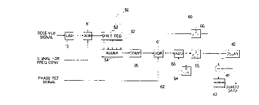
Fig. 1 is a block diagram showing the circuit structure
of a differential detection demodulator provided with a
frequency converter and a phase comparator according to this
invention. A limiter amplifier 10 subjects the received
signal to a 2-level quantization. A frequency converter 50
coupled to the limiter amplifier 10 effects a frequency
conversion on the 2-level quantized received signal output
from the limiter amplifier 10. The frequency converter 50 is
organized as follows. An exclusive OR element 51 is coupled
to the limiter amplifier 10 to obtain the logical exclusive
OR of the output of the limiter amplifier 10 and the signal
for frequency conversion (the frequency conversion signal).
A running average generator 52 removes the high frequency
-12
CA 02204046 1998-09-10
components from the output of the exclusive OR element 51.
The running average generator 52 includes: a shift register
53 for sequentially delaying the output of the exclusive OR
element 51: and an adder 54 for adding the output bits of the
shift register 53. A comparator 55 coupled to the adder 54
compares the output of the adder 54 with a predetermined
threshold value. _ _
Further, a phase comparator 60 is coupled to the
frequency.converter 50 to compare the phase of output of the
frequency converter 50 (the received signal after frequency
conversion) and the phase of the phase reference signal. The
phase comparator 60 is organized as follows. An exclusive OR
element 61 coupled, to the comparator 55 effects the logical
exclusive OR operation upon the output of the comparator 55
and the phase reference signal. In response to the output of
the exclusive OR element 61, an absolute phase shift
measurement means 62 determines the absolute value of the
phase shift of the received signal after frequency conversion
relative to the phase reference signal. The absolute phase
shift measurement means 62 includes an adder 63 coupled to
the exclusive OR element 61 and a pair of D flip-flops 64 and
65 coupled to the adder 63. The output of the D flip-flop
array 64, delaying the output of the adder 63, is returned to
the adder 63. The adder 63 adds the outputs of the exclusive
OR element 61 and the D flip-flop array 64. The D flip-flop
array 65 stores the output of the adder 63. The phase
comparator 60 further includes a D flip-flop 66. In response
to the output of the exclusive OR element 61, the D flip-flop
66 decides whether the phase of the received signal after
frequency conversion is led or lagged relative to the phase
reference signal. The bits output from the D flip-flops 65
and 66 are combined to obtain the output of the phase
comparator 60 (i.e., the relative phase signal).
The output of the phase comparator 60 is supplied to the
subtractor 41 and the delay element 40. At the delay element
the relative phase signal is delayed by one symbol period
_ _
CA 02204046 1998-09-10
of the received signal and then is supplied to the subtractor
41. The subtractor 41 subtracts, in modulo 2~r, the output of
the delay element 40 from the output of the phase comparator
60, and thereby obtains the phase difference signal. The
decision circuit 42 obtains the demodulated data on the basis
of the predetermined correspondence relationship between the
phase difference signal and the demodulated data. _
Next, the operation of the circuit of Fig. 1 is
described in detail. First, the limiter amplifier 10 shapes
the received signal into a rectangular waveform of a constant
amplitude. Namely, the limiter amplifier 10 acts as 2-level
quantizer for subjecting the received signal to the 2-level
quantization, such that the output of the limiter amplifier
10 is quantized to logical "0" and "1".
The 2-level quantized output of the limiter amplifier l0
is supplied to the frequency converter 50, where the
exclusive OR element 51 effects the logical exclusive OR
operation upon the output of the limiter amplifier 10 and the
signal for frequency conversion (the frequency conversion
signal) which also takes either the logical value "0" or "1".
By the way, it is noted that if the logical values "0" and
"1" are converted to numerical values "1" and "-1",
respectively, then the exclusive OR operation corresponds to
the multiplication operation of corresponding numbers.
Therefore, the exclusive OR element 51 acts as a multiplier
for multiplying the output of the limiter amplifier 10 (the
2-level quantized received signal) by the signal for
frequency conversion.
The output of the exclusive OR element 51 is then
supplied to the shift register 53 having (2n + 1) stages to
hold respective bits, where n is a positive integer. The
frequency of the clock signal supplied to the shift register
53 is assumed to be higher than the frequency of the output
of the limiter amplifier 10 and the frequency of the signal
for frequency conversion. The (2n + 1) bits output from the
- 14-
CA 02204046 1998-09-10
respective stages of the shift register 53 are supplied to
the adder 54.
Let the period of the clock for the shift register 53 be
Tc. Further, let the value of the output of the exclusive OR
element 51 at the time t = i ' Tc be represented by a0i,
where i is an integer and a0i is either "0" or "1": a0i E
(0, 1}. Furthermore, let the value of the mth bit of the
shift register 53 at time t = i ' Tc be ami, where ra = 1, " '
(2n +1), i is an integer, and ami is either "0" or "1": ami
E (0, 1}. Then,
ami = a0(i-m)
Thus, the output bi of the adder 54 at the time t = i'
Tc is given by:
2n + 1 2n + 1
bi - E ami - E a0(i - m)
m = 1 m = 1
Namely, the output bi of the adder 54 at the time
t = i ' Tc is equal to (2n + 1) times the average of the
(2n + 1) sequentially shifted values: a0(i - 1) " ' a0(i -2n
- 1), of the output of the exclusive OR element 51. The
output of the adder 54 constitutes the output of the running
average generator 52, which is supplied to the comparator 55.
The comparator 55 compares the output of the running
average generator 52 with the constant n. Depending on the
value bi of the output of the running average generator 52
and the constant n, the value di of the output signal of the
comparator 55 is given. as follows:
di = 0 (bi <_ n)
1 (bi > n)
Namely, the comparator 55 acts as a hard decision means
for converting-the output bi of the running average generator
- 15 -
CA 02204046 1998-09-10
52 into a 2-level signal which takes either of the two
logical values "0" and "1".
The signal processing within the frequency converter 50
thus converts the frequency of the 2-level quantized received
signal (output of the limiter amplifier 10). Namely, if the
frequency of the 2-level quantized received signal is
represented by fi Hz, that of the signal for frequency
conversion by f2 Hz, then the frequency of the received -
signal after frequency conversion (the output of the
l0 frequency converter 50) is: ~ fl - f2 ~ Hz.
Next, this is described in detail by reference to the
waveform diagrams. Fig. 2 is a timing chart showing
waveforms within the frequency converter 50 in the case where
the shift register 53 has five stages to hold respective
bits, namely where n = 2. At the top row is shown the time
scale as measured by the periods of the clock for shift
register 53 (the first through 25th periods). The waveforms
shown below the time scale are, from top to bottom: the
clock supplied to the shift register 53: the output of the
20 limiter amplifier 10 (the 2-level quantized received signal):
the signal for frequency conversion (the frequency conversion
signal): the output of the exclusive OR element 51: the first
bit of the shift register 53: the fifth bit of the shift
register 53: the output of the adder 54 (the inserted numbers
representing the values of the output): and the output of the
comparator 55. It is assumed that all the five bits of the
shift register 53 are at logical "0" at time "1".
Let the frequency of the clock supplied to the shift
register 53 be f0 Hz. Further, assume that the frequency f1
30 of the 2-level quantized received signal (the output of the
limiter amplifier 10 supplied to the frequency converter 50)
and the frequency f2 of the signal for frequency conversion
are given by:
fl = f0/4
f2 = f0/6
- 16 -
CA 02204046 1998-09-10
Then, the frequency f3 of the output of comparator 55
(i.e., the output of the frequency converter 50) is given by:
f3 = f0/12
From the above three equations, the frequency f3 of the
output of the frequency converter 50 (the received signal
after frequency conversion), the frequency f1 of the output
of the limiter amplifier 10 (the 2-level quantized received
signal), and the frequency f2 of the signal for frequency
conversion satisfy:
f3 = f0/12 = f0/4 - f0/6 = f1 - f2
Further, since the commutative law holds for the logical
exclusive OR operation, the wavefonas of the 2-level
quantized received signal and the frequency conversion signal
(the signal for frequency conversion) can be interchanged
without affecting the waveforms of the output waveforms of
the exclusive OR element 51, the shift register 53, the adder
54 and the comparator 55. Under such circumstances, the
frequency f0 of the clock signal for the shift register 53,
the frequency f1 of the 2-level quantized received signal,
and the frequency f2 of the signal for frequency conversion
satisfy:
fl = f0/6
f2 = f0/4
Thus, the frequency f3 of the received signal after
frequency conversion are expressed in terms of the
frequencies fl and f2.as follows:
f3 = f0/12 = f0/4 - f0/6 = f2 - f1
- - 17 -
CA 02204046 1998-09-10
The above relations can thus be summarized by the
equation:
f3 = ~ fl - f2
In Fig. 2, the output of the exclusive OR element 51
inciudes a high frequency component at f0/2 Hz. However, the
output of the comparator 55 does not include such high
frequency components. Namely, the running average generator
52 consisting of the shift register 53 and the adder 54, and
the comparator 55 acting as the hard decision means for
converting the output of the running average generator 52
into a 2-level logical signal, function together as a low
pass filter for removing the high frequency components from
the output of the exclusive OR element 51.
The output of the frequency converter 50 (the received
signal after the frequency conversion) is supplied to the
phase comparator 60. The exclusive OR element 61 effects the
exclusive OR operation upon the received signal after the
frequency conversion and the phase reference signal which is
a 2-level signal taking either the logical "0" or "1". As in
the case.of the exclusive OR element 51 within the frequency
converter 50, the exclusive OR element 61 acts as a
multiplier for multiplying the received signal after the
frequency conversion by the phase reference signal.
The duration during which the output of the exclusive OR
element 61 is continuously sustained at the logical "1" is
proportional to the absolute value of the phase shift of the
received signal after the frequency conversion relative to
the phase reference signal._ Next this is described in detail
by reference to waveforms.
Fig. 3 is a timing chart showing the waveforms of the
phase reference signal, the received signal after the
frequency conversion, and the output of the exclusive OR
element 61 of Fig. 1, in the two cases where the received-
signal after frequency cbnversion is led (shown above) and
- - 18 _
CA 02204046 1998-09-10
lagged (shown below) with respect to the phase reference
signal. The absolute value of the phase shift '~ of the
received signal after frequency conversion relative to the
phase reference signal is expressed in terms of: the length
of time r between the rising or falling edges~of the received
signal after frequency conversion and the phase reference
signal: and the period T of the phase reference signal.
Namely, the absolute value of the phase shift ~ is expressed
aS follows:
- 2 ~ t /T
As understood from Fig. 3, the time between the rising
or the falling edges of the phase reference signal and the
received signal after frequency conversion is equal to the
time during which the output of the exclusive OR element 61
is continuously sustained at logical "1". Thus, the duration
by which the output of the exclusive OR element 61 is
sustained at logical "1" is proportional to the absolute
value of the phase shift of the received signal after
frequency conversion relative to the phase reference signal.
Consequently, the absolute value of the phase shift of the
received signal after frequency converter relative to the
phase reference signal can be determined by measuring the
duration in which the output of the exclusive OR element 61
is continuously sustained at logical "1".
The output of the exclusive OR element 61 is supplied to
the absolute phase shift measurement means 62, where the
adder 63 adds the outputs of the exclusive OR element 61 and
the D_flip-flop array 64, the output of the adder 63 being
supplied to the D flip-flop array 64 and the D flip-flop
array 65.
The frequency of the clock signal supplied to the D
flip-flop array 64 is selected at M times the frequency of
the phase reference signal, where M is an even number not
less than four. The D flip-flop array 64 acts as a delay
- 19 -
CA 02204046 1998-09-10
element for storing the output of the adder 63. Thus, during
the time when the output of the exclusive OR element 61 is
sustained at "1", the output of adder 63 is incremented by
one over each period of the clock signal of the D flip-flop
array 64. On the other hand, during the time when the output
of the exclusive OR element 61 is at "0", the output of the
adder 63 remains constant.
The'output of the adder 63 is also input to the D flip-
flop array 65. The frequency of the clock signal of the D
flip-flop array 65 is two times that of the phase reference
signal, the rising edges of the clock of the D flip-flop
array 65 coinciding with the rising or the falling edges of
the phase reference signal. Further, the D flip-flop array
64 is reset at the rising edge of the clock for the D flip-
flop array 65. Namely, the D flip-flop array 64 is reset at
each half period of the phase~.reference signal.
The output of the D flip-flop array 65 is thus equal to
the integral part of the duration of logical"1" of the
output of the exclusive OR element 61 during each half period
of the-phase reference signal, as normalized by the periods
of the clock signal of the D flip-flop array 64. Namely, the
output of the D flip-flop array 65 is obtained by dividing
the duration of the logical "1" of the output of the
exclusive OR element 61 by the length of the period of the
clock signal of the D flip-flop array 64 and then discarding
the fractional part of the quotient resulting from the
division.
Next, the operation of the absolute phase shift
measurement means 62 is described by reference to the
waveform diagrams. Fig. 4 is a timing chart showing the
waveforms occurring within the absolute phase shift
measurement means 62 of Fig. 1 when the received signal after
the frequency conversion is led relative to the phase
reference signal, in the case where the frequency of clock
signal of the D flip-flop array 64 is 16 times the frequency
of the phase reference signal (namely, M = 16). Fig. 5 is a
- 20 -
CA 02204046 1998-09-10
timing chart showing the same waveforms as those of Fig. 4,
occurring when the received signal after the frequency
conversion is lagged relative to the phase reference signal.
In Figs. 4 and 5, from top to bottom are shown the waveforms
of: the clock supplied to the D flip-flop array 64; the
clock supplied to the D flip-flop array 65~ the phase
reference signal; the received signal after frequency
conversion: the output of_the exclusive OR element 61: the
output of the D flip-flop array 64: the output of the adder
l0 63; and the output of the D flip-flop array 65. The numbers
shown at the last three waveforms are the values thereof at
respective time intervals.
As described above, the frequency of the clock of the D
flip-flop array 65 is two times that of the phase reference
signal. Further, the D flip-flop array 64 is reset at
respective rising edges of the clock of the D flip-flop array
65. Furthermore, as described above, the output of.the D
flip-flop array 65 is obtained by normalizing the duration of
the logical "1" of the output of the exclusive OR element 61
20 during each half period of the phase reference signal by the
length of the period of the clock signal of the D flip-flop
array 64 and then discarding the fractional parts of the
normalized value.
Let the value of the output of the D flip-flop array 65
be represented by ~, where ~c is an integer ranging from 0 to
M/2 (~. a (0, 1, " ', M/2)). Then, the following relationship
holds among: the output ~ of the D flip-flop array 65, the
ratio M of the frequency of the clock of the D flip-flop
array 64 to the frequency of the phase reference signal, and
30 the absolute value of the phase shift ~" of the received
signal after frequency conversion relative to the phase
reference signal:
2 ~r ~,c/M < ~ ~ ~ < 2 ~r ( E.c ~ 1 ) /M
- 21 -
CA 02204046 1998-09-10
Namely, the value ~ of the output of the absolute phase
shift measurement means 62 is approximately equal to the
absolute value of the phase shift of the received signal
after frequency conversion relative to the phase reference
signal, and the error is not greater than ~ ~ /M. Thus, by
selecting a large value of the ratio M of the frequency of
'the clock of the D flip-flop array 64 to the frequency of. the
phase reference signal, the measurement error of the absolute
value. of the phase shift can be reduced arbitrarily.
The absolute value of the phase shift of the received
signal after the frequency conversion relative to the phase
reference signal is thus measured by the absolute phase shift
measurement means 62. If the sign bit representing the
positive or the negative sign is added to the measurement
value ~ in correspondence with the phase lag or the phase
lead of the received signal after the frequency conversion
relative to the phase reference signal, then the phase shift
of the received signal after frequency conversion relative to
the phase reference signal can adequately be represented.
2o As comprehended from Figs. 4 and 5, the value of the
output of the exclusive OR element 61 at each rising edge of
the clock signal of the D flip-flop array 65 corresponds to
the lag or the lead of the phase of the received signal after
frequency conversion relative to the phase reference signal.
Namely, in the case of Fig. 4 where the phase of the
received signal after frequency conversion is~led relative to
the phase reference signal, the output of the exclusive OR
element 61 at the instant at which the clock signal of the D
flip-flop array 65 rises is at logical "1". On the other
30 hand, in the case of Fig-. ~ where the phase of the received
signal after frequency conversion is lagged relative to the
phase reference signal, the output of the exclusive OR
element 61 at the instant at which the clock signal of the D
flip-flop array 65 rises is at logical "0".
Thus, the output of the exclusive OR element 61 is input
to the D flip-flop 66 which is supplied with the same clock
- 22 -
CA 02204046 1998-09-10
signal as the D flip-flop array 65, such that the output of
the D flip-flop 66 represents whether the phase of the
received signal after frequency conversion is lagged or led
relative to the phase reference signal.
Next, this is described by reference to waveform
diagrams. Fig. 6 is a timing chart showing the waveforms
related to the operation of the.D flip-flop 66 of Fig. 1.
From top to bottom in Fig. 6, are shown the waveforms of:
the clock supplied to the D flip-flop 66: the phase reference
signal; the received signal after frequency conversion: the
output of the exclusive OR element 61: and the output of the
D flip-flop 66.
As described above the clock of the D flip-flop 66 is
the same as the clock of the D flip-flop array 65. Namely,
the frequency of the clock of the D flip-flop 66 is two times
that of the phase reference signal, the rising edges of the
clock of the D flip-flop 66 coinciding with the rising or the
falling edges of the phase reference signal.
It can be comprehended from Fig. 6 that when the phase
of the received signal after frequency conversion is lagged
relative to the phase reference signal, namely when the
position of the rising or the falling edge is lagged than the
corresponding rising or falling edge of the phase reference
signal, the D flip-flop 66 outputs the logical "0" for each
half period of the phase reference signal. On the other
hand, when the phase of the received signal after frequency
conversion is led relative to the phase reference signal,
namely when the position of the rising or the falling edge is
led than the corresponding rising or falling edge of the
phase deference signal, the D flip-flop 66 outputs the _ _
logical "1" for each half period of the phase reference
signal.
Thus, in response to the output of the exclusive OR
element 61, the D flip-flop 66 decides at the edge of each
half period of the phase reference signal whether the
received signal after frequency conversion is lagged or led
- 23 -
CA 02204046 1998-09-10
relative to the phase reference signal. The output of the D
flip-flop 66 constitutes the sign bit representing the
polarity of the phase shift of the received signal after
frequency conversion relative to the phase reference signal.
The~output of the D flip-flop 66 is combined with the output
of the absolute phase shift measurement means 62 to form
together the output of the phase comparator 60.
Thus, the output of the phase comparator 60 is a
combination of the outputs of the absolute phase shift
l0 measurement means 62 and the D flip-flop 66. The output of
the phase comparator 60 is the relative phase signal which
represents the phase shift of the received signal after
frequency conversion relative to the phase reference signal.
The relative phase signal output from the phase
comparator 60 is delayed by the delay element 40 by one
symbol period of the received signal, and then is supplied to
the subtractor 41. The relative phase signal is also
supplied to the subtractor 41 of modulo 2 ~r. Upon receiving
the outputs of the phase~comparator 60 and the delay element
20 40, the subtractor 41 subtracts, in modulo 2 ~r, the output of
the delay element 40 from the output of the phase comparator
60, and thereby~obtains the phase difference signal, which
represents the phase transition over each symbol period of
the received signal. The phase difference signal output from
the subtractor 41 is supplied to the decision circuit 42.
The decision circuit 42 obtains. the demodulated data
corresponding to the value of the phase difference signal, on
the basis of the predetermined correspondence relationship
between the phase difference signal and the demodulated data.
30 - ' The above description relates to the case where the
received signal is modulated in accordance with the
differential phase shift keying (DPSK). This invention can
also be applied to MSK or GMSK modulation systems. Further,
in the case of the above embodiment, the constant n serving
as the parameter of the frequency converter 50 is equal to 2
(n = 2) and hence the output of the shift register 53 has
- 2a -
CA 02204046 1998-09-10
five bit stages. However, the constant n may be any positive
integer. For example, it may be that n = 6 (namely the shift
register 53 may have 13 bit stages) or n = 7 (namely, the
shift register 53 may have 15 bit stages). Furthermore, in
the case of the above embodiment, the ratio M of the
frequency of the clock of the D flip-flop array 64 to that of
the phase reference signal is 16 (M = 16). However, the
constant M may be any positive even number, such as 32
(M = 32) or 64 (M = 64).
Fig. 7 is a block diagram showing the circuit structure
of another differential detection demodulator according to
this invention. The circuit is similar to that of Fig. l
except for the structure of the running average generator 52a
of the frequency converter 50a. The running average
generator 52a includes: a shift register 53a provided with
(2n~+ 2) stages (first through (2n + 2)th stages to hold
respective bits), where n is~a positive integer and the~bits
are sequentially shifted from the first toward the (2n + 2)th
bit in synchronism with the clock of the shift register 53a:
and an adder 54a for adding the first bit of the shift
register 53a and the outputs of a sign invertor 56 and a D
flip-flop 57. The sign invertor 56 inverts the polarity of
the (2n + 2)th bit of the shift register 53a and supplies the
result to the adder 54a. The D flip-flop 57 coupled to the
output of the adder 54a serv-es as a delay element for storing -
the output of the adder 54a. The output of the D flip-flop
57 is supplied to the adder 54a.
Next, the operation of the circuit of Fig. 7 is
described. As in the case of the circuit of Fig. 7, the
limiter amplifier 10 quantizes the received signal into a 2-
level quantized signal taking either the logical "0" or "1".
The 2-level quantized received signal output from the limiter
amplifier 10 is supplied to the frequency converter 50a, in
which the exclusive OR element 51 effects logical exclusive
OR operation upon the output of the limiter amplifier 10 (the
2-level quan~ized received signal) and the signal for
- 25 -
CA 02204046 1998-09-10
frequency conversion (the frequency conversion signal) which
also takes either the logical value "0" or "1". As in the
case of the circuit of Fig. 1, the exclusive OR element 51
acts as a multiplier for multiplying the output of the
limiter amplifier 10 (the 2-level quantized received signal)
by the signal for frequency conversion.
The output of the exclusive OR element 51 is supplied to
the first stage of the shift register 53a, from whence it _is
shifted toward the (2n + 2)th stage in synchronism with the
clock of the shift register 53a. The frequency of the clock
of the shift register 53a is substantially greater than the
frequencies of the.2-level quantized received signal and the
signal for frequency conversion. The first bit of the shift
register 53a is input to the adder 54a. On the other hand,
the (2n + 2)th bit of the shift register 53a is input.to the
sign invertor 56, where the sign or polarity of input signal
is inverted and then supplied to the adder 54a. The output
of the D flip-flop 57 is also supplied to the~adder 54a.
Thus, the adder 54a adds the first bit of the shift register
53a, the output of the sign invertor 56, and the output of
the D flip-flop 57, and outputs the result to the D flip-flop
57. The D flip-flop 57 acts as the delay element for storing
the output of the adder 54a. The clock of the D flip-flop 57
be the same as that of the shift register 53a.
Let the output of the D flip-flop 57 and-the respective
bits of the shift register 53a be at logical "0" at the
initial state. Let the period of the clock of the shift
register 53a and the D flip-flop 57 be represented by Tc.
Further, let the output of the exclusive OR element 51 at the
3Q _ time t = i ' Tc, where i is an integer, be represented by a0i
(a0i a {0, 1}). Furthermore, let the first and the (2n +
2}th bits of the shift register 53a at the time t = i ' Tc be
represented by pi and qi (pi a (0, 1} and qi a (0, 1}).
Then, taking into consideration that all the bits of the
shift register 53a are at logical "0" at the initial state
- 26 -
CA 02204046 1998-09-10
(i.e., at the time t = 0), the following relationships hold,
depending upon the value of i:
pi - 0 (i = 0)
a0(i - 1) (1 <_ i)
qi - _- 0 (0 <_ i < 2n + 1)
a0(i -2n - 2) (2n + 2 <- i)
As described above the sign invertor 56 inverts the
polarity of the (2n + 2)th bit output from the shift register
53a. Thus, if the output of the sign invertor 56 at the time
t = i ' Tc is represented by ri (ri a {-1, 0)), then ri is
given, depending on the value of i, by:
ri - -- -qi - 0 (0 < i < 2n + 1)
- a0(i - 2n - 2) (2n + 2 <_ i)
Further, the output si of the D flip-flop 57 at the time
t = i ' Tc is represented by:
si = pi + ri + si - 1
The output s0 of the D flip-flop 57 at the initial state
(i,e., at the time t = 0) is equal to 0 (s0 = 0). Further,
the output ri of the sign.invertor 56 is also equal to 0
(ri = 0) during the time t <_ (2n + 1)Tc. The output si of
the D flip-flop 57 for 1 < i < 2n + 1 is thus expressed as:
i i
si - -= E pm = E a0 (m - 1) (1 < i < 2n + 1)
m = 1 m = 1
Next, the above equation is proved for arbitrary 1 <_ i
2n + 1 by mathematical induction. First, for i = 1, the
equation holds since:
- 27 -
' CA 02204046 1998-09-10
sl = pl + r1 + s0
- pl
- a00
Next, assume that the equation is true for i = j. Then,
the equation is satisfied for i = j + 1 because:
sj + 1 = Pj + 1 + rj + 1 + sj
- pj +1 + sj
j
- a0j + E a0 (m - 1)
m = 1
j + 1
- E a0 (m - 1)
m = 1
Thus, it has been proved that the equation holds for all
integer i in the range: 1 <_ i <_ 2n + 1 (QED):
Thus, the output stn + 1 of the D flip-flop 57 at the
time t = (2n + 1)Tc is given by:
2n + 1
stn + 1 - E a0 (m - 1)
m = 1
Namely, the value stn + 1 is equal to (2n + 1) times the
average of the preceding (2n + 1) output values: a00, a01,
" ', a0(2n), of the exclusive OR element 51. From this it
can be shown that the following relation holds for
t ? (2n + 1)Tc:
2n + 1
si -= E ao (m - 2n -2 + i) ( i >_ 2n + 1)
m = 1
Next, the above equation is proved by mathematical
induction. First, for i = 2n + 1 the equation holds since:
- 28 -
CA 02204046 1998-09-10
2n + 1
stn + 1 - E a0(m - 1)
m = 1
Next, assume that the equation holds for i = j. Then
the equation is satisfied for i = j + 1 since:
sj + 1 - pj + 1 + rj + 1 + sj
l0 - a0j - qj + 1 + sj
2n + 1
- a0j - a0 (j - 2n - 1) + E a0 (m - 2n - 2 + j )
m = 1
2n + 2
- E a0(m - 2n -2 + j)
m = 2
20 2n + 1
- E a0 (m - 2n - 2 + j + 1)
m = 1
Thus, the equation has been proved for all integer i not
- less than (2n + 1): i >_ (2n + 1). (QED)
In summary, it has been shown that the output si of the
D flip-flop 57 is equal to (2n + 1) times the average of
preceding (2n + 1) output values, a0(i - 2n - 1), a0(i - 2n),
w , a0(i - 1), of the exclusive OR element 51. This output
30 si of the D flip-flop 57 constitutes the output of the
running average generator 52a. Thus, after the time
t = (2n + 1)Tc, the running average generator 52a functions
similarly to the running average generator 52 of Fig. 1. -
By the way, the number of the signals input to the adder-
54a is three, irrespective of the number of the stages o.f the
shift register 53a. In the case of the circuit of Fig. 1,
the number of signals input to the adder 54 is equal to the
number of stages, (2n + 1), of the shift register 53. Since
n is greater than one (n _>- 1) and hence (2n + 1) >_ 3, the
number of signals input to the adder 54a is not greater- than
(and generally substantially less than) the number of signals
- 29 -
CA 02204046 1998-09-10
input to the adder 54 in the circuit of Fig. 1. Thus,
compared to the embodiment of Fig. 1, the circuit of the
embodiment of Fig. 7 is simplified.
The output of the running average generator 52a is
supplied to the comparator 55. The comparator 55 compares
the output of the running average generator 52a with the
constant n. Depending on.the value si of the output of the
running average generator 52a and the constant n, the value
di of the output signal of the comparator 55 is given as
follows:
di -- 0 (si < n)
1 (si > n)
Namely,- the comparator 55 acts as a hard decision means
for converting the output si of the running average generator
52a into a 2-level signal which takes either the logical
value "0" or "1".
Thus, the signal processing within the frequency
converter 50a subsequent to the running average generator 52a
is identical to that subsequent to the running average
generator 52 in Fig. 1. Further, the running average
generator 52a acts in a similar manner as the running average
generator 52 of Fig. 1. Thus, as in the case of the
embodiment of Fig. 1, the running average generator 52a,
consisting of the shift register 53a, the adder 54a, the sign
invertor 56, and the D flip-flop 57, and the comparator 55
acting as the hard decision means for converting the output
of the running average generator 52a into a 2-level logical
signal, function as a low pass filter for removing the high
frequency components from the output of the exclusive OR
element 51.
Thus, as in the case of the embodiment of Fig. 1, the
2-level quantized received signal output from the limiter
amplifier l0 is subjected to the frequency conversion by
means of the signal processing within the frequency converter
- 30 -
CA 02204046 1998-09-10
50a. Namely, if the frequency of the 2-level quantized
received signal is represented by fI Hz and that of the
signal for frequency conversion by f2 Hz, then the frequency
of the received signal after frequency conversion output from
the comparator 55 is ~ fl - f2 ~ Hz.
The received signal after frequency conversion output
from the~frequency converter 50a is supplied to the phase
comparator 60, which is the same as in Fig. 1. Thus, the
phase comparator 60 outputs the relative phase signal
representing the phase shift of the received signal after
frequency conversion relative to the phase reference signal. ,
The relative phase signal output from the phase comparator 60
is delayed by the delay element 40 by one symbol period of
the received signal. At the same time, the relative phase
signal is input to the subtractor 41, to which the relative
phase signal delayed by one symbol period by the delay
element 40 is also input. In response to the outputs of the
phase comparator 60 and the delay element 40, the subtractor
41 outputs the phase difference signal which is obtained by
subtracting in modulo 2 ~r the relative phase signal delayed
by one symbol period from the relative phase signal output
from the phase comparator 60. The phase difference signal
output from the subtractor 41 represents the phase transition
over one symbol period of the received signal. The decision
circuit 42 obtains the demodulated data corresponding to the
value of the phase difference signal, on the basis of the
predetermined correspondence relationship between the phase
difference signal and the demodulated data.
The above description of circuit of Fig. 7 relates to
the case where the received signs-1 is modulated in accordance
with the differential phase shift keying (DPSK). The
principle of the invention can also be applied to MSK or GMSK
modulation systems. Further, in the case of the above
embodiment of Fig. 7, the constant n serving as the parameter
of the frequency converter 50a is equal to 2 (n = 2) and
hence the shift register 53 has six stages to hold the
- 31 -
CA 02204046 1998-09-10
respective bits. However, the constant n may be any positive
integer. For example, it may be that n = 6 (namely the shift
register 53a may have 14 bits) or n = 7 (namely, the shift
register 53a may have 16 bits).
Next, a differential detection demodulator using a phase
detection circuit is described. A digital differential
detection demodulator using a phase detection circuit is
disclosed, for example, in. H. Tomita et al., "DIGITAL
INTERMEDIATE FREQUENCY DEMODULATION TECHNIQUE, Paper B-299,
1990 Fall National Conference of the Institute of
Electronics, Information and Communication engineers of
Japan. The differential detection demodulator is described
by reference to drawings.
Fig. 9 is a block diagram showing the structure of a
digital differential detection demodulator provided with a
phase detection circuit. First, the received signal is
supplied to a limiter amplifier 10. The output of the
limiter amplifier 10 is coupled to a phase detection circuit
200 including: a counter 201 counting in modulo K, where K
is a positive integer; and a D flip-flop array 202. The
output of the phase detection circuit 200 is coupled to: a
delay element 40 having a delay time equal to the one symbol
period of the received signal; and a subtractor 41 effecting
subtraction in modulo 2 a.
Next the operation of the circuit of Fig. 9 is
described. The received signal, which is a differential
phase shift keying (DPSK) signal, is shaped by the limiter
amplifier 10 into a rectangular waveform of constant
amplitude. Namely, the limiter amplifier 10 acts as a
quantizer-for effecting 2-level quantization upon the
received signal. Thus, the received signal is quantized by
the limiter amplifier 10 into a 2-level signal taking the
value either at the logical "0" or logical "1".
The counter 201 of modulo K within the phase detection
circuit 200 is supplied a clock signal having a frequency
practically equal to K times the frequency of the received
- 32 -
CA 02204046 1998-09-10
signal. The output of the counter 201 is supplied to the D
flip-flop array 202, which is driven by the 2-level quantized
received signal output from the limiter amplifier 10. The
output of the phase detection circuit 200 represents the
relative phase of the 2-level quantized received signal with
respect to a virtual phase reference signal.
Next this is described by reference to waveform
diagrams. Figs. 10 and 11 are timing charts showing_the
waveforms exemplifying the operation of the phase detection
circuit 200, where K = 16. In Fig. 10 are shown, from top to
bottom, the waveforms of: the clock supplied to the counter
201: the output of the counter 201: the virtual phase
reference signal, which is obtained by demultiplying the
clock of the counter 201 by K (equal to 16 in.this case); the
2-level quantized received signal; and the output of the D
flip-flop array 202. From top to bottom in Fig. 11 are shown
the waveforms of: the clock for the counter 201: the output
of the counter 201; the virtual phase reference signal: the
2-level quantized received signal A, the phase of which is
increasingly lagged; output A of D flip-flop array 202
corresponding to the 2-level quantized received signal A: the
2-level quantized received signal B, the~phase of which is
increasingly led: and the output B of the D flip-flop array
202 corresponding to the 2-level quantized received signal B.
The virtual phase reference signal rises to logical "1"
at the instant when the output of the counter 201 is reset to
logical "0", and falls to logical "0" at the instant when the
output of the counter 201 reaches K/2 (equal to 8 in this
case). If the period of the clock of the counter 201 is
represented-by T and that of the virtual phase reference.
signal Tr, then:
Tr = K T
Thus, if the length of time between the rising edges of
the virtual phase reference signal and the 2-level quantized
- 33 -
CA 02204046 1998-09-10
received signal is represented by r, then the phase shift
of the 2-level quantized received signal relative to the
virtual phase reference signal is given by:
2 ~r r /Tr = 2 ~r r / (K T)
On the other hand, as seen from Fig. 10, the output of
the counter 201 at the rising edge of the 2-level quantized
received signal is equal to an integer obtained by dividing
the time r by the period T of the clock of the counter 201
and then discarding the fractional parts of the quotient.
The D flip-flop array 202 is driven at each rising edge
of the 2-level quantized received signal to hold the output
of the counter 201. Thus, the output of the D flip-flop
array 202 is equal to the integer obtained by dividing the
shift time r by the period T of the clock of the counter 201
and then discarding the fractional parts of_the quotient
resulting from the division. Namely, if the output of the~D
flip-flop array 202 is represented by u, where ~ a (0, 1,
" ', K - 1}, then the following relation holds among ~C, T and
r .
r /T < (~, + 1)
Thus, the following relation holds between the phase
shift~~'of the 2-level quantized received signal relative to
the virtual phase reference signal and the output ~ of the D
flip-flop array 202:
- - 2 ~ ~ /K < ~ < 2 ~ (~.t + 1)/K
This relation shows that the output of the D flip-flop
array 202 can be regarded as the relative phase of the 2-
level quantized received signal with respect to the virtual
phase reference signal.
- 34 -
CA 02204046 1998-09-10
Fig. 10 shows the case where the relative phase of the
2-level quantized received signal with respect to the virtual
phase reference signal is constant. Thus, the output of the
D flip-flop array 202 remains at eight (8). On the other
hand, Fig. 11 shows the case where the relative phase signal
of the 2-level quantized received signal A is increasingly
lagged and the relative phase signal of the 2-level quantized
received signal B is increasingly led. Thus, upon receiving
the 2-level quantized received signal A, the output A of the
D flip-flop array 202 increases from seven (7) to nine (9).
On the other hand, upon receiving the 2-level quantized
received signal B, the output B of the D flip-flop array 202
decreases from nine (9) to seven (7). In either case, the
output of the D flip-flop array 202 varies in proportion to
the variation of the relative phase of the 2-level quantized
received signal with respect to the virtual phase reference
signal.
The operation of the delay element 40, the subtractor 41
and the decision circuit 42 are similar to those of Fig. 1.
The phase detection circuit of Fig. 9 has the following
disadvantage. The D flip-flop array 202 is driven only at
the rising edges of the 2-level quantized received signal.
Thus, the relative phase signal output from the phase
detection circuit is updated only-at each full period of the
2- .level quantized received signal. In principle, however,
the value of the relative phase of the 2-level quantized
received signal can be updated two times for each period of
_ the 2-level quantized received signal. Namely, the phase
detection circuit of Fig. 9 has the disadvantage that the
rate at which the relative phase signal is updated is low.
Next, a differential detection demodulator provided with
a phase detection circuit which solves this problem of the
circuit of Fig. 9 is described.
Fig. 12 is a block diagram of a differential detection
demodulator provided with a phase detection circuit according
to this invention, by which the value of the relative phase
- 35 -
CA 02204046 1998-09-10
of the 2-level quantized received signal with respect to the
virtual phase reference signal can be updated two times for
each period of the 2-level quantized received signal. The
output of limiter amplifier 10 is coupled to a phase
detection circuit 400 which includes: a delay element 401
and an exclusive OR element 402 coupled to the limiter
amplifier 10; a modulo 2N counter 403 for counting in modulo
2N, where N is a positive integer: a D flip-flop array 404;
and a phase inversion corrector 500. The phase inversion
corrector 500 includes: a multiplier 501 and an adder 502 for
effecting addition in modulo 2N.
Functionally, the phase detection circuit 400 is divided
into a half-period detection means 901, a phase reference
signal generation means 902 and a phase shift measurement
means 903. The half-period detection means 901 consists of
the delay element 401 and the exclusive OR element 402. Upon
receiving the 2-level quantized received signal from the
limiter amplifier 10, the half-period detection means 901
outputs a half-period detection signal at each half-period of
the received signal. The phase reference signal generation
means 902 consists of the modulo 2N counter 403. On the
basis of a clock signal having a frequency not~less than
twice the frequency of the input signal, the phase reference
signal generation means 902 generates the phase reference
signal serving as the reference for measuring the phase shift
of the 2-level quantized received signal. A phase shift
measurement means 903 consists of the D flip-flop array 404
and the phase inversion corrector 500. The phase inversion
corrector 500 corrects the phase inversion of the phase
reference signal at each half-period of the received signal.
on the basis of the corrected phase reference signal and the
half-period detection signal output from the half-period
detection means 901, the phase shift measurement means 903
determines and outputs the phase shift of 2-level quantized
received signal relative to the phase reference signal at
each half-period of the received signal.
- 36 -
CA 02204046 1998-09-10
The delay element 40, subtractor 41, and the decision
circuit 42 are similar to those described above.
Next, the operation of the circuit of Fig. 12 is
described in detail. In Fig. 12, the limiter amplifier 10
shapes the received signal into a rectangular waveform of a
constant amplitude. Namely, the limiter amplifier 10 acts as
a 2-level quantizer_for subjecting the received signal to the
2-level quantization, such that the output of the limiter
amplifier 10 is quantized to logical "0" and "1".
The 2-level quantized received signal output from the
limiter amplifier 10 is supplied to the phase detection
circuit 400, where it is first input to the delay element
401. The delay time of the delay element 401 is shorter than
the half-period of the 2-level quantized received signal.
The delayed received signal output from the delay element 401
is supplied to the exclusive OR element 402, together with
the 2-level quantized received signal output from the limiter
amplifier 10. The exclusive OR element 402 effects the
logical exclusive OR operation upon~the outputs of the
limiter amplifier 10 and the delay element 401. Thus, the
output of the exclusive OR element 402 is a pulse signal
(referred to as the differential pulse signal) which rises
(i.e., has rising edges) at the rising and the falling edges
of the 2-level quantized received signal. Next, this is
described by reference to drawings.
Fig. 13 is a timing chart showing waveforms exemplifying
the operation of the delay element 401 and the exclusive OR
element 402 of Fig. 12. From top to bottom in Fig. 13 are
shown the waveforms of: the 2-level quantized received
signal; the output of the delay element 401:_ aid the output
of the exclusive OR element 402 (the differential pulse
signal). As shown in Fig. 13, the delay time of the delay
element 401, namely the time length_by which the 2-level
quantized received signal is delayed, is shorter than the
half-period of the 2-level quantized received signal. Thus,
the differential pulse signal output from the exclusive OR
- 37
CA 02204046 1998-09-10
element 402 rises (i.e., has the rising edges) at the rising
and the falling edges of the 2-level quantized received
signal.
On the other hand, the modulo 2N counter 403 is driven
by a clock signal having a frequency practically equal to 2N
times the frequency of the 2-level quantized received signal.
If a virtual phase reference signal similar to that of Fig._9
is assumed which is obtained by demultiplying the clock
signal of the modulo 2N counter 403 by 2N, the virtual phase
reference signal rises (i.e., has the rising edge) at the
instant when the output of the modulo 2N counter 403 is reset
to "O", and falls (i.e., has the falling edge) at the instant
when the output of the modulo 2N counter 403 reaches N. The
output of the modulo 2N counter 403 represents the phase of
this virtual phase reference signal. Namely, if the output
of the modulo 2N counter 403 at the time when the phase~of
the virtual phase reference signal is 8 is represented by a
(a E (0, 1, " ', 2N - 1)), then the following relation
holds between a and a:
~ a /N <_ 8 < ~r (a + 1)/N
Thus, the output of the modulo 2N counter 403 at each
rising edge of the differential pulse signal output from the
exclusive OR element 402 represents the phase of the virtual
phase reference signal at the rising or the falling edge of
the 2-level quantized received signal. However, the absolute
phase of the 2-level quantized received signal at the falling
edge is equal to x. Thus, if the output of the modulo 2N
counter 403 at the fall~ng_edge of the 2-level quantized
received signal is corrected by numerical value "N"
corresponding to the phase tr, then the relative phase o,f the
2-level quantized received signal with respect to the virtual
phase reference signal at the falling edge of the 2-level
quantized received signal can be obtained. Next, this is
described by reference to drawings.
- 3~ -
CA 02204046 1998-09-10
Fig. 14 is a timing chart exemplifying the waveforms of
the output of the modulo 2N counter 403, the virtual phase
reference signal, the 2-level quantized received signal, and
the differential pulse signal of Fig. 12, in the case where
N = 8. From top to bottom are shown the waveforms of: the
clock signal for the modulo 2N counter 403 the output of the
modulo 2N counter 403; the virtual phase reference signal;
the 2-level~quantized received signal; the delayed received
signal (output of the delay element 401): and the
differential pulse signal (output of the exclusive OR element
402). The modulo 2N counter 403 counts the clock signal in
modulo 2N = 16.
Let the periods of the clock signal of the modulo 2N
counter 403 and the virtual phase reference signal be
represented by T and Tr, respectively. Then:
Tr = 2N ' T
Thus, if the time length between the rising or the
falling edges of the virtual phase reference signal and the
2-level quantized received signal is represented by r, the
phase shift ~' of the 2-level quantized received signal
relative to the virtual phase reference signal is given by:
- 2 ~r r/Tr = ~r r/ (N ' T)
Further, let the output of the modulo 2N counter 403 at
a rising edge of the 2-level quantized received signal be
represented by (31, where ~1 a {0, 1, " ', 2N - 1). Then R1
is equal to an integer obtained by first normalizing~(i.e., _
dividing) the time r, between the rising edges of the virtual
phase reference signal and the 2-level quantized received
signal, by the period T of the modulo 2N counter 403 and then
discarding the fractional part of the quotient resulting from
the division. Namely, the following relation holds among (31,
and r:
- 39 -
CA 02204046 1998-09-10
(31 < s/T < (/jl + 1)
On the other hand, the output of the modulo 2N counter
403 at the falling edge of the virtual phase reference signal
is equal to "N" (= 8 in the case of Fig. 14) corresponding to
the phase t~. Let the output of the modulo 2N counter 403 at
a falling edge of the 2-level quantized received signal be
represented by Q2, where ~2 E {0, 1, " ', 2N.- 1}. Then ~2
is equal to an integer obtained by: first normalizing (i.e.,
dividing) the time r between the falling edges of the virtual
phase reference signal and the 2-level quantized received
signal by the period T of the modulo 2N counter 403: then
discarding the fractional part of the quotient resulting from
the division: and finally subtracting numerical value "N" to
the quotient. Thus, the following relation holds among Q2, T
and r:
(~32 - N) 5 T/T < (~2 - N + 1)
The subtraction in the above equation is in modulo 2N.
Subtracting "N" in modulo 2N, however, is equivalent to
adding "N" in modulo 2N. Thus the above equation is
equivalent to:
(/32 + N) <__ t/T < (~2 + N + 1)
From the above discussion, it has been shown
that the following relations hold among the output of the -
modulo 2N counter 403, ~1 and ~2, and the phase shift ~ of
the 2-level quantized received signal: - -
(31/N < ~' < ~(~31 + 1)/N
~r (R2 + N) <_ ~ < (/32 + N + 1)/N
These relations show that the output /31 of the modulo 2N
counter 403 at the rising edge of the 2-level quantized
- 40 -
CA 02204046 1998-09-10
received signal and the value obtained by adding numerical
value "N" in modulo 2N to the output (32 of the modulo 2N
counter 403 at the falling edge of the 2-level quantized
received signal can be regarded as representing the relative
phase of the 2-level quantized received signal with respect
to the virtual phase reference signal. In other words, the
relative phase of the 2-level quantized received signal can
be obtained by correcting the output of the modulo 2N counter
403, i.e., by adding the numerical value "0" at the rising
edge, and the numerical value "N" at the falling edge, of the
2-level quantized received signal.
The phase inversion corrector 500 effects this
correction for the output of the modulo 2N counter 403.
Namely, upon receiving the output of the modulo 2N counter
403, the phase inversion corrector 500 adds to it the
numerical value "0" at the. rising edge, and the numerical
value "N" at the falling edge, of the 2-level quantized
received signal. Next, the operation of the phase inversion
corrector 500 is described by reference to drawings.
Fig. 15 is a timing chart showing the waveforms
exemplifying the operation of the phase detection circuit 400
of Fig. 12, where N = 8 (2N = 16) and where the relative
phase of the 2-level quantized received signal with respect
to the virtual phase reference signal remains constant. Fig.
16 is a view similar to that of Fig. 15, but showing the case
where the relative phase of the 2-level quantized received
signal with respect to the virtual phase reference signal is
increasingly lagged. Fig. 17 is a view similar to that of
Fig. 15, but showing the case where the relative phase of the
2-level quantized received signal with_respect to the virtual
phase reference signal is increasingly led. From top to
bottom in the figures are shown the waveforms of: the clock
signal for the modulo 2N counter 403: the output of the
modulo 2N counter 403; the virtual phase reference signal:
the 2-level quantized received signal: the delayed received
signal (output of the delay element 401): the differential
- - 41 - -
CA 02204046 1998-09-10
pulse signal (output of the exclusive OR element 402); the
output of the multiplier 501: the output of the adder 502:
and the output of the D flip-flop array 404.
As shown in these figures, the value of the delayed
received signal output from the delay element 401 is at
logical "0" at the rising edge, and at logical "1" at the
falling edge, of the 2- .level quantized received signal. The
multiplier 501 multiplies output of the-delay element 401 by
N, thereby outputting the numerical value "0" at the rising
edge, and the numerical value "N" at the falling edge, of the
2-level quantized received signal. The adder 502 adds in
modulo 2N the outputs of the modulo 2N counter 403 and the
multiplier 501, thereby obtaining the output of the phase
inversion corrector 500. The output of the phase inversion
corrector 500 is equal to the output of the modulo 2N counter
403 at the rising edge of the 2-level quantized received
signal. The output of the phase inversion corrector 500 is
equal to the value obtained by adding in modulo 2N the
numerical value "N" to the output of the modulo 2N counter
403, at the falling edge of the 2-level quantized received
signal.
The output of the phase inversion corrector 500 is
supplied to the D flip-flop array 404, which is driven by the
differential pulse signal output from the exclusive OR
element 402. As described above, the differential pulse
signal has rising edges at the rising and falling edges of
the 2-level quantized received signal. Thus, the D flip-flop
array 404 is driven at each rising and falling edge of the 2-
level quantized received signal. Thus, if the output of the
D flip-flop array 404 is represented by ~C, then ~ is
expressed in terms of the output values ~1 and Q2 of the
modulo 2N counter 403 at the rising and the falling edges,
respectively:
Q1
Q2 + N
- 42 -
CA 02204046 1998-09-10
Thus, the following relation holds between the phase
shift x/'of the 2-level quantized received signal with
respect to the virtual phase reference signal and the output
of the D flip-flop array 404:
~/N < ~ < ~(~.t + 1)/N
This relation shows that the output ~ of the D flip-flop
array 404 can be regarded as representing the relative phase
of the 2-level quantized received signal with respect to the
virtual phase reference signal. This can be easily
understood by reference to Figs: 15 through 17.
It is noted that in the case of the circuit of Fig. 9,
the output of the D flip-flop array 202 representing the
relative phase of the 2-level quantized received signal is
updated only once for each period of the 2-level quantized
received signal. In the case of the circuit of Fig. 12,
however, the D flip-flop array 404 is driven by the
differential pulse signal at the rising and the falling edges
of the 2-level quantized received signal. Thus, the output
of the D flip-flop array 404 representing the relative phase
of the 2-level quantized received signal is updated twice for
each period of the 2-level quantized received signal. The
updating rate of the relative phase signal is thereby
doubled. This can be easily comprehended by comparing Fig.
15 with Fig. 10 and Figs. 16 and 17 with Fig. 11.
Namely, the 2-level quantized received signal A of Fig.
11 and the 2-level quantized received signal of Fig. 16 are
the same. The output A of the D flip-flop array 202 in Fig.
11 varies from "7" to "9", while the output of the D flip-
flop array 404 in Fig. 16 varies gradually from "7" to "8" to
"9". Similarly, the 2-level quantized received signal B of
Fig. 11 and the 2-level quantized received signal of Fig. 17
are the same. The output B of the D flip-flop array 202 in
Fig. 11 varies from "9" to "7", while the output of the D
flip-flop array 404 in Fig. 17 varies gradually from-"9" to
- - - 43 -
CA 02204046 1998-09-10
"8" to "7". The updating rate of the relative phase signal
is doubled for the circuit of Fig. 12, and hence the
variation of the value of the relative phase signal is
rendered less abrupt.
The operations of the delay element 40, the subtractor
41, and the decision circuit 42 are similar tv those of the
corresponding parts described above.
In Fig. 12, the phase inversion corrector 500 consists
of the multiplier 501 and the adder 502. However, the
element corresponding to the multiplier 501 may be
implemented by any circuit which outputs numerical value "0"
upon receiving numerical value "0", and numerical value "N"
upon receiving numerical value "1". Such element may be
implemented by a data selector which selects and outputs
numerical value "0" upon receiving numerical value "0", and
numerical value "N" upon receiving numerical value "1".
Alternatively, the phase inversion corrector 500 may consist
of logical product elements (AND gates) for effecting logical
product operations (AND operations) upon the respective bits
of the numerical value "N" and the output of the delay
element 401.
The above description relates to the case where the
received signal is modulated in accordance with the
differential phase shift keying (DPSK). This invention,
however, can also be applied to MSK or GMSK modulation
systems. Further, in the case of the above embodiment, the
constant N serving as the operation parameter of the phase
detection circuit 400 is equal to 8 (N = 8). However, the
constant N may be any positive integer. For example, N may be
N = 16_or_N = 32. .
Fig. 18 is a block diagram of another differential
detection demodulator provided with a phase detection circuit
according to this invention, by which the value of the
relative phase of the 2-level quantized received signal with
respect to the virtual phase reference signal can be updated
two times for each period of the-2-level quantized received
- - - 44 -
CA 02204046 1998-09-10
signal. In Fig. 18, the phase detection circuit 400a is
functionally divided into: a half-period detection means 901
consisting of the delay element 401 and the exclusive OR
element 402: a phase reference signal generation means 902
consisting of the modulo 2M counter 403a, where M is a
positive integer; and a phase shift measurement means 903
consisting of the D flip-flop army 404a and a phase
inversion corrector 500a. The phase inversion corrector 500a
consists of an exclusive-OR element 503 having inputs coupled
to the output of the delay element 401 and the most
significant bit (MSB) of the output of the modulo 2M, counter
403a. The combination of the least significant bits (namely
the first through (M - 1)th bit of the modulo 2M, counter
403a) and the output of the exclusive OR element 503 is input
to the D flip-flop array 404a. Otherwise the circuit of Fig.
18 is similar to the circuit of Fig. 12.
Next, the operation of the circuit of Fig. 18 is
described in detail. In Fig. 18, the limiter amplifier 10
shapes the received signal into a rectangular waveform of a
constant amplitude. Namely, the limiter amplifier 10 acts as
a 2-level quantizer for subjecting the received signal to the
2-level quantization, such that the output of the limiter
amplifier 10 is quantized to logical "0" and "1":
The 2-level quantized received signal output from the
limiter amplifier 10 is supplied to the phase detection
circuit 400a, where it is first input to the delay element
401 and the exclusive OR element 402. The delay time of the
delay element 401 is shorter than the half-period of the 2-
level quantized received signal. The delayed received signal
output from the delay element 401 is supplied to the
exclusive OR element 402. The exclusive OR element 402
effects the logical exclusive OR operation upon the outputs
of the limiter amplifier 10 and the delay element 401. Thus,
the output of the exclusive OR element 402 is a pulse signal
(referred to ws the differential pulse signal) which rises
- - 45 -
CA 02204046 1998-09-10
(i.e., has rising edges) at the rising and the falling edges
of the 2-level quantized received signal.
The modulo 2M counter 403a is driven by a clock signal
having a frequency practically equal to 2M times the
frequency of the 2-level quantized received signal, where M
is a positive integer. If a virtual phase reference signal
similar to that of Fig. 9 is assumed which is obtained by
demultiplying the clock signal of the moduloy2M counter 403a
by 2M, the virtual phase reference signal rises (i.e., has
the rising edge) at the instant when the output of the modulo
2M counter 403a is reset to "0", and falls (i.e., has the
falling edge) at the instant when the output of the modulo 2M
counter 403a reaches 2M-1: The output of the modulo 2M
counter 403a represents the phase of this virtual phase
reference signal. Namely, if the output of the modulo 2M
counter 403a at the time when the phase of the virtual phase
reference signal is a is represented by a (a a {0, 1, " ',
2M - 1)), then the following relation holds between a and a:
2 tr a/2M < 8 < 2 n (a + 1)/2M
Thus, the output of the modulo 2M counter 403a at each
rising edge of the differential pulse signal output from the
exclusive OR element 402 represents the phase of the virtual
phase reference signal at the rising or the falling edge of
the 2-level quantized received signal. However, the absolute
phase of the 2-level quantized received signal at the falling
edge is equal to ~r. Thus, if the output of the modulo 2M
counter 403a at the falling edge of the 2-level quantized
received signal is corrected by numerical value ~t2M-1"
corresponding to the phase ~r,then the relative phase of the
2-level quantized received signal with respect to the virtual
phase reference signal at the falling edge of the 2-level
quantized received signal can be obtained.
The phase inversion corrector 500a effects this
correction for the output of the ~riodulo 2M counter 403a.
- 46 -
CA 02204046 1998-09-10
Namely, upon receiving the output of the modulo 2M counter
403a, the phase inversion corrector 500a adds to it the
numerical value "0" at the rising edge, and the numerical
value "2M-1" at the falling edge, of the 2-level quantized
received signal. Next, the operation of the phase inversion
corrector 500a is described by reference to drawings.
Fig. 19 is a timing chart showing the waveforms
exemplifying the operation of the phase detection circuit
400a of Fig. 18, where M = 4 (2M = 16) and where the relative
phase of the 2-level quantized received signal with respect
to the virtual phase reference signal remains constant. Fig.
is a view similar to that of Fig. 19, but showing the case
where the relative phase of the 2-level quantized received
signal with respect to the virtual phase reference signal is
increasingly lagged. Fig. 21 is a view similar to that of
Fig. 19, but showing the case where the relative phase of the
2-level quantized received signal with respect to the virtual
phase reference signal is increasingly led. From top to
bottom in the respective figures are shown the waveforms of:
20 the clock signal for the modulo 2M counter 403a: the output
of the modulo 2M counter 403a; the MSB or the most
significant bit (the Mth bit) of the modulo 2M counter 403a:
the 2-level quantized received signal: the delayed received
signal (output of the delay element 401): the differential
pulse signal (output of the exclusive OR element 402): the
output of the exclusive OR element 503; the ISBs or the least
significant bits (the first through (M - 1)th bits) of the
modulo 2M counter 403a: the output of the phase inversion
corrector 500a (the combination of the least significant bits
of the modulo 2M counter 403a and the output of the exclusive
OR element 503; and the output of the D flip-flop array 404a.
The numbers at the waveforms of the modulo 2M counter 403a,
the least significant bits of the 403a, the phase inversion
corrector 500a, and the D flip-flop array 404a represent the
values thereof at respective instants.
- 47 -
CA 02204046 1998-09-10
The output of the modulo 2M counter 403a consists of M
bits. The most significant bit of the modulo 2M, counter
403a represents the numerical value "2M 1". Thus, adding the
numerical value "2M-1" to the output of the modulo 2M counter
403a in modulo 2M is equivalent to logical inversion of the
most significant bit of the modulo 2M counter 403a. Thus,
adding numerical value "0" and "2M-1" respectively, to the
output of the modulo 2M counter 403a at the rising and the
falling edges of the 2-level quantized received signal
results in effecting no logical inversion at the rising edge,
and the logical inversion at the falling edge, of the 2-level
quantized received signal, upon the most significant bit of
the modulo 2M counter 403a.
As shown in Figs. 19 through 21, the value of the
delayed received signal output from the delay element 401 is
at logical "0" at the rising edge, and at logical "1" at the
falling edge, of the 2-level quantized received signal. The
exclusive OR element 503 effects the logical exclusive OR
operation upon the delayed received signal output from the
delay element 401 and the most significant bit of the output
from the modulo 2M counter 403a. The output of the 503 is
combined as the new most significant bit with the least
significant bits (the first through (M - 1)th bits) of the
modulo 2M counter 403a, to form the output of the phase
inversion corrector 500a. Thus, the output of the phase
inversion corrector 500a is equal to the output of the modulo
2M counter 403a at the rising edges of the 2-level quantized
received signal (no logical inversion of the most significant
bit is effected). On the other hand, the output of the phase
inversion corrector 500a at the falling edges of the 2-level
quantized received signal consists of the logically inverted
most significant bit of the modulo 2M counter 403a combined
with the least significant bits thereof. Thus, the output of
the phase inversion corrector 500a is equal to the value
obtained by adding numerical value "0" at the rising edge,
and numerical value "2M 1" at the falling edge, of the 2-
- 48 -
CA 02204046 1998-09-10
level quantized received signal, to the output of the modulo
2M counter 403a.
By limiting the constant 2N serving as the operation
parameter in the circuit of Fig. 12 to the integer which can
be expressed in the form 2M, the phase inversion corrector
500a can be implemented only by the exclusive OR element 503.
Thus, the circuit of Fig. 18 is simplified compared to the
circuit of Fig. 12.
The output of the phase inversion corrector 500a is
supplied to the D flip-flop array 404a, which is driven by
the differential pulse signal output from the exclusive OR
element 402. As described above, the differential pulse
signal has rising edges at the rising and falling edges of
the 2-level quantized received signal. Thus, the D flip-flop
array 404a is driven at each rising and falling edge of the
2-level quantized received signal. Thus, if the output of
the D flip-flop array 404a is represented by ~., where ~C
(0, 1, " ', 2M - 1}, then ~, is expressed in terms of the
output values ~1 and ~2 (Q1, ~2 E (0, 1, "', 2M - 1)) of
the modulo 2M counter 403a at the rising and the falling
edges, respectively:
N, _ ~1
~.i,=~2 + 2M- 1
Thus, the following relation holds between the phase
shift ~li' of the 2-level quantized received signal with
respect to the virtual phase reference signal and the output
of the D flip-flop array 404a:
-
2 ~r ~/2M < '~ < 2 ~r (~, + 1)/2M
This relation shows that the output ~c of the D flip-flop
array 404a can be regarded as representing the relative phase
- 49 -
CA 02204046 1998-09-10
of the 2-level quantized received signal with respect to the
virtual phase reference signal. This can be easily
understood by reference to Figs. 19 through 21.
As in the case of the circuit of Fig: 12, the D flip-
flop array 404a of Fig. 18 is driven by the differential
pulse signal at the rising and the falling edges of the 2-
level quantized received signal. Thus, the output of the D
flip-flop array 404a representing the relative phase of the
2-level value quantized received signal is updated twice for
each period of the 2-level quantized received signal. The
updating rate of the relative phase signal is thereby doubled
compared to the case of Fig. 9. This can be easily
comprehended by comparing Fig. 19 with Fig. 10 and Figs. 20
and 21 with Fig. 11.
Namely, the 2-level quantized received signal A of Fig.
11 and the 2-level quantized received signal of Fig. 20 are
the same. The output A of the D flip-flop array 202 in Fig.
11 varies from "7" to "9", while the output of the D flip-
flop array 404a in Fig. 20 varies gradually from "7" to "8"
to "9".~ Similarly, the 2-level quantized received signal B
of Fig. 11 and the 2-level quantized received signal of Fig.
21 are the same. The output B of the D flip-flop array 202
in Fig. 11 varies from "9" to "7", while the output of the D
flip-flop array 404a in Fig. 21 varies gradually from "9" to
"8" to "7". The-updating rate of the relative phase signal
is doubled for the circuit of Fig. 18, and hence the
variation of the value of the relative phase signal is
rendered less abrupt.
The operations of the delay element 40, the subtractor -
41, and the decision circuit 42 of Fig. 18 are the same as _ _
those of the corresponding parts described above.
The above description relates to the case where the
received signal is modulated in accordance with the
differential phase shift keying (DPSK). However, the
principle embodied in the circuit of Fig. 18 can be applied
to MSK or GMSK modulation systems. Further, in the case of
- 50 -
CA 02204046 1998-09-10
the above embodiment, the constant M serving as the operation
parameter of the phase detection circuit 400a is equal to 4
(M = 4). However, the constant M may be any positive
integer. For example, M may be five (M = 5) or six (M = 6).
Fig. 22 recapitulates the frequency converter 20 of Fig.
8. The received signal having a frequency fl Hz is
multiplied by the signal for frequency conversion (the
frequency conversion signal) having a frequency f2 Hz, where:
0 < f2 < 2f1
The output of the multiplier 21 includes frequency
components at fl + f2 Hz and ~ fl - f2 , Hz. Taking into
consideration the above relation between the fl and f2, the
following relation hold:
fl - f2 i < fl < fl + f2
The output of the multiplier 21 is supplied to the low
pass filter 22. The low pass filter 22 passes only the low
frequency component at ~ fl - f2 ~ Hz out of the high and the
low frequency components at fl + f2 and ~ fl - f2 ( Hz.
Thus, the low pass filter 22 output a signal at ~ fl - f2
Hz, thereby effecting frequency conversion upon the received
signal. The frequency ~ fl - f2 ~ Hz of the converted signal
output from the low pass filter 22 is less than the frequency
fl Hz of the received signal.
The frequency converter of Fig. 22 uses a low pass
filter 22 for removing the high frequency components. The low
pass filter 22, however, generally has a complicated
structure and tends to be large-sized and consumes high
power.
Fig. 23 is a block diagram showing an alternate
structure of the frequency converter according to this
invention. In Fig. 23, the output of the exclusive OR
element 71 functioning as a multiplier and having an input
- 51 -
CA 02204046 1998-09-10
for the received signal is coupled to the D-input of a D
flip-flop 72 serving as a sampler. The sampling clock
driving the D flip-flop 72 is demultiplied by two by a
frequency demultiplier 73 and thence supplied to the other
input of the exclusive OR element 71.
Next, the operation of the circuit of Fig. 23 is
described in detail. The frequency demultiplier 73
demultiplies the sampling clock by two and outputs the -
demultiplied clock signal to the exclusive OR element 71 as
the signal for frequency conversion (the frequency conversion
signal). Namely, if the frequency of the sampling clock is
represented by fs Hz, then the frequency of the frequency
conversion signal is fs/2 Hz.
The received signal input to the exclusive OR element 71
is a 2-level digital signal taking either the logical "0" or
logical "1". As in the case of the circuit of Fig. 22, the
following relation holds between the frequency f1 Hz of the
received signal and the frequency fs/2 of the frequency
conversion signal:
0 < fs/2 < 2fi
The exclusive OR element 71 effects the logical
exclusive OR operation upon the received signal and the
output of the frequency demultiplier 73, both of which are
logical 2-level signals. If the logical "0" and the logical
"1" are converted into the numerical values "+ 1" and "- 1"
respectively, the logical exclusive OR operation is converted
to the multiplication operation of the numerical values.
Thus, the exclusive OR element 71 acts as a multiplier for
multiplying, the received signal by the frequency conversion
signal output from the frequency demultiplier 73.
Thus, the output of the exclusive OR element 71 is a
multiplication of the received signal at frequency fl Hz by
the frequency conversion signal at frequency fs/2 Hz.
Consequently, the output of the exclusive OR element 51
- 52 - _ -
CA 02204046 1998-09-10
includes components at frequency f1 + fs/2 Hz and
fl - fs/2 ~ Hz. In view of the above relation between fl
and fs/2, the following relation hold:
fl - fs/2 ~ < fl < fl + fs/2
The output of the exclusive OR element 71 is supplied to
the D flip-flop 72. Since the D flip-flop 72 is driven by
the sampling clock at frequency fs Hz, the D flip-flop 72
samples the output of the exclusive OR element 51 at fs Hz.
It is assumed here that:
fl - fs/2 ~ < fs/2
This relation, implies that the sampling Nyquist
frequency: fs/2 Hz is less than the frequency ~ fl - fs/2
Hz of the low frequency component of the output of the
exclusive OR element 71. Thus, in view of the sampling
theorem, the low frequency component of the output of the
exclusive OR element 71 at ~ fl - fs/2 ~ Hz appears without
change at the same frequency ~ fl - fs/2 ~ Hz in the output
of the D flip-flop 72.
Further, taking into consideration the fact that fl > 0,
together with the above relation, it can be concluded that:
0 < fl < fs
Thus the following relation_holds:
fs/2 < fl + fs/2_ < 3fs/2
This relation gives the lower and upper limits for the
high frequency component of the output of the exclusive OR
element 71, namely the component at f1 + fs/2 Hz.
If a signal at a frequency F Hz is input to the D flip-flop
72, where the frequency F H2 satisfies the relation:
- -- 53 _
CA 02204046 1998-09-10
fs/2 < F < 3fs/2, as does the high frequency component at
fl + fs/2 Hz of the output of the exclusive OR element 71,
then, the signal is sampled at fs Hz. Under this
circumstance, the signal at a frequency higher than the
Nyquist frequency of sampling is sampled. As a result, the
aliasing phenomenon is observed, and a frequency component at
F - fs ~ Hz appears in the output of the D flip-flop 72.
The aliasing phenomenon is described, for example, in:
M. Hino, "SPECTRAL ANALYSIS," pp. 175 through 177, Asakura
Shoten, 1977
Thus, the high frequency component Qf the output of the
exclusive OR element 71, namely the component at fl + fs/2
Hz, appears as the frequency component at ~ fl + fs/2 - fs
- ~ fl - fs/2 ~ Hz in the output of the D flip-flop 72 due
to the aliasing phenomenon.
Thus, both the frequency components at f1 + fs/2 Hz and
fl - fs/2 ( Hz of the output of the exclusive OR element 71
appear as the frequency component at ~ fl - fs/2 ~ Hz within
the output of the D flip-flop 72. Namely, the D flip-flop 72
outputs a signal consisting solely of the frequency component
at ~ fl - fs/2 ~ Hz. The frequency conversion is thus
effected upon the received signal. The frequency
fl - fs/2 ~ Hz of the output of the D flip-flop 72 is less
than the frequency fl Hz of the received signal. The circuit
of Fig. 23 thus effects a frequency conversion by.which the .-
received signal is converted into a signal having a frequency
lower than the frequency of the received signal. The low
pass filter of the conventional circuit of Fig. 22 can thus
be dispensed with. Since the size and power consumption of a
D flip-flop_is_smaller than those of a low pass filter, the
overall size and power consumption can be reduced.
- - - 54 -