Language selection

Search

Patent 2206097 Summary

Third-party information liability

Some of the information on this Web page has been provided by external sources. The Government of Canada is not responsible for the accuracy, reliability or currency of the information supplied by external sources. Users wishing to rely upon this information should consult directly with the source of the information. Content provided by external sources is not subject to official languages, privacy and accessibility requirements.

Claims and Abstract availability

Any discrepancies in the text and image of the Claims and Abstract are due to differing posting times. Text of the Claims and Abstract are posted:

  • At the time the application is open to public inspection;
  • At the time of issue of the patent (grant).
(12) Patent Application: (11) CA 2206097
(54) English Title: PLASTIC HOUSING DESIGNED TO ACCOMMODATE ELECTRONIC AND/OR MICROMECHANICAL COMPONENTS AND INTO WHICH CONDUCTOR TRACKS PASS
(54) French Title: BOITIER EN MATIERE PLASTIQUE DESTINE A RECEVOIR DES COMPOSANTS ELECTRONIQUES ET/OU MICROMECANIQUES, ET DANS LEQUEL PASSENT DES TRACES CONDUCTEURS
Status: Deemed Abandoned and Beyond the Period of Reinstatement - Pending Response to Notice of Disregarded Communication
Bibliographic Data
(51) International Patent Classification (IPC):
  • H05K 5/00 (2006.01)
  • B29C 45/14 (2006.01)
  • H01B 3/30 (2006.01)
  • H01L 23/498 (2006.01)
  • H01R 13/405 (2006.01)
  • H05K 5/02 (2006.01)
(72) Inventors :
  • KASPAR, FRANZ (Germany)
  • KUHNLE, ANDREAS (Germany)
(73) Owners :
  • DODUCO GMBH
(71) Applicants :
  • DODUCO GMBH (Germany)
(74) Agent: LAVERY, DE BILLY, LLP
(74) Associate agent:
(45) Issued:
(86) PCT Filing Date: 1995-11-23
(87) Open to Public Inspection: 1996-06-06
Examination requested: 2002-06-13
Availability of licence: N/A
Dedicated to the Public: N/A
(25) Language of filing: English

Patent Cooperation Treaty (PCT): Yes
(86) PCT Filing Number: PCT/EP1995/004617
(87) International Publication Number: WO 1996017383
(85) National Entry: 1997-05-26

(30) Application Priority Data:
Application No. Country/Territory Date
G 94 18 940.4 U (Germany) 1994-11-25
G 94 20 980.4 U (Germany) 1994-12-31

Abstracts

English Abstract


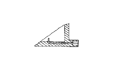
The invention concerns a thermoplastic housing designed to hold electronic
and/or micromechanical components and into which metal conductor tracks pass,
the conductor tracks being injection moulded in one of the housing walls. The
thermoplastic has a flexural strength of at least 200 MPa.


French Abstract

La présente invention concerne un boîtier destiné à recevoir des composants électroniques et/ou micromécaniques. Il est fait d'une matière thermoplastique dans laquelle passent des tracés conducteurs métalliques qui, à cette fin, sont injectés dans une paroi du boîtier. La matière plastique présente une résistance à la flexion d'au moins 200 MPa.

Claims

Note: Claims are shown in the official language in which they were submitted.


- 5 -
Claims:
1. A housing which is made of a thermoplastic synthetic material and designed
to accommodate electronic and/or micromechanical components and into
which lead metallic leads which for this purpose embedded in a wall of the
housing by injection moulding,
characterised in that the thermoplastic synthetic material is selected to have aflexural strength of at least 200 MPa.
2. A housing according to claim 1 in which the synthetic material has a flexural strength of at least 250 MPa.
3. A housing as claimed in claim 1 or 2 in which the synthetic material is a PPS.
4. A housing as claimed in claim 3 in which the synthetic material is a glass fiber
filled PPS.
5. A housing as claimed in claim 3 or 4 in which the PPS-based synthetic material
exhibits a flexural strength of 265 MPa.

- 6 -
6. A housing as claimed in claim 4 in which the distribution of the glass fibers in
the synthetic material is isotropic or does exhibit merely a slight anisotropy.

Description

Note: Descriptions are shown in the official language in which they were submitted.


CA 02206097 1997-05-26
Bc97s041 J~WlBelPCTlEPg5~0~461 7t26.05. 1997
Pl ASnC HOUS~NG DESIGNED ~O J~:COi~,MODATE EL~C'rR~NIC AN~JOR
MlC:ROlJ11~C;H~,Nl~At. I:~OMpoNENT5 ANl~ INTO WHI~I COND~ICl OF~
TRACKS PASS.
5 The invention c~ el ns ~ ousin~ rnade of a U ,~r"~o~ lasti~ synthelic mat~orial d~-
signed to ~,n~nodate ele~roni~ andlor n~'cru~,ec~anic~l oo~ G~ ts and into
which l~ad m~taTlic leads which for this purpose ~re ~n-hecl~ed in a wall of th~h~usin~ by in;ec~ion mouldin~. In certain applications such housin~s ha\~e lo beh~rn~ic ~lly sealed. The l~ ior, where the le3d~ t~ave~se a wall of the h~usin~
1û c~nstlt~e~ a criti~l locali~- For the se~lin~ of the housing. Oflen such leads are
~ormed by punchin~ of metallic strips t~ a latticc whicl~ i8 pos~tion~ in ~n inie~
tion rnold for moul~in~ a p~rt of the housing so that the lattic~ be~".~s partly ~m-
bedded by i,; ~tion nlould;n~. l'h~ m~allic strip may consist o~ copper which is~ oated with alumini~. DifficulUes arise h~m the fact that rnetals and pla~ti~s dif~
15 fer, ~lo~rkably in their coefr;c ant of ~l~ermal exp~nsi~n. ~Ppper ~or ex~rnple h~as a
~en l of U)e""al e,~ ns;on of 17 x 10~1~Kwhereas the""op~d~lic synthetic
rnater~als typi~ally ~a~ ~ a ~o~r;e;en~ of ll l~r",d~ ~x~ansion be~veen 20 x 1 0~1~K
an~ 30 x 1 ~JrK. Under he~t loa~s which may oc~ur not oniy under certain appli-
c~tion conditions P~t already d~Jring the m~n~fa~t~re R~' th~ llousin~, particularly

-
rto ~ v~ al~e ~ MAK~ + AS~ 10
CA 02206097 1997-05-26
wltil~ adh~sives are being cured and whlie ~mpol~nts 3~e ~ n~;t~d by solder-
in~ tQ leads ~rhich a~e en,b~d~cl ~y ini~ction mouldin3""ed~anical stress6s ~r~
~n~.ale~ in the pEastic "~ . Due to the thsrnlal lo~d the p7~tic n,~t~rial will
slip along the nletallic l~ds. Partly this will result in a di~connection of the pla~tic
5 ~T~t~ l frorr th~ n~etel which i~ thc moo~ cec i~ not too b4d cin~ ~ho ~p
~hi~h is ~orn~ed b~ en the meS~llic surf~oe and 1he pla8tic matcrial i5 sul~i-
cientiy nar~ to gua. ~nlee a wffici~nt sealing ~ffeçt. It ~n~y, hov~vor, happe
that in th~ plastic ,nalerial fi~sures are formed ~ h e~ n~ cro~is~ or at riyht
~n~le~ to ~he ~etalli~ lea~s whereby ac~e~s~s to the g~p ~e~00n the lead and
10 ~h~ pl0~ m~l~l ial are form~d so that the housing will no lon~r b~ ti~ht.
It is well knawn in the 8rt to ke~p the differ~nce be~en the Ulerm~l ~xpan~ion
c~o~,-c ~.,. 1~ of met~ls ~nd pl~stic n,~le~ as l~w as pwsib!o by 8ele~tin~ appr~-
priats ~ate~ials and by sh~pin~ the lead~ so as to Ill;.".~li5~3 ~he ~Lf~3~s ~ r3G;~
th~ le~ds snd the s~Jrroundin3 pl2sti¢ fndlerial~ These measures proove, ho~1Evor~
15 rnerely partly ~ $sful; on the one hand the m~terials cannot ~e ~el~ctad ind~~en~ntly ~ince further uiteria h~ve to be met for e~ .,-pl~ wit~ r~ard ta electric
con~uctivity, surf~ nditi.~-" .,~cchan~ and li.~ 1ll8l stability of ~h~pe, resis-
tanOe ~;ns~ selvents, oil and ~resse, ~nd r~sis~ Palinst a3ein~; on the
other hand U161~ iC~ t~ maker;als, Y~hi~h are filled wlth glass ~bers to20 irnprove their m~h~nic~l and U,~r..,al stsbiiity, mostly show~n allis~lu~ y
Ule~ 11181 ~3A~13l ,~ion ooe~lcient ~vhid~ rn3kes it imposs,~la to sdapt their thermal ex-
pansion ~e~ficient ~ ;lly tc that of the lead~.

CA 02206097 1997-05-26
In ~lew of thes~ Facts it is an obje~t of the ~r~R~I~t in~rention to di~close a po~sibil-
ity how to i~ o~ the ti~yl ~ ss of8UCh h~usln~s.
Aco~rdi.)~ to the pres~nt inverttion this ~bje~ i~ acco.nplished by ~ houslng hav-
ing the features included ir ~im 1. ~n such ~ housing, which is n~3de o~ a ~her-
S mopld~tic synthetic ~--dt~rial ~nd d6si~l ~d to acc~m~)~odate ~ tr~l . C an~or
mlcl ur ,e~l ~a~ lpOI l~r ~t~ and into ~hidl l~ad metallic leads which for this
purpos~ sre ~mbed~e~ in a wall ~ the hou~ing b3~ cliot I mou~d~ng, th~ syn-
th~tic .,lat~r i~l is sel~ d tO h a~e a fl~xural ~r~ h of at le~st 2~0 MPa. Pre-
~errecl embodi~nts of th~ inYention ar~ tt~e ~ubjeot Of the ~epen~ent cl~in s.
10 S- ~prisin~ly it has bee~ found that the tel ~d~ to form fissures, which ext~nd
crosswi~ ~o ~he ieads, is ~e~Jc~, if th~ ~hermoplastic synth~tic n~ ri~l, into
which the le~ds are ~ Le~J~J by in,e ~ lion mouldingt is ~GI~_te~ to h~9Y~ a htgh
f~exural ~ n~ "~r~f~r~bly as ttigh a~ possibl~. A~ ty it is ~3ught to select
a ll IGI ",v,vla~l;c Sr~,th~lic ., Idt~l ial havin~ a flexural 3t~ t h of at least 20~ MPa,
~5 p,~.~Lly nlore lhan ~50 MPa. Parffcul3rly h~hiy ~ pffr~t~ro r~si~,rll thern~o-
p~asti~ n~ 15 like PPS exl~ibit ~IJch hi~h flexural stren~tl~s. Thus hard thermo-
pl~sti~ nnateri~ls on the ~asi~ ~f PPS ~re pr~ d. A PPS ~tlled with ~i~ss fibers
has proven particularl~ us~fu~; SU~t (n~t~rial is distribut~d by P~ILLIPS under the
b aJ~ a~ ~YTON R4XT. ~his matafial ~xhibi~ a flexural ~tf6n~ f 265 MP~ as
20 d~ ined accor~ y to ASTM D6~5S9 P~r~ ariy p~r~d ars ~lass fiber

CA 02206097 1997-05-26
d synthe~ic ~,.c,l~r;~'s ,,n whi~h t~ ~ 9s flbers are d~str~buted isotropically o~
ne~rly i~ 'ly ~n or~r to ~void an anisollv,,s~,~l ooe~i;c ~ nt of lll~r.llal ~xpa~
sion and at the ssrne time t~ get a high flex~ral ~tt ~ ,811,.
It i~ an ~dv. rlt~;6 of the invent;on th~t is even unne~sss~ry to a~l3pt the U ,~ ~, r;ll
5 a~pal~slon ~efr~ciE ~t ~f t~ rnlheti~ pl~stic ,~,~5le~ t~ ~hat ~ the met~llic leads
when s~le~ti.l~ a Uh~r,~ ti~ synthetic ~ t~ri~' with hi~h fle~wral st,e~,lyt~l, n~-
erlhe~ss ti~htly en~h~d~d leads are abt~inable.
~h~ enc,ossd single dr~u~ shOW5 ~ s~ti~llalV~eW of a part o~ a w~tl o~ ~ ho~s-
ing made of ~ ri~id pl~stic material in wni~ a lead in en ~e~d&~. The lead i~
p~rtiy covered witl~ a lay~r of S~K~ pla~ic " Iql~rial havin~ a thicknsss of merely
0.4 mm. Wh~n uslng a pla~Uc n~terial havin~ a flex~Jra~ s~r,gU~ of 19~ MPB
mi~o-fissu~0s have been foun~ In the n4 mm tl-i~l< p1astic l~yer a~ al~ro~
and~or "~ ~tldni~ 4n.~er~ents 1 ad been ~n~e~ed tc) th~ le~ds ~ ~lder-
ing and ~Fter th~ housi~ h~d ~eQn sealed, said mic~o~ sures resulting in 3 k:)8s~5 ~f ~ ss. If, 1~; ~1Jol~, a glass fib~r ~l~led PPS pl~stic m~t~r;~l haYir~ 8neXU
~o~ of 265 MPa w~s ~sed ~uch mic~o-fissures cou~d n~ r b~ discov~
er~d l~e tests have be~n carri~d out with h~u5ings hlle~ ~vith an oil and d~
si~ned to ~ ~ceivc a rni~ o~ ani~R~ a~lwltiul 1 senson
Not~: PPS rneans p~ o,~ e s~lphide

Representative Drawing
A single figure which represents the drawing illustrating the invention.
Administrative Status

2024-08-01:As part of the Next Generation Patents (NGP) transition, the Canadian Patents Database (CPD) now contains a more detailed Event History, which replicates the Event Log of our new back-office solution.

Please note that "Inactive:" events refers to events no longer in use in our new back-office solution.

For a clearer understanding of the status of the application/patent presented on this page, the site Disclaimer , as well as the definitions for Patent , Event History , Maintenance Fee  and Payment History  should be consulted.

Event History

Description Date
Inactive: IPC from MCD 2006-03-12
Inactive: Dead - No reply to s.30(2) Rules requisition 2005-04-04
Application Not Reinstated by Deadline 2005-04-04
Deemed Abandoned - Failure to Respond to Maintenance Fee Notice 2004-11-23
Inactive: Abandoned - No reply to s.30(2) Rules requisition 2004-04-02
Inactive: S.30(2) Rules - Examiner requisition 2003-10-02
Inactive: <RFE date> RFE removed 2002-11-27
Inactive: Office letter 2002-11-27
Inactive: <RFE date> RFE removed 2002-11-27
Inactive: <RFE date> RFE removed 2002-11-13
Inactive: Office letter 2002-11-13
Inactive: Adhoc Request Documented 2002-11-13
Letter Sent 2002-11-06
Revocation of Agent Request 2002-10-21
Appointment of Agent Request 2002-10-21
Request for Examination Received 2002-10-21
Inactive: Entity size changed 2002-09-23
Inactive: <RFE date> RFE removed 2002-08-19
Inactive: Office letter 2002-08-19
Revocation of Agent Requirements Determined Compliant 2002-08-19
Appointment of Agent Requirements Determined Compliant 2002-08-19
Request for Examination Received 2002-06-13
Request for Examination Requirements Determined Compliant 2002-06-13
All Requirements for Examination Determined Compliant 2002-06-13
Revocation of Agent Request 2002-06-13
Appointment of Agent Request 2002-06-13
Inactive: Single transfer 1997-11-20
Inactive: First IPC assigned 1997-08-15
Inactive: IPC assigned 1997-08-15
Inactive: Courtesy letter - Evidence 1997-08-12
Inactive: Notice - National entry - No RFE 1997-08-06
Application Received - PCT 1997-07-31
Application Published (Open to Public Inspection) 1996-06-06

Abandonment History

Abandonment Date Reason Reinstatement Date
2004-11-23

Maintenance Fee

The last payment was received on 2003-10-29

Note : If the full payment has not been received on or before the date indicated, a further fee may be required which may be one of the following

  • the reinstatement fee;
  • the late payment fee; or
  • additional fee to reverse deemed expiry.

Patent fees are adjusted on the 1st of January every year. The amounts above are the current amounts if received by December 31 of the current year.
Please refer to the CIPO Patent Fees web page to see all current fee amounts.

Fee History

Fee Type Anniversary Year Due Date Paid Date
Basic national fee - small 1997-05-26
MF (application, 2nd anniv.) - small 02 1997-11-24 1997-10-28
Registration of a document 1997-11-20
MF (application, 3rd anniv.) - small 03 1998-11-23 1998-11-16
MF (application, 4th anniv.) - small 04 1999-11-23 1999-11-16
MF (application, 5th anniv.) - small 05 2000-11-23 2000-11-03
MF (application, 6th anniv.) - small 06 2001-11-23 2001-11-01
Request for examination - standard 2002-06-13
MF (application, 7th anniv.) - standard 07 2002-11-25 2002-09-13
MF (application, 8th anniv.) - standard 08 2003-11-24 2003-10-29
Owners on Record

Note: Records showing the ownership history in alphabetical order.

Current Owners on Record
DODUCO GMBH
Past Owners on Record
ANDREAS KUHNLE
FRANZ KASPAR
Past Owners that do not appear in the "Owners on Record" listing will appear in other documentation within the application.
Documents

To view selected files, please enter reCAPTCHA code :


To view images, click a link in the Document Description column. To download the documents, select one or more checkboxes in the first column and then click the "Download Selected in PDF format (Zip Archive)" or the "Download Selected as Single PDF" button.

List of published and non-published patent-specific documents on the CPD .

If you have any difficulty accessing content, you can call the Client Service Centre at 1-866-997-1936 or send them an e-mail at CIPO Client Service Centre.


Document
Description 
Date
(yyyy-mm-dd) 
Number of pages   Size of Image (KB) 
Representative drawing 1997-09-14 1 3
Description 1997-05-25 4 161
Abstract 1997-05-25 1 9
Claims 1997-05-25 2 28
Drawings 1997-05-25 1 5
Reminder of maintenance fee due 1997-08-02 1 111
Notice of National Entry 1997-08-05 1 193
Courtesy - Certificate of registration (related document(s)) 1998-03-24 1 118
Reminder - Request for Examination 2002-07-23 1 127
Acknowledgement of Request for Examination 2002-11-05 1 177
Courtesy - Abandonment Letter (R30(2)) 2004-06-13 1 167
Courtesy - Abandonment Letter (Maintenance Fee) 2005-01-17 1 175
PCT 1997-05-25 7 239
Correspondence 1997-08-11 1 37
PCT 1997-07-30 8 278
PCT 1997-05-25 22 965
Correspondence 2002-06-12 2 66
Correspondence 2002-08-18 1 17
Correspondence 2002-08-18 1 20
Correspondence 2002-10-20 2 62
Correspondence 2001-01-25 1 19
Fees 2003-10-28 1 41
Fees 1999-11-15 1 38
Fees 2002-09-12 1 42
Fees 1997-10-27 1 44
Fees 1998-11-15 1 42