Note: Descriptions are shown in the official language in which they were submitted.
CA 02206677 2001-04-04
70128-329
BURST-ERROR RESISTANT ATM MICROWAVE
LINK AND NETWORK
Field of the Invention
This invention relates to the field of
telecommunication networks and packet switching and in
particular to providing reliable radio-based links for cell and
frame-switched networks.
Cell-based packet switching networks are becoming
widely available. The use of small (i.e. "short") packets of
information is preferred in modern digital networks because it
enables the efficient mixing of synchronous and asynchronous
information, thus providing cost-effective transport of digital
voice, LAN data and video. Furthermore, short packets, also
known as "cells", can be switched by integrated circuits,
allowing quick and economical switching of data in broadband
fiber optics networks. This concept is known in the telecom
industry as "Asynchronous Transfer Mode" (ATM). ATM networks
are commercially available. ATM protocols have been formalized
by various international organizations, including the ITU and
the ATM Forum. ATM networks were specified assuming the use of
fiber optics links for transmission. Due to the very low bit
error rate of fiber optic links, ATM networks do not provide
extra overhead services to guarantee end-to-end delivery of
cells. Cells are routed through the network, but if an error
occurs (or a buffer overflows), cells may be discarded. The
simplicity of "best effort" cell delivery results in a fast and
cost effective network.
1
CA 02206677 1997-06-02
WO 97/13292 PCT/US96/15418
Typical fiber networks consist of long-haul fiber
links interconnecting ATM switches. These switches may
be connected by fiber optics links to customer sites,
such as office buildings and homes. In the customers'
buildings there are network access nodes that combine
and convert a user's information to ATM cells for
transmission over the network.
Although fiber optics links are becoming the
preferred medium for terrestrial links, they are not
always available. City regulation, installation costs,
long installation time and legal right-of way issues
prewer~t some regions from irstqlling fiber optics
links. Some cities may have fiber optics links
installed, but owned by a monopoly which a service
provider may wish to bypass.
Digital microwave radio links can provide an
alternative to fiber optics links between network
access nodes and ATM switches. Frequency bands within
the range of about 300 MHz to 60 GHz have been
allocated for commercial communications. Some
microwave links in the millimeter wave region are
unlicensed or licensed for low usage fees by the local
authorities. Microwave radio links then become a cost-
effective and a timely solution to the deployment of
telecommunication links. There is a drawback, however,
to these microwave radio links. Digital microwave
radio communication is prone to bit errors, especially
under weather-induced fading conditions, such as rain.
Some forward error correction, redundancy and
retransmission protocol schemes have been devised to
improve the performance of microwave links. The
problem with these approaches is that they are not
directly applicable for ATM, Frame Relay and similar
types of packet switched traffic. Retransmission is
unacceptable because of the delay it introduces.
Forward error correction alone does not protect from
-2-
CA 02206677 1997-06-02
WO 97/13292 PCT/US96/15418
antenna obstruction or antenna failure. Redundancy by
parallel links is too costly and still prone to common
link obstructions such as weather-induced signal
' degradation. These problems have been addressed by our
above-mentioned application. However there are other
problems that the previous application does not
address. The actual migration to ATM-based networks is
a gradual process in which non-ATM traffic may co-exist
with ATM traffic. For example, a customer premises
site may desire to connect four E1 lines to the point
of presence, wherein one E1 carries digital voice
(Poise code t~iodulation - PCM) from a switch (Private
Branch Exchange - PBX) using non-ATM primary rate ISDN
format. Another E1 may carry data from a router or a
concentrator, following frame relay format. Yet
another E1 may include ATM-like protocols that do not
conform with a standard ATM format, intended for trunk
connection between similar switches, and finally the
fourth E1 may be standard ATM, complying with the ATM
forum. These lines need to be combined on a single
radio link, each receiving the quality of service
appropriate to the type of information it carries.
Frame-relay and ATM-like protocols are all based on
transmission of packets of variable or fixed size,
commonly referred to below as "frames". These frames
may have error check words to allow the receiving
system to reject frames containing errors. However,
there is a small probability that a frame will contain
errors, yet the checksum will be valid. Whenever a
burst error occurs that a forward error correction
system cannot correct, the frame is delivered with the
error. If the checksum appears valid, the frame may be
delivered to the wrong address, a process called
"misinsertion". Another problem with current
approaches is the lack of standard methodology for
forward error correction (FEC). FEC requires expensive
-3-
CA 02206677 1997-06-02
WO 97/13292 PCT/US96/15418 -
digital circuitry. Cost could be reduced if the
transmitted information format could rely on FEC
technologies available for mass markets.
Yet another problem is the reusability of a radio
system for changing needs. Installing a radio system on
a roof of a building is expensive. When user
requirements are changing, for example a higher data
rate is desired, a new outdoor radio unit needs to be
installed. This also is forcing the network integrator
to store many varieties of radio units, differing in
frequency channel, data rate and modulation scheme.
Summary of the Invention
This invention provides burst-error resistant
microwave radio-based communication links for ATM and
non-ATM transmission.
In accordance with this invention, a cell-based
access network is formed to connect multiple customer
sites to a switching center. The network as a whole,
and each link in this network, are especially designed
to provide reliable service under bit-error conditions.
In accordance with one embodiment of this
invention, at the link level, reliable service is
provided by subsystems called "Trunk Units" (TU) which
process information before and after transit through
the error-prone radio link. At the transmit side, the
TU first multiplexes bit streams from multiple inputs
into a combined bit stream using time division
multiplexing. Then the TU splits the information to be
transmitted into blocks of a fixed size. These blocks
are encoded for forward error correction (FEC). If bit
errors occur in a block, the FEC decoder circuit
normally corrects them. If the errors cannot be
corrected by the FEC circuit, an indication is passed
to a Payload Processing Module (PPM) circuit that can
be customized to be compatible with the switch
-4-
CA 02206677 1997-06-02
WO 97/13292 PCT/US96/15418 -
manufacturer, which depending on the type of connection
in each line either:
- passes the error-containing information unchanged or:
- modifies the information content to ensure that it
will not be misinserted.
' The misinsertion protection is provided to streams
containing ATM, frame relay or similar frame-based
protocols. Misinsertion protection is provided by
modifying the data with abort sequences (for High-Level
Data Link Control (HDLG)-like protocols), or by
deliberately corrupting the error checksum of either
tha ATM header or High-lwel Data Link Control (HDLG)
frame, as appropriate. The networking equipment will
automatically reject such corrupted frames.
To come up with a cost effective FEC circuit, this
invention uses the FEC block format that conforms with
standards used for Digital Video Broadcasting (DVB).
DVB circuits use Reed Solomon (RS) code with
interleaving and in combination with Viterbi
convolutional decoder. The combined Viterbi-RS code is
known as a concatenated code. The Viterbi
convolutional code and the interleaving functions are
not desired for wireless ATM and telephony applications
because they use extra bandwidth and delay,
respectively. Therefore these functions are normally
bypassed, but are optionally included if further error
correction performance is desired at the expense of
bandwidth (Viterbi) and delay (interleaving).
The generality of the Radio Unit in accordance
with this invention is provided by the use of a linear
transmission scheme on the outdoor part. The Radio
Unit is performing translation and amplification with
linear wideband amplifiers of the signal sent from the
indoor Trunk Unit. Therefore various modulation
schemes can be used, such as QPSK, FSK, QAM, MSK or any
other band-limited scheme. The change of modulation
-5-
70128-329
CA 02206677 2001-04-04
scheme requires only a change of an indoor modem.
The radio link as described above can be combined
with other network access systems or alternate links (microwave
relay radios or fiber optics links) from a network. The
network, in one embodiment, has a mesh topology, but not
necessarily a full mesh. In other embodiments, single or
multiple rings are also acceptable topologies. The network
links bit rate is higher than the total bit rate of the user
information transmitted via these links. The extra bandwidth
of the network links allows protection bits to be carried that
add protection to the information being transported via the
microwave network.
The invention may be summarized as a digital radio
link including: an access unit for transferring data packets of
variable or fixed size to and from a plurality of line
interfaces; a transfer circuit for receiving data from the
access unit including a forward error correction encoder
circuit for forward error correction encoding; a reception
circuit for receiving data packets from the transmission
circuit, said reception circuit including a forward error
correction decoder for indication of an uncorrectable block;
and a payload processing module for receiving bits from said
forward error correction decoder and modifying some of said
bits to reduce the chance of data packet misinsertion.
This invention will be more fully understood in
conjunction with the following detailed description taken
together with the drawings.
Drawings
Figure 1 shows a wireless network of a type suitable
for use in a city.
6
70128-329
CA 02206677 2001-04-04
Figure 2 shows the basic building blocks of a point-
to-point access node of this invention.
node.
Figure 3 shows a physical implementation of an access
Figure 4 illustrates a product family based on the
protected link of this invention.
Figure 5 illustrates attachment of an access node of
this invention to different networking systems.
Figure 6 illustrates a block diagram of an access
node's Network Access System of this invention.
Figure 7 illustrates processing of Frame Relay or
similar frame-based data in this invention.
invention.
Figure 8 illustrates Processing of ATM cells in this
Figure 9 illustrates a block diagram of the transmit
side of the Payload Processing Module.
6a
CA 02206677 1997-06-02
WO 97/13292 PCT/US96/15418
Figure 10 illustrates a block diagram of the
receive side of the Payload Processing Module.
Figure 11 is a block diagram of a linear radio
unit suitable for use with this invention.
Detailed Description
Certain abbreviations used in this application
are
defined below.
AN Access Node
ARQ Automatic Retransmit Request
ATM Asynchronous Transfer Mode
AU liccess Unit
CU Control Unit
CRC Cyclic redundancy code
DC direct current
DVB Digital Video Broadcast
E1 European digital line interface at
2.048 Mbps.
E2 European digital line interface at
8.448 Mbps.
E3 European digital line interface at
34.0368 Mbps.
EPROM Erasable Programmable Read-Only Memory
EEPROM Electrically-Erasable Programmable
Read-Only Memory
FEC Forward Error Correction
FPGA Field programmable gate array
FSK Frequency shift keying
HDLC High Level Data Link Protocol-a
bit-oriented synchronous link layer
protocol
HEC Header error control
IP Internet Protocol
LAN Local Area Network
LED Light Emitting Diode
LNA Low Noise Amplifier
CA 02206677 1997-06-02
WO 97/13292 PCT/LJS96/15418
Mbps Mega bits per second
MHZ Mega Hertz
MIB Management information base
MMIC Monolithic Microwave Integrated Circuit
MSK Minimum shift keying
NAS Network Access System
NMS Network Management System
PBX Private Branch Exchange, a generic term
for a voice switch
PCM Pulse Code Modulation
POP Point of presence
FPM Payload Processing module
PROM Programmable Read-Only Memory
PTT Post Telephone and Telegraph, a common
name for government service providers
QPSK Quadrature phase shift keying
QAM Quadrature amplitude modulation
RU Radio Unit
RS Reed Solomon
SNMP Simple Network Management Protocol
STM Synchronous Transfer Mode
Terminal A system consisting of NAS,RU and the
interconnections
TMN Telecommunications Management Networks
TU Trunk Unit
VCI Virtual channel identifier
VPI Virtual path identifier
X.25 An international user-network data
communication interface standard
A metropolitan
area network
in accordance
with
this invention
is shown in
Figure 1. The
dark arrows
l0a through
lOh represent
wireless links
with radio
transceivers (not shown) at each end. These wireless
links connect buildings shown as lla through lij in
a
city to a central
office 14 also
called a "point
of
presence". The
point of presence
14 ("POP")
includes
_g_
CA 02206677 1997-06-02
WO 97/13292 PCT/US96/15418
ATM switches, frame relay datacom (X.25) switches and
voice switches. This invention allows exchange of
digital voice and data between these switches and makes
available ATM developed for fiber optics for
transmission by digital radio. A network allows the
extra benefits of relaying information from remote
stations such as at location 15, even if the remote
stations have no direct line of sight to the point of
presence 14, as well as providing redundant links, and
the ability to concentrate information from multiple
nodes.
The minimum access node far a pci:~t-to-point link
of this invention is depicted in Figure 2. This
minimum system is sufficient if the advantages of a
full network are not required or if networking
equipment is already available and wireless link
extension of this networking equipment is desirable.
An access unit (AU) is capable of interfacing with a
variety of local interfaces. In the AU, the signals
from these interfaces are either converted to ATM
cells, which are delivered to a trunk unit (TU) or are
kept in the original format for time division
multiplexing at the TU. A suitable AU can be purchased
today from a large number of vendors, for example ADC-
Kentrox of Portland, Oregon. In the preferred
embodiment, an Access Unit comprised of four E1
interfaces is used. An appropriate AU can be designed
as a set of electronic cards and software, as described
below. A non-ATM AU may consist of an interface IC
for, say, E1 line, providing data and clock lines to
the Trunk Unit. A non-ATM AU can still carry ATM
traffic originating in external ATM equipment that maps
ATM cells onto E1 physical layer interfaces. The TU
includes the Payload processing Module (PPM) that can
identify cell or frame boundaries, encapsulate the
cells if so desired and deliver them to a multiplexer.
_g_
CA 02206677 1997-06-02
WO 97/13292 PCT/US96/15418 -
A TDM multiplexer in the TU combines the user bit
streams, adds FEC and other overhead and modulates the
aggregate bit stream for transmission. The TU and PPM
are key elements of this invention. The TU outputs a
modulated serial bit stream to the radio unit (RU)
which is placed on the outside wall or roof of a
building, attached to a dish antenna. A twisted pair
cable, coax or fiber optics link connects the RU to the
TU. The RU up-converts the modulated bit stream and
transmits it at the desired microwave frequency. This
system operates normally in a full-duplex mode; thus
the RU also receives a bit stream from an opposite
access node and delivers this bit stream to the TU.
The TU processes this received bit stream, including
error correction and using the PPM to mark the dropping
of cells or frames that are included in non recoverable
FEC blocks. The TU delivers good cells to the AU and
logs or reports cell loss to a Control Unit (CU) - a
microprocessor circuit.
A physical implementation of this system is shown
in Figure 3. A Network Access System 30 ("NAS") is
built into a metal enclosure. The E1 interfaces are
provided by connectors, such as BNC 31. Other
connectors 32 allow NMS and user access. An On-off
switch 33 controls power and an LED 34 displays power
state. Other displays 35, 36 allow monitoring of link
condition, the transmitted frequency or any other
desirable condition. A coax cable 37 connects the NAS
with the RU 38. A dish antenna 39 attached to the
30 RU provides transmission to and from the remote side of
the link. This system, combining NAS 30 and RU 38 is
also shown in Figure 4.
Other products can also be built on the principles
of this invention. When access functions are desired,
converting non-ATM traffic to ATM and multiplexing it
with other ATM traffic, an integrated access node 41
-10-
CA 02206677 1997-06-02
WO 97/13292 PCT/US96/15418 -
can be provided. This access node 41 includes ATM
access technology which is available from other sources
(as mentioned above), and the TU, CU and RU 32 of this
invention. The TU can be implemented as a plug-in unit
44 into the backplane of such access node 41. If ATM
switching is desired, multiple such RUs 28 can plug to
multiple TUs 45a, 45b in a switching system 46. A
network management system workstation 47 controls and
configures the above systems. A communication protocol
is established between each unit 30,41,46 and the
workstation 47. SNMP protocol and a management
information base (MIE) are a common v~ay of managing
such a network. It should be clear that a network may
consist of a plurality of either one or more types of
systems 30, 41 or 46.
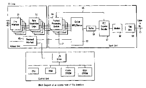
Figure 5 depicts a four-E1 access node connected
to different sources of information. This
configuration is arbitrary; the NAS 50 can handle any
combination of traffic types or equipment types. The
NAS 50 is connected to a PBX 51 that provides PCM voice
over the E1 interface. This voice is transmitted
transparently via the NAS without extra protection.
The FEC of the NAS normally provides error-free
operation. If occasional burst errors occur which the
FEC cannot correct, the user may hear some noise, which
has little effect on the overall link quality. Another
E1 port may be connected to an ATM switch 52 with
proprietary ATM traffic. A proprietary ATM link does
not adhere to an industry standard, however if the
switch vendor agrees to specify the cell or frame
format, the link can be given special treatment by the
NAS. Since proprietary ATM links are similar to either
standard ATM or to frame relay, the treatment of these
links is a straight-forward generalization of the frame
relay and ATM interfaces to be discussed below. The
third interface is connected to a frame relay router
-11-
CA 02206677 1997-06-02
WO 97/13292 PCT/US96/15418
53. Frame relay 53 is based on HDLC frames embedded in
an E1 interface. When a frame relay frame is subject
to a burst error in the radio link which FEC cannot
correct, a misinsertion may take place. Misinsertion
means that the frame may arrive at a different address,
perhaps the address of a competitor of the original
user. This event should be quite rare, because most
frames containing errors will be rejected by the frame
relay network equipment, because a frame containing
errors will have a non valid CRC checksum. However a
16-bit CRC under burst error has a probability of about
one in 65,000 to check valid despite the error. A
network with a total throughput of billions of frames
per day may have enough burst errors that some frames
will be misinserted. Similarly, an ATM source 54 may
have its ATM cells subject to uncorrectable burst
errors and misinsertion. The NAS structure to handle
such a mix of traffic is shown in Figure 6. An access
unit includes a plurality of line interfaces 61 (four
in this example). Each line interface 61 converts one
full-duplex E1 to NRZ clock and data signals. Such
devices are available from many vendors, including
Crystal Semiconductor Corp. of Austin, TX. These bit
streams will be time division multiplexed by a digital
multiplexes 62 but since each E1 differs slightly in
its clock rate, the E1 rate is adapted to the
multiplexing rate by rate adaptation logic 63. This
logic is similar to the functions done by T1 to T3
multiplexers which are well known. The multiplexing
clock rate is nominally higher than the E1 clock by a
few percent. Bit stuffing, stuff indication and
framing are included in the multiplexing scheme, as is
customary with such multiplexers. A payload processing
module ("PPM") 64 performs the burst error protection
processing, as discussed below. The interconnect lines
in Figure 6 represent bi-directional connections; thus
-12-
CA 02206677 1997-06-02
WO 97/13292 PCT/US96/15418
the PPM 64 performs both the transmit and receive
functions, as discussed below. The multiplexer 62
combines all of the PPM outputs and overhead bits (for
NMS or similar functions gathered by an overhead
interface 65) to a buffer 66. The buffer 66 is
- required because the next stage, FEC 67, must delay the
inputting of data for transmission of an error
correction checksum. FEC encoders and decoders are
available in many forms; however the preferred
embodiment uses a Reed Solomon (RS) code with block
size 204 bytes and data size of 188 bytes. The
overhead is thus 16-bytes, which allows correction of
up to eight bytes containing errors. If more than
eight bytes contain errors, the decoder cannot correct
the error. The decoder can indicate that an
uncorrectable error has occurred. Due to the internal
delaying of data for error correction purposes, the
decoder can indicate the error at the same time that it
outputs the data at its port. This indication is
connected by conductor 68 to the PPM. An RS decoder
may occasionally misinterpret a block containing large
errors as a correctable one, but this event has a low
probability. With the (204,188) block size, the
incorrect decoding probability is estimated as
approximately one in 300,000, which is the ratio of
valid or correctable blocks to the total number of
possible blocks. This is the net gain in burst error
protection, i.e. an FEC-protected link with a PPM of
this invention is roughly 300,000 times less likely to
cause misinsertion as the same link without a PPM. The
RS (204,188) code was standardized by the European
Broadcasting Union specification DT/8622/DVB which is
related to direct satellite video broadcast. The
advantage of such an approach is the availability of
integrated circuits for this function at high-volume
and low cost by multiple vendors, including AHA of
-13-
CA 02206677 1997-06-02
WO 97/13292 PCT/US96/15418 -
Pullman, WA, LSI Logic of Milpitas, CA and VLSI
Technology of San Jose, CA. Most vendors provide a
decoder only because it is also the mass market part in
broadcasting. Fortunately, this is also the more
complex part. Some vendors, including LSI, also have
an encoder. Furthermore, the ICs include descrambling
and framing of the FEC frame, further simplifying the
implementation of a link. An example of a decoder chip
is AHA4210. The frame generation and scrambling can be
implemented by feedback shift-register techniques which
are well known in the art of digital design. Since
encoder designs exist, some of the above vendors
provide such designs for custom logic of field
programmable gate array implementation. Some FEC
decoders do not allow bypassing the Viterbi decoder.
It would be a simple technical task to request these
vendors to modify the design to exclude the Viterbi
Decoder, but it could be costly. Therefore, if the
Viterbi decoder cannot be bypassed, a dummy Viterbi
code can be emulated to gain access to the RS decoder.
This is done as follows. The received digital
information from the modem is byte-synchronized using
the dedicated synchronization byte in the FEC block, or
by phase-shifting a bit clock divided by eight until
the RS decoder will lock. Once byte synchronization is
accomplished, the bit stream is Viterbi encoded. A 2:1
encoding requires doubling of the bit clock; this can
be done by a frequency doubler. Another code gain,
such as 7:8 can be used, but is slightly more difficult
to implement. The Viterbi encoder is made of eight D-
flip flops and feedback logic, as described in error
correction literature. The encoded bit stream enters
the FEC decoder which "decodes" the Viterbi code
without errors (the local digital connection from the
Viterbi encoder to the FEC decoder is practically
error-free). The rest of the decoding continues
-14-
CA 02206677 1997-06-02
WO 97/13292 PCT/US96/15418
normally.
The FEC-encoded bit stream is driving a modem 68.
This is a carrier-based QPSK modem. QPSK modem ICs are
available off the shelf from LSI Logic, Plessey and
Maxim. The modem transmit carrier is about 200 MHz and
the receive frequency is 70 MHz. These frequencies are
only examples, and their exact value may be adjusted to
obtain a combination with minimum harmonic
interference. Other modem types are possible. When
bandwidth is critical, a QAM modulation may be chosen.
The modem output is connected to a frequency division
multiplexer ~64, which consists of bandpass filters; one
for each frequency involved. In addition to the 70 and
200 MHz mentioned above, a low frequency (say, 10.7
MHz) may be used for a data link with the RU
microprocessor, via a small modem not shown in
Figure 6. DC power may be sent to the RU via the cable
70 and a low-pass filter.
The receive side is similar in construction. The
data received by the modem 68 is connected to the FEC
decoder 67. The data flows towards the E1 interfaces
via the other processing blocks as shown. The control
unit is a microprocessor board with software embedded
in a boot EPROM, flash EPROM and RAM. The flash EPROM
allows remote software upgrade via the NMS. The CPU
board communicates with the system via I/O drivers.
Only one I/O line 71 is shown, but almost every complex
device is connected to the CU for configuration and
alarm monitoring purpose.
The processing steps of frame relay or similar
type of frames are shown in Figure 7. HDLC frames 72
are generated in outer equipment for transmission. The
frames are separated by at least one flag (01111110
symbol) according to the HDLG protocol. Thus a
following frame 73 could originate from another user.
The network can route frames to their destination based
-15-
CA 02206677 1997-06-02
WO 97/13292 PCT/US96/15418
on address bits included in the frames. These bits
usually indicate a virtual link number which is used by
routing tables in the Frame Relay Network to route each
frame to the next network node until it reaches its
destination. This process takes place in routers or
frame relay switches and is normally done outside the
equipment of this invention. The frames are usually
embedded into an E1 frame so that they can be sent over
E1 transmission facilities. The frame 72 could be
mapped onto an E1 frame, occupying the gray area 74 in
the E1 frame. The HDLC frame 74 is interrupted
periodically by E1 framing byte 75. This E1 interface,
including its frame relay payload, is input to the NAS
of this invention. For frame relay payload, the PPM
transmit side in a preferred embodiment is transparent.
The entire E1 bit stream, including E1 framing, is
multiplexed with other PPM outputs, as was shown in
Figure 6. The multiplexer output is then buffered and
FEC check word (16 bytes)76 is appended. The combined
transmission is called an "FEC block". It includes
synchronization bits 77 that indicate block
starting/ending and bit stuffing for the rate
adaptation of each E1 line or other multiplexed
tributary. These FEC blocks are usually received at
the remote side of the link without errors. If a few
errors occur, the FEC decoder corrects them. If more
than 8 bytes contain errors in an FEC block, the FEC
decoder is unable to correct the data. It can only
indicate by a signal 78 that starts at the beginning of
the block that the following block contains
unrecoverable errors. A typical digital radio not of
this invention usually delivers the block with the
errors to the output. However if a burst error
corrupts parts of a frame 79, the flag 700 separating
frames 72 and 73 may be eliminated by the error 79;
thus the two frames may appear fused together as an
-16-
CA 02206677 1997-06-02
WO 97/13292 PCT/US96/15418 -
enlarged frame 701. This combined frame appears to the
network as a valid frame having the address of the
first frame 72 and the CRC of the other frame 73 (HDLC
frames have the address at the beginning of the frame
and CRC at the end). Thus, if the CRC happens to check
valid, the combined frame will be routed to the
destination of customer A, but customer A will also
receive an attached frame 73 of an unrelated user. If
this frame contains ASCII text of a competitor, heavy
business damage could result. This invention ensures
that these frames will all be rejected by the Frame
Relay network. Tris is accomplished at the receive-
side PPM by writing a abort sequence 702 consisting of
seven or more "ones". These aborts are injected after
every flag whose following frame overlaps an FEC block
containing errors 78. If the outside equipment does
not tolerate the abort sequence (it may be designed to
go out of service for a period of time) then an
alternative abort method of the PPM of this invention
is to buffer the bit stream for the depth of the CRC
word size (16-bits), to deliver each frame with the
errors, but to invert the last bit of the CRC code
anytime it checks "valid" without this invention. The
process just described is done on each tributary
containing frame relay or similar HDLC-based
information. A similar process takes place for ATM
traffic.
As shown in Figure 8, the ATM cells 80 and 81 are
of a fixed size (53 bytes) including a 5-byte header
with a virtual path virtual circuit field (VPI/VCI)
that is shown here as an address field 82. An eight-
bit header error control code 83 (HEC) is also present.
The ATM cells are mapped onto an E1 bit stream 84
according to ATM standards. This is the way the ATM
cells enter the NAS of this invention in the preferred
embodiment. Inside the NAS, the bit stream 84 is
-17-
CA 02206677 1997-06-02
WO 97/13292 PCT/US96/15418
delivered to the PPM transmit side, which may append an
extra CRC code. This code adds about 1.8% of bandwidth
per each extra CRC byte, which increases slightly the
radio link bandwidth, but may be acceptable in many
applications. This CRC is only an option. The
multiplexing to an FEC block is similar to the frame
relay application and both may co-exist in separate
tributaries. If an ATM cell is received with an error
86 that might have damaged the address 82, then this
cell will normally contain a non-valid HEC byte 83.
However, one of 256 such cells could be check valid
despite an error. There is no risk of fusing two cells
like the frame relay case, but a cell can be
misinserted and delivered to another service not
related to the original destination. If the other
service is error sensitive, such as compressed video or
constant bit rate service, the insertion of a cell not
related to that service will cause interruption of that
service. A misinserted cell can travel in the network
and cause an interruption of service in areas not
expecting such events. Given the large number of cells
traversing an ATM network, this phenomenon is quite
likely. Misinsertion can affect the quality of service
for the entire ATM network, not just for the link
containing errors. Once an uncorrectable error has
been detected by the FEC decoder, all cells included in
this block are marked to be rejected. The marking
involves the inversion of the last HEC bit in the event
that if and only if this HEC would check "valid"
without the inversion and this cell is desired to be
rejected. The optional extra CRC 85 and 88, can
further improve performance. As mentioned above, the
FEC decoder can occasionally incorrectly decode an
error. The CRC may still indicate that the last cell
contains error; thus it may further reduce the chance
of misinsertion. Using this CRC option, a cell is
-18-
CA 02206677 1997-06-02
WO 97/13292 PCT/US96/15418 -
marked for rejection if either an FEC block indicates
uncorrectable error or a CRC error has been detected.
Alternatively, one may use the CRC to reduce the
number of lost cells. In this alternative, a cell is
marked to be dropped if both the CRC and the FEC blocks
indicate an error. Since the CRC is appended to a
single cell, only this cell will be dropped; thus a
burst error affecting one cell does not cause the loss
of other cells of the same FEC block. The PPM of the
preferred embodiment can perform both options. The
choice is done by software configuration. The trade-
aff between extra cell loss and reduction of
misinsertion probability is left to the system
operators.
A third option is not to include the extra CRC.
The need to check the CRC causes extra delay of about
one cell which may be considered a poor trade off.
After describing the process of protecting frame
relay and ATM cells, the PPM implementation is straight
forward. A transmit side PPM is shown in Figure 9.
The transmit side appends the CRC to ATM cells and not
to frame relay frames. An E1 frame monitor detects the
framing byte of the E1, allowing separation of the
payload frames/cells from the E1 bit stream. An off
the shelf E1 framer can be used, such as Dallas
Semiconductor of Dallas, TX DS2153Q. In a preferred
embodiment, this function is performed by a field
programmable gate array (FPGA). The next step is a
cell/frame delineator. For frame relay, this system
detects flag symbols according to the HDLC protocol.
The contiguous non-flag bits between two flags are
considered "frames" and can be appended with an extra
CRC. For ATM, cell delineation is done by searching
for a byte position that results in valid HEC code for
several consecutive 53-byte cells. This process is
well documented in ATM standards. The delineated cells
-19-
CA 02206677 1997-06-02
WO 97/13292 PCT/US96/15418 -
are then appended by a checksum calculator, preferably
a CRC 8-bit code. A buffer holds the data while the
CRC is being transmitted. A multiplexer selects
between the data and the CRC. Obviously, the
multiplexer's bit rate is increased by the added CRC
overhead. The entire PPM section of Figure 9 can be
implemented by a field programmable gate array, such as
EPF8820A made by Altera of San Jose, CA. In fact, this
circuit should occupy a small fraction of such an FPGA,
allowing integration with the digital functions of the
NAS.
As mentioned earlier, the PPS transmit side is
optional. The receive side performs the main
misinsertion protection process. The receive PPM is
shown in Figure 10. Similarly to the transmit side, it
includes an E1 frame monitor and a cell (ATM) or frame
(frame relay) delineator and a checksum calculator for
the extra CRC in the ATM CRC option. This block may
also calculate the HEC for ATM cells or the CRC of HDLC
frames. The error message 78 from the FEC block is
delayed by a delay equalizer (a shift register) to
equalize the error indication arrival time with the
processing delay of the PPM. A frame rejection marker
controls the marking of a frame or cell. For ATM cells
this marker identifies the location of the last bit of
the HEC, and it enables inversion of that bit if and
only if this cell came from an error-containing block
and the HEC checksum is valid. Alternatively, this
block can be implemented to reject a cell only if the
extra CRC is non-valid. In the case of frame relay,
the frame rejection marker specifies the time at which
an abort sequence of multiple ones will be issued. As
mentioned, this will happen during all frames detected
while an FEC error block indication 78 is received. A
buffer allows for the omission of extra CRC bits if
that option is implemented. A gate performs the actual
-20-
CA 02206677 1997-06-02
WO 97/13292 PCT/US96/15418
marking. For bit inversion in ATM this is simply an
exclusive OR gate. For HDLG abort it is an OR gate.
Finally, a demultiplexer actually removes the optional
CRC (if included) from the ATM cells.
Although not shown in the figures, it is customary
with good engineering practice to store exceptional
events such as uncorrectable error or the marking of an
ATM cell for rejection in a register that can be
addressed, read and cleared by the CU for reporting to
the NMS. Also not shown but implemented are interface
means to the CU by which the system is configured to
operate in ona protocol mode or another. These
indications are usually done via configuration
registers. An advantage of this invention is its
transparency to the user's bit stream. All of the
above processing does not alter the order or content of
bits received at the NAS input to that delivered at the
remote NAS output. The only intervention with the user
stream is the occasional insertion of abort or bit
inversions. This allows the system to operate in an
automatic mode. As a new E1 port is activated, its bit
stream is transmitted to the other side of the radio
link. Once the PPM circuitry gains E1 frame
synchronization and cell/frame delineation, it may
start performing the misinsertion protection functions.
If a PPM circuit fails to synchronize, the protection
function is lost, but there is no interference with a
user's traffic. Furthermore, this invention allows
automatic detection of the protocol, assuming that the
input protocol is one of a known set of distinct
protocols. For example, supposing that the protocol
can be either ATM, Frame Relay or PCM voice. The CU
can start a protocol search by instructing the PPM
receive side to look for ATM delineation. In
successful, ATM is presumed and the process stops. If
ATM delineation is not detected, the PPM is instructed
-21-
CA 02206677 1997-06-02
WO 97/13292 PCT/US96/15418
to search for Frame Relay flags. This process is more
elaborate because random data may also contain "flags".
However a frame relay bit stream will contain
occasionally many flags in sequence, signifying an idle
period. In fact, a queuing system before an HDLC
transmitter does not normally exceed 90% utilization;
thus the flags must be more likely than random data.
Once flags density rule is used to detect this
protocol, abort correction may take place. If none of
the above is present, the link is presumed to be non-
protocol conforming and burst protection is not
provided. The FFri may keep alternating between ATM and
frame relay search modes until a protocol is
discovered. The CU can also be programmed to operate
in a non-automatic mode, in which only one protocol is
chosen for a given interface. The multiprotocol
capability can be implemented in several ways. One
simple way is to duplicate the PPM circuit for each
distinct protocol and enable only the output of a
selected one. In the above example, it is more cost-
effective to implement one generalized PPM with
protocol variations embedded with each PPM block.
A radio unit is shown in Figure 11. A coax cable
from the NAS Trunk Unit carries all the information and
DC power to the RU and the received signals from the
RU. A cable multiplexer 110, identical to the NAS
multiplexer 69 in Figure 6, combines all of the
involved signals (DC power is not shown). The
transmitted signal may be at a frequency of 200 MHz.
It is up-converted by a mixer ill to 2.6 GHz. The
mixer is driven by a synthesizer 113 of 2.4 GHz. Such
synthesizers are commercially available from many
sources, including Communications Techniques Inc. of
Whippany, NJ. The mixed signal is amplified by a
software controlled amplifier to allow power adjustment
depending on the link range. Further conversion steps
-22-
CA 02206677 1997-06-02
WO 97/13292 PCT/US96/15418
are possible until a desired frequency is reached. In
the preferred embodiment one extra conversion takes
place at 36 GHz taken from the 15th harmonic of the
synthesizer 112 by a frequency multiplier 114. A mixer
115 converts the signal to 38.6 GHz, which may be the
desired millimeter wave frequency. A diplexer 116
drives the dish antenna and receives a signal from the
antenna at a different frequency, say 37.4 GHz. The
received signal is amplified by an optional low noise
amplifier 117 to minimize the system's noise figure.
The signal is then down converted to a lower frequency
(in vhis example to 1.4 GHz), filtered in band pass
filter 118 and down converted again to 70 MHz by a 2.1
GHz synthesizer 119. The transmit amplifiers are kept
at a linear mode of operation, allowing the variety of
modulation schemes discussed above. Figure 11 shows
only few of the filters included. It is customary to
use image rejection filters after any frequency
conversion step, as is well known to radio engineers,
but not always shown in Figure 11. Also not shown are
DC power distribution lines and AGC amplifiers that are
typically used in such circuits. All of these features
are well known to radio engineers. A microprocessor
120 controls the synthesizers and checks the integrity
of the RU by measuring voltages in different test
points in the RU. The microprocessor maintains a low
bit rate link with the NAS Control Unit; thus the
frequency and power settings of the RU are controlled
directly by the CU and indirectly by the NMS. Of
particular interest is a tilt switch 121 mounted on the
radio unit. The RU can be mounted vertically or
horizontally, allowing transmission/reception of either
vertical or horizontal radio wave polarization. When
the RU is placed vertically, the tilt switch is off.
When placed horizontally it is on. The RU mounting
hardware (not shown) is designed so that there are only
-23-
CA 02206677 1997-06-02
WO 97/13292 PCT/US96/15418
two possible mounting positions; thus the switch status
is an indication of the polarization. This allows the
microprocessor 120 to read the switch position 121 and
report the polarization to the CU and then to the NMS.
Occasional mounting errors can thus be detected
remotely at a low cost.
Other embodiments of this invention will be
obvious to those skilled in the art in view of this
disclosure.
-24-