Note: Descriptions are shown in the official language in which they were submitted.
CA 02207175 1997-06-OS
WO 96/18131 PCT/CA95/00665
1
OPTICAL WAVEGUIDE CROSS-POINT SWITCH
Field of Invention
This invention relates to cross-point switches and
more particularly to full-broadcast, strictly non-blocking,
h
optical waveguide, cross-point switches, which are compact
and capable of high speed operation.
Background
The telecommunications industry is rapidly
adopting optical transmission networks in order to achieve
the bandwidth necessary to provide video and high speed data
services. It is known that single mode optical fibers have
the potential to propagate data having a bandwidth in the
terabit range. Elements of the network which rely on
electrical input such as switching, generally impose
limitations on the achievable data rate. Consequently,
future wide-band communication systems may require optical
switching networks, especially for routing high-speed
digital signals and for frequency-multiplexed channels in
coherent communications. Direct switching of optical
signals without electrical to optical conversion by using
optical waveguide switches may be preferable because of the
high switching speed, lack of limitation in signal bit rate,
bidirectional switching, and conservation of optical
wavelength.
There are mainly two concepts of NxN matrix
architectures: the blocking or statically nonblocking
matrix of the rearrangeable type and the nonblocking full
cross point array, the so-called busbar structure. The
rearrangeable matrix has the advantage that the number of
switch points ~N(N-1)/2 is considerably reduced in comparison
to the busbar structure with NxN switches, where N is the
number of input and output ports. For rearrangeable type
switches, however, since several switches are involved in
establishing an interconnection, some information is lost
CA 02207175 1997-06-OS
WO 96/18131 PGT/CA95l00665
2
during the time required for the rearrangement of the signal
path, in the case of changing an interconnection. In the
busbar structure, the activation of only one switch is
a
sufficient to build up an interconnection from any of the
inputs to any of the outputs. Therefore, this structure is
i
most suitable for application in high data rate transmission
systems. The present invention is a fully nonblocking
optical cross point switch. Such optical switch matrices
are expected to be important components in
telecommunications systems, as they are capable of
performing code- and frequency-transparent switching of
optical signals without conversion to electrical form.
Prior art
Commonly implemented digital multiplexing systems
(DMS) are well suited to switching voice-based
telecommunications at signal rates of 64 Kb/s. These
systems are not, however, easily adaptable to the higher
transmission rates of 10 Gb/s required for the SONET/SDH
architectures.
Optical transmitters in the form of modulated
diode lasers or CW laser with signal trains introduced by
optical modulators are known to generate optical signals in
the 10 Gb/s range and consequently, there is an identified
need for systems capable of switching data signals at this
rate.
One such system relies on a space switch concept
wherein a signal on a first fiber is switched to a second
fiber by means of a reflecting mirror which is'activated by
rotating the mirror into the optical path by
electromechanical techniques. (A. Boissier et al, "Space
Division Optical Switching System of Medium Capacity", SPIE,
Vol. 585, 1985.) Obviously, such a system is incapable of
sufficiently high speed to be useful in broadband
transmission networks.
CA 02207175 1997-06-OS
WO 96/18131 PCT/CA95100665
3
Another switching concept incorporates integrated
optics in an optical deflection type cross-point matrix.
Input signals are detected, regenerated, fed into a
waveguide structure and reflected from an electro-optic
grating to the output where the signal is detected and
regenerated into the output fiber. The additional
components required to detect and regenerate the signal at
both the input and output limits the operating speed and
increases size requirements. One system which operates on
this concept employs an active device at each cross-point.
The active device regenerates the light and redirects it
from an input row of the matrix to an output column. This
removes the need for an additional detector/regenerator pair
but means that the switch is not strictly non-blocking.
(G. W. Taylor et al, "Dynamic Switch Logic - A New Concept
for Digital Optical Logic Using DOES Devices", Paper 27.4,
IEDM 85, Washington, D.C.)
Other configurations according to the prior art
incorporate x-branch, Y-branch or directional couplers as
cross-point switches and are shown generally in FIGURES 1A,
1B and 1C. For further details see, for example, Yamaguchi
et al, "Vertical Multi-Quantum Well Directional Coupler
Switch With Low Switching Voltage", IEEE Photonics
Technology Letters, Vol. 4, No. 7, July 1992, and Oh et al,
A Very Low Operation Current InGaAsP/InP Total Internal
Reflection Optical Switch Using p/n/p/n Current Blocking
Layers", IEEE Photonics Technology Letters, Vol. 6, No. 1,
January 1994. As shown in relation to FIGURES 1A and 1B the
angle oc should be less than 8° which requires that the
switch structure must be long in order to achieve good
waveguide separation and switching performance. Otherwise
the radiation loss would be too large to have practical
application. Further, a cross-point matrix consumes
considerable material in order to incorporate even a limited
number of input and output waveguides. Currently a 4x4
CA 02207175 1997-06-OS
WO 96/18131 PCT/CA95/00665
4
matrix switch requires in the order of 3x7 mm2 when
fabricated with a Y-branch coupler. (Gustavsson et al,
~~Monolithically Integrated 4x4 InGaAsP/InP Laser Amplifier
Gate Switch Arrays", IEEE LEOS '93, San Jose, November
1993.) ,
The directional coupler shown in FIGURE 1C is
approximately 4.7 mm long with waveguides at the input and
output ends separated by-150 ~t.m for fiber coupling. A
matrix of, say, 8x8 waveguides would be too large to be
practical when considering integrated photonic circuits.
Though many optical switch elements have been
demonstrated so far, the manufacturability is still a
concern. The interference type x-, Y-, and directional
coupler switches are based on two mode interference. They
are called analog switches, since the optical power changes
sinusoidally when external voltages are applied to the
switches, as shown in FIGURE 1D. The advantage of such
switches is its short interaction length, which makes the
device compact. Only for a perfectly designed and
fabricated device can the maximum power be achieved in one
guide, while the minimum power is output from another guide.
Otherwise, the device will have a large cross-talk. I~
today's technology, it is hard to achieve a good fabrication
uniformity across a large wafer, therefore, their
applications in the switch matrices are limited. In order
to overcome this problem, some modified device structures
have been demonstrated, such as a stepped delta-beta
directional coupler switch; where two electrodes have been
employed on each waveguide in a directional coupler to
compensate for the variation of the switching performance.
Since the non-uniformity has a profile on a wafer, the
switching voltages needed for each switch at different parts
of the switch matrix will be different. This increases the
control complexity and makes it impractical to manufacture a
large switch matrix. Besides the control problem, such
CA 02207175 1997-06-OS
WO 96/18131 PCT/CA95l00665
switches are also sensitive to the polarization state and
wavelength of the input light signals.
Another kind of switch,,called a digital optical
5 switch (DOS), is based on the adabatically, one mode
evolution which has the advantage of being polarization
independent, wavelength insensitive and less fabrication
sensitive. Such switches can also be made using X-, Y-, and
directional coupler switches. Its switching characteristic
as shown in FIGURE 1E is a step-function. For coupling with
optical fibers, a large separation between two waveguides is
required; this normally can be achieved by bending the
waveguide. Since there is a requirement for adabatical mode
evolution, the intersection angle must be small. This makes
each switch rather long, normally a few millimeters in
comparison with a few hundred micro-meters long for an
analog switch.
Normally, the optical switch is characterized by
polarization and wavelength sensitivity, insertion loss,
driving power and size, etc. Beside its large size, the
currently demonstrated DOS has the disadvantage of large
power consumption. FIGURE 1F shows the top view of a
typical Y-DOS structure containing a straight section 22 for
light input and two branch sections 24,26, with electrodes A
and B, to provide switching function. Electrically, it is a
PIN structure with electrical contacts on the top and bottom
of the waveguides. The light is fed into the straight
waveguide 22 by an optical fiber (not shown). If both
waveguides are not biased (no injection current to either
electrode), the input light will be coupled into the two
branch-guides with a 50o power splitting ratio in each arm
24,26. If electrode A is forward biased with a sufficient
injection current, the refractive index of its waveguide
core 24 will be lowered. As a result, waveguide 24 cannot
guide light efficiently and nearly 1000 of the'input light
will be switched from the input guide 22 into branch-guide
CA 02207175 1997-06-OS
WO 96/18131 PCTlCA9~/00665
6
26. In a similar way, if electrode B is forward biased with
a sufficient injection current, the input light will be
switched from the input guide 22 into waveguide 24. If such
a switch is used in a switch matrix, a broadcast function
can be realized when all the switches are "off". For fully ,
non-blocking switch application, one of the electrodes
should be "on" in each switch. This will require 256
current sources in a 16x16 switch matrix. The current
consumption and heat dis-sipation may be a concern.
The demonstrated X-, or Y- digital optical
switches are quite long. For example, in FIGURE 1F, Section
I is 3 mm long and Section II is about 0.75 mm long. Long
Section I is necessary due to a concern of the radiation
mode. Normally, the optical mode of an optical fiber does
not match the mode of a rectangular waveguide. when a
single mode fiber is coupled with a rectangular waveguide,
multi-modes will be excited in the rectangular waveguides.
For efficient switching, the rectangular waveguide is
designed to support a single mode only. The higher mode
will become a radiation mode and gradually leak into the
cladding layers (both lateral and vertical based on the
geometry of the structure). For a conventional switch
matrix, where the inputs and outputs have a common axis, the
optical fiber at the output ends may pick up the radiation
mode. This will decrease the extinction ratio of the
switch. To overcome this problem, the switches are designed
to have a long first section normally to allow the radiation
mode to move away from the waveguide.
The switches of prior art switch matrices and as
shown in FIGURES 1A, 1B and 1F are used in a cascaded
configuration with coaxial input and output. See, for
example, Okuno et al, "Strictly Nonblocking 16x16 Switch
Using Silica Based Planar Lightwave Circuits", 20th European
Conference on Optical Communications, September 25-29, 1994,
CA 02207175 1997-06-OS
WO 96/18131 PCT/CA95/00665
7
Firenze, Italy. Since each switch is long it is difficult
to manufacture a large scale switch matrix on a small chip.
Summary of the Invention
In view of the bandwidth capabilities of optical
fibers there is a need to achieve high speed data switching
by optical means while maintaining a compact configuration.
In-this invention, along with a proposed switch
matrix scheme, there is also proposed a normally "off"
digital optical switch as shown in FIGURE 1G in which the
two branch-guides 28,30 are designed asymmetrically. The
straight branch-guide 30 is designed to have a larger
dimension (either wider width or thicker layer) than the
other branch-guide 28. The electrical contacts are put on
the straight branch-guide and the bottom of the waveguides.
The PIN structure provides the possibility of electrically
tuning the refractive index of the straight guide. When the
electrode is "off", the input light from the input guide 32
will propagate through the straight guide 30. When the PN
junction is forward biased with sufficient current
injection, the effective refractive index of the straight
branch-guide 30 will be lowered. This means the straight
waveguide 30 does not guide light efficiently so that the
~ input light will be switched into the other branch-guide 28
adabatically. The switching characteristics schematically
illustrated in F2GURE 1H shows its digital switching
performance. For fully non-blocking switching applications,
only 16 switches are turned "on" in a matrix. This is based
on the situation where two electrodes at each corner can be
combined into one and controlled by the same voltage or
current supply. For broadcast application different
voltages or currents are needed to control the two
electrodes at each corner. Therefore, separate voltage or
current supplies are required. A total of 2x16-1 supplies
are needed. In either case the power consumption problem is
ameliorated.
CA 02207175 1997-06-OS
WO 96/18131 PCTICA95/00665
8
In the present invention, as will be described in
greater detail, the reflective mirrors at each corner are ,
etched deeply over the lower cladding layers. For a proper
design, the corner mirrors only reflect the desired optical ,
signals carried in the optical waveguide. The previous
mentioned radiation modes will either be deflected to
another direction or just propagate straight forward. The
fiber at the output ends-cannot detect those radiation modes
easily, so that we can use a shorter first section in the
design to achieve a compact switch.
By further optimizing the waveguide geometry, the
rectangular waveguide mode can be designed to best match the
fiber mode and the first section can be further shortened.
Accordingly, it is an object of the present
invention to provide a fully non-blocking cross-point switch
comprising a matrix of a plurality of intersecting input and
output waveguides (MxN).
It is a further object of the invention to make
dual utilization of each cross-point of an MxN matrix so as
to form a rearrangeable 2(MxN) matrix.
It is yet a further object of the invention to
provide a cross-point switch wherein each input waveguide is
bit rate transparent (at least 10 Gb/sec).
It is another'object of the invention to provide
an effective MxN cross-point matrix switch wherein each
input waveguide is capable of processing an optical signal '
comprising multi-discrete wavelength carriers so as to
accommodate a combined multi-terabit/sec bit rate. '
These and other objects are provided in accordance
with a first aspect of the present invention which is an
CA 02207175 1997-06-OS
WO 96/18131 PCT/CA95/00665
9
.optical cross-point switch comprising: a first waveguide
having an input end for receiving an optical signal and a
second waveguide having a portion juxtaposed to the first
waveguide and an output end for delivering the optical
signal to a receiver. Coupling means are provided in the
vicinity of the juxtaposed portion in order to selectively
couple the optical signal from the first waveguide to the
second. Preferably the coupling means is controlled by an
applied external voltage:
In a preferred embodiment the switch comprises a
matrix made up of a plurality of first and second waveguides
intersecting generally at right angles. In a more
particular embodiment the switch comprises an MxN matrix of
first and second waveguides, intersecting at right angles.
Preferably, the coupling means comprises a directional
coupler or Y-branch guide associated with each intersection
together with a reflection in the form of a mirror to direct
the signal, selectively, from a first waveguide to a second
waveguide. Preferably the switch can be incorporated
directly into an ATM network.
Brief Descrir~tion of the Drawings
The invention will now be described in greater
detail with references to the attached drawings wherein:
FIGURES 1A to 1F show basic switch elements and
characteristics according to the prior art;
FIGURES 1G and 1H show the device structure and
switching characteristic of the normally "on° digital optic
Y-switch of the present invention;
FIGURE 2 is a schematic diagram of a 4x4 optical
cross-point waveguide switch illustrating the principle of a
MxN matrix switch;
FIGURE 3 is a plan view of a 2x2 cross-point
switch using directional couplers associated with the input
waveguides and Y-branch-guides associated with the output
guides;
CA 02207175 1997-06-OS
WO 96/18131 PCT/CA95/00665
FIGURE 4A is a 2x2 cross-point switch using Y-
branch guides associated with both input and output
waveguides;
FIGURE 4B shows the switch of FIGURE 4A with
5 separate electrodes for each Y-branch guide; .
FIGURE 5 is a plan view of a 2x2 switch for a full
broadcast application;
FIGURE 6 is a plan view of a switch having Y-
branch guides associated with both waveguides in a strictly
10 non-blocking application;
FIGURE 7A, 7B and 7C refer to a "normally off"
vertically coupled directional coupler optical switch;
FIGURE 8 is a perspective view of a 1x2 switch
with a vertically coupled directional coupler;
FIGURE 9 is the device shown in FIGURE 8 with an
alternate output path;
FIGURE 10 is a top view of the mirror position in
the vertical directional coupler of FIGURES 8 and 9 for a
rearrangeable non-blocking switch;
FIGURE 11A is a schematic diagram of a cross-point
matrix switch in a power splitting broadcast application
having switches as shown in FIGURES 8 and 9;
FIGURE 11B is a graph of optical power vs. input
voltage for the device of FIGURE 11A;;
FIGURE 12A is a plan view of a 2x2 switch with
optical gain;
FIGURE 12B is a plan view of the 2x2 switch of
FIGURE 12A with photodetectors in the output waveguides;
FIGURE 13 is a layout for a rearrangeable 16x16
optical cross-point switch using an 8x8 matrix switch; and
FIGURE 14 illustrates a 16x16 switch in an ATM
application.
Detailed Description of the Invention
As discussed previously FIGURES 1A to 1F
illustrate X-branch, Y-branch and directional couplers as
applied to optical cross-point switches as well as
CA 02207175 1997-06-OS
R'O 96/18131 PCT/CA95100665
11
characteristics thereof. In view of physical limitation of
such devices their incorporation into the prior art multi-
waveguide, large scale, matrix-configurations is
impractical. Multi-waveguide matrix configurations, as
. 5 contemplated herein, consist of a plurality of intersecting
input waveguides 40 and output waveguides 42 as illustrated
schematically in FIGURE 2. The diagonal line 44 at each
intersection represents a reflecting device such as a mirror
or Bragg grating. It is. intended that the reflecting device
44 can be activated or deactivated so as to selectively
reflect an optical signal on each of the input lines 40. As
shown in FIGURE 2, certain deflecting devices are shown as
being 'on' which results in that input being transferred to
the output row 42.
In an ideal situation the reflecting devices 44
should be capable of reflecting all of the signal in the
associated waveguide when in an 'on' mode, while not
interfering with propagation of the optical signal through
the waveguide when not in an 'on' mode. This allows the
switch to be defined as strictly non-blocking. At the same
time each reflector in a column should be capable of power
splitting so that an optical signal in any one input
waveguide can be proportionally coupled to each of the
output waveguides. This provides a broadcast capability.
The manner in which this is accomplished at high speed while
maintaining a compact configuration will now be described in
relation to the present invention.
For the sake of simplification only a portion of
the switch will be discussed and illustrated as, for
example, in FIGURE 3. In this figure a 2x2 switch is
illustrated but this is not intended to limit the invention
to this configuration. The concept is applicable up to at
least a 16x16 cross-point switch and, if material
requirements can be satisfied, even larger.
CA 02207175 2000-11-16
12
As shown in FIGURE 3, each input waveguide 50,52
have directional couplers 51,53,55,57 associated therewith
in the vicinity of its intersection with an output waveguide
56,58. Each directional coupler 51,53,55,57 has a PIN
structure. Its top electrode 60 is connected to an
appropriate supply (not shown) for the purpose of
selectively applying an electrical bias to the waveguide.
As discussed in Applicant's co-pending U.S. Application
Serial No. 08/292,205, now U.S. Patent No. 5,502,783,
directional couplers may be tuned by electro-optic effect
(reverse bias on a p-n junction) or by free carrier
injection (forward bias on p-n junction) to selectively
couple an optical signal from one waveguide to a second
waveguide lying in close proximity. A reflecting device 62
such as an etched mirror is strategically positioned on the
waveguide 64 of the directional coupler so as to redirect
the optical signal into each Y-branch 66 guide joined to the
output waveguide 56,58. From each Y-branch guide 66 the
signal is transferred into the associated output guide 56,58
for detection and further processing at the receiver end
70,72. As shown in FIGURE 3, Y-branch guide 66 in each case
also has an electrode 74 for controlling the coupling of
light in the Y-branch 66 into the output guide 56,58.
IN FIGURE 3, two of the directional couplers 51,57
are shown as being in the 'on' mode. Thus, as shown, the
signal I1 is transferred to output 70 via the directional
coupler 51 and the signal I2 is coupled to 72 via
directional coupler 57. This is, of course, by way of
example only and other combinations of 'on' and 'off'
directional couplers are clearly contemplated by the
invention.
The directional couplers in FIGURE 3 are laterally
coupled, that is, the coupler waveguides and the input and
output waveguides are on the same or substantially the same
CA 02207175 1997-06-OS
WO 96/18131 PCT/CA95/00665
13
plane, but offset laterally. One of the significant
advantages of optical transmission systems involving
waveguides is that signal can cross waveguides without being
affected.
The physical architecture of an alternative
structure to the cross-point switch of FIGURE 3 is shown in
the simplified partial perspective view of FIGURE 4A. In
this drawing, which shows the substrate 80, lower cladding
layers 82, waveguide layer 84, upper cladding layer 86, as
well as the waveguide matrix layer 88. A Y-branch coupler
is employed rather than a directional coupler. The hatched
regions 90 represent electrodes on top of the directional
coupler guides. The angled portion 92 at the end of each
guide is a mirror having an angle of approximately 45° to
reflect the optical signal into the Y-branch guide. The
mirrors are etched deeply over the lower cladding layer.
The cross-sectional view of the matrix switch shown in
FIGURE 4A is just an example and the present invention is
not limited to this structure. For example, FIGURE 4B
illustrates a variation on the structure of FIGURE 4A. In
FIGURE 4B each waveguide has a separate electrode in
association with the Y-branch coupler. Thus, electrodes 90
in FIGURE 4A are replaced with electrodes 94,96 in FIGURE
4B.
FIGURE 5 is a plan view of the switch shown in
FIGURE 3 but in a full broadcast mode. The directional
couplers 51,53 in an input waveguide 50 are turned 'on' with
V
proportional biases shown as 2 and V. This results in one-
. half of the input signal being reflected by the directional
coupler 53 and output at 72 while the remainder of the input
is output on 70. Thus for an input signal I1 of a value P1,
one-half appears at 70 as 21 and the rest a
ppears at 72
3 5 as pl .
2
CA 02207175 1997-06-OS
WO 96/18131 PCT/CA95/00665
14
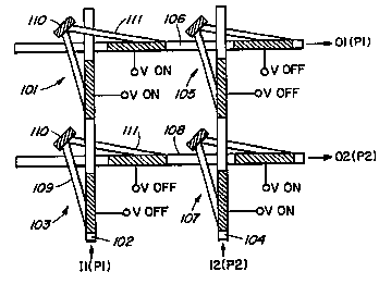
FIGURE 6 illustrates a variation on the
configuration of FIGURE 3 and is similar to the embodiment
of FIGURE 4. In this case the coupling is by way of Y-
branch waveguides 101,103,105 and 107 in both the input .
waveguides 102,104 and output waveguides 106,108. As is
known the index of refraction of Y-branch waveguides can be
controlled by electro-optic, free carrier or thermal
effects. In -turn, the index of refraction can be used to
determine whether the optical signal propagates through the
input waveguide or whether it is directed into the branch
guide. The signal which is deflected into the branch guide'
109 is reflected by the etched mirror 110 and redirected
into the complementary Y-branch guide 111 and hence into the
output waveguide 106,108. The structure shown in FIGURE 6
is intended for a strictly non-blocking application in as
much as only one coupler in an input waveguide is turned on
at any given instant in time. Although not shown in the
figures it is to be understood that a full broadcast cross-
point switch may be constructed using Y-branch waveguides
with proportional voltage control.
The cross-point switch of the present invention
can also be fabricated using vertically coupled directional
couplers. FIGURE 7A shows in a perspective view a normally
'off' digital optical switch. In this structure light in
one or the other waveguide continues to flow in that
waveguide until caused to be coupled into the other
waveguide by a current or voltage bias applied to the
electrode. In FIGURE 7A and in the following illustrations
the optical signal is normally in the lower waveguide 120
unless 'switched' to the top waveguide 122. Although this
is the preferred arrangement, the invention is not limited
to such a structure.
FIGURE 7B shows the light path when a voltage or
current is applied to the electrode 124 so as to turn 'on'
CA 02207175 1997-06-OS
WO 96/18131 PCT/CA95/00665
the coupler. Under these conditions the optical signal is
coupled to the upper waveguide 122 and it will continue to
- propagate therethrough, for digital applications or, if
analog, switched back to the lower waveguide 120. A plot of
5 relative power in waveguide 122 as a functiori of bias
voltage is shown in FIGURE 7C. In this example a bias of
approximately -3.5V causes virtually all of the signal to be
coupled into the upper waveguide 122. Hence, it can be seen
that by switching the bias voltage between 0 and -3.5V, it
10 is possible in effect to create a digital switch.
The effect shown in FIGURES 7A to 7C will now be
described in relation to a cross-point switch with reference
to FIGURES 8 and 9. In FIGURES 8 and 9 a 1x2 switch is
15 illustrated although it is to be understood that an 16x16
switch is contemplated by the invention. As shown in FIGURE
8 the optical signal is launched into the lower waveguide
through which it propagates until in the vicinity of the
first directional coupler 126. As this coupler is in an
'on' mode, the signal is coupled into the upper waveguide
122. The reflecting mirror 128 in the upper waveguide 122
directs the signal into the complementary arm of the upper
waveguide. The directional coupler 130 associated with the
complementary arm is also in an 'on' mode and hence the
signal is coupled back into the lower guide 120 and is
delivered to 132 output. Since substantially all of the
input signal is coupled to the upper guide by the
directional coupler there is no output at 134. As
previously discussed the corner mirrors shown in these
figures are etched down and close to the top of the lower
waveguide.
FIGURE 9 relates to the situation in which the
directional coupler associated with output 132 is off while'
the coupler associated with output waveguide 134 is in an
'on' mode. Again, the optical input signal is launched into
the lower waveguide 120. As the first directional coupler
CA 02207175 1997-06-OS
WO 96/18131 PCT/CA95/00665
16
126 is off there is no coupling of the signal to the
associated upper waveguide and the complete signal
propagates through to the vicinity of the second directional
coupler 127. Since the second directional coupler 127 is in
an 'on' mode the optical signal is coupled to the upper
waveguide where it is reflected at right angles by the
mirror 129. The directional coupler in the complementary
arm is also 'on' which couples the signal back to the lower
guide 120 where it is output at 134. As indicated
previously this concept is applicable in cross-point
switches employing a larger number of input and output
waveguides, for example, an 8x8 matrix. A particularly
advantageous property of this structure is that the
reflecting mirror associated with the upper waveguide can be
located more or less centrally so that it can be used to
reflect signals orthoganally. This is shown in greater
detail in FIGURE 10 which is a top view of the mirror
section. Thus with reference to FIGURE 10, the portion 140
of waveguide 142 to the left of the waveguide 144 can be
used as a second input waveguide. The directional coupler
(not shown) on this arm is independently controllable so
that a signal launched in this waveguide can be coupled into
the upper waveguide for reflection by the mirror 146 i'_
suitably located in the structure. This reflected signal
can be subsequently coupled back down into the lower
waveguide by a directional coupler (not shown) on the guide
14$. Thus this waveguide becomes one of a different set of
output waveguides. Hence a signal in waveguide 140 can be
reflected to waveguide 148 by surface 145 of mirror.146
while at the same time a signal on guide 144 can be
reflected to guide 142 by surface 147 of mirror 146. This
concept will be discussed later in connection with the
implementation of an 8x8 matrix in a 16x16 application.
The foregoing description of a vertically coupled
directional coupler refers to a strictly non-blocking
configuration. The structure is also applicable in ar.
CA 02207175 1997-06-OS
WO 96118131 PCT/CA95/00665
17
broadcast system and this is shown schematically in FIGURE
11A. Each directional coupler 150 is capable of splitting
the optical power of the input signal proportionally so that
an equal power level is delivered to each output waveguide.
In FIGURE 11A a 4x4 switch is depicted and hence each
coupler transfers 25% of the total input power into each of
the four output waveguides. This power splitting ratio is,
of course, dependent on the number of elements in the cross-
point matrix_ FIGURE 11B graphically indicates the relative
bias voltage applied to each directional coupler in order to
obtain the four equal output power components.
A significant aspect of the cross-point switch
structure of the present invention is the possibility of
incorporating optical amplifiers in the active branch guides
of the optical couplers. The optical amplifiers can be used
to compensate for coupling losses, propagation losses as
well as loss due to incomplete reflection at the mirror
surfaces. Further, an optical amplifier when in an 'off'
mode is a good optical absorber. Therefore, all the light
being coupled to the 'off' branch amplifier can be totally
absorbed. This results in a considerable reduction in
inter-channel cross-talk. FIGURE 12A illustrates a
laterally coupled 2x2 cross-point switch with optical
amplifiers in the branch arm 162 of the Y-branch waveguides.
It is to be understood, of course, that the optical
amplifier can be incorporated in either waveguide of the
vertically coupled structure previously discussed. Other
alternatives not illustrated include incorporating the
optical amplifier in branch arm 164 or in the input feed-
guide 166.
In certain applications,it will be necessary to
detect the output with a detector in order to provide an
electrical signal. This can be accomplished by integrating
a photodetector monolithically at the ends of the output
waveguides. FIGURE 12B illustrates a 2x2 cross-point switch
CA 02207175 1997-06-OS
WO 96/18131 PCT/CA95/00665
18
having optical amplifier 160 in branch arm 162 and
photodetector 168 in output waveguides 170,172. In FIGURE
12B separate electrodes are provided at each corner so as to
independently control the operation of the input and output
Y-branch waveguides.
As set out hereinbefore, it is an object of the
present invention to provide an optical cross-point switch
capable of processing 16 input channels into 16 output
channels. The manner in which this is achieved by the
invention is illustrated schematically in FIGURE 13. In a
preferred embodiment the configuration of each cross-point
is based on the structure shown in FIGURES 8,' 9 and 10, that
is, vertically coupled directional couplers with a 45°
mirror to establish the right angled reflection. In this
configuration the input signals are launched into the lower
waveguide with the active branch of the directional coupler
being in the upper waveguide. Upon execution of the cross-
over the signal is returned to the lower waveguide for
delivery of the signal to the output receiver. In order to
achieve the effective 16x16 cross-point switch utilizing an
8x8 matrix it is necessary for the reflecting mirror at each
intersection to be capable of processing two input signals
as previously discussed. As shown in FIGURE 13, input lines
~.1 to 7~.8 are via the rows at the left hand side of the
matrix. The outputs ~.1 - 7~.8 are via the columns at the top
of the matrix. Similarly the input lines ~.9 - x.16 are via
the columns at the bottom of the matrix while the resulting
outputs ~,9-x,16 are via the rows at the right hand side. The
arrangement of turned 'on' directional couplers in FIGURE 13
has been selected to show how all 16 inputs can be switched
utilizing the double mirror concept. Other arrangements '
are, of course, possible for a rearrangeable non-blocking
switch. Similarly a different arrangement will be used in a
broadcast mode.
CA 02207175 1997-06-OS
WO 96/18131 PCT/CA95/0~665
19
FIGURE 14 represents a 16x16 switch in an ATM.
Each of the inputs I1-I16 of FIGURE 14 is capable of
containing multiple wavelength channels, say, for example,
each contains eight different wavelength channels wherein
each wavelength channel has a bit rate of 10 Gb/s. By
combining a 16x16 switch with optical tunable filters which
are capable of processing eight wavelength channels, the
combined switching rate is 1.28 Terabits/sec. This is, of
course, an example only and is not intended to limit the
invention.
In a preferred embodiment the cross-point switch
is fabricated within a chip dimension of 5mm x 5mm utilizing
current wafer fabrication technology. A particularly
suitable material is a III-V compound alloy/substrate such
as GaAs or InP based material systems. It is also within
the scope of the invention to use a silicon substrate or in
fact a polymer material, glass or silica. Other materials
include Site alloy, photorefractive materials such as LiNb03,
and II-VI compound alloys.
The directional couplers and the Y-branch guides
can be designed as either analog or digital switches. The
analog switch is based on the two-mode interference which
can be made in short device length but is sensitive to
wavelength change, polarization state and fabrication
variations. The digital switch is based on only adabatical
one mode evolution which is less sensitive to polarization
state as well as wavelength and fabrication variations but
which requires a longer device length.
while particular embodiments of the invention have
been discussed and illustrated it will be apparent to one
skilled in the art that modifications to these embodiments
or alternative embodiments are possible. For example, 1xN
or Nx1 switch matrices are contemplated by the invention.
The switch can be controlled by locally induced thermal
CA 02207175 1997-06-OS
WO 96118131 PCTICA95/00665
optic effect. It is to be understood, however, that such
modifications and alternatives are within the scope of the
present invention as defined by the appended claims. .