Note: Descriptions are shown in the official language in which they were submitted.
CA 02208178 1997-06-18
L 8955 B
CEB:Ish
FOR
MAGNETIC SWITCH FOR COAXIAL TRANSMISSION LINES
by
Victor H. NELSON
BACKGROUND OF THE INVENTION
The present invention relates generally to switches used for coaxial radio
frequency transmission lines and more particularly to an improved magnetic
switch for use
with such transmission lines.
The prior art related to switches for the control of radio frequency and high
frequency transmission between signal input and signal output transmission
lines have
employed various mechanical devices including: spring actuated contacts,
plungers,
articulated joints arn~ other movable elements to perform the switching
action. These
devices are subject to numerous deficiencies including: poor reliability, slow
response time,
to lack of latching capability and relatively large insertion losses.
The prior art also includes US Patent 4 965 542 which incorporates a cavity
in which one or more conductive contact members are movable from an open
position,
spaced away from pairs of line terminals to a closed position, bridging onr or
more pairs of
terminals. The conta~ members include magnetized strips or non-magnetic strips
carrying
15 magnets or magnetic; members.
CA 02208178 1997-06-18
Despite the advances in the state of the art provided by the switches
according to US Patent 4 965 542, there still remains a need for a coaxial
switch which can
accomplish the switcling function without resorting to multiple solenoids. As
an example,
a single pole, triple throw, SP3T switch would typically require three
solenoids, one for each
2 o position. This results in a switch which is relatively large in size,
expensive, cumbersome,
inefficient and unreliable.
OBJECTS AND SUMMARY OF THE INVENTION
It is an object of the present invention to provide a magnetic switch for
coaxial
transmission lines which is relatively small in size and all switching is
performed in a closed
2 5 Cavity.
Another object of the present invention is to provide a magnetic switch for
coaxial transmission lines which is capable of reliable operation for extended
periods of
time.
Another object of the present invention is to provide a magnetic switch for
3 o coaxial transmission lines which can perform switching operations between
various switch
positions in a random or non-sequential manner.
AnothE~r object of the present invention is to provide a magnetic switch for
coaxial transmission lines which can be configured to provide a range of
switch
configurations.
- 2 -
CA 02208178 1997-06-18
Yet another obj ect of the present invention is to provide
a magnetic switch for coaxial transmission lines which comprises a
relatively small number of component parts resulting in wa
relatively low overall cost.
The foregoing and other objects and advantages of the
present invention will appear more fully hereinafter.
In accordance with the present invention, there is
provided a magnetic switch for coaxial transmission lines which
includes a radio frequency (RF) sub-assembly and an
actuator/indicat:or sub-assembly. The RF sub-assembly has a housing
which includes ;~ fully sealed cavity which is completely sealed
against electro~-magnetic-interference (EMI) where the switching
elements, when selected, move a relatively small distance as part
of the switching action under the influence of magnetic attraction
or repulsion. Typically, four SMA-type or TNC-type or type N radio .
frequency connectors are mounted on the housing and project into
the cavity. Z'he connectors provide gold-plated fixed radio
frequency contacts.
The housing includes four switching paths, each of which
is precision machined to produce a 50 ohm line for the switching
element. Each path contains one of the four switching elements.
The switching elements are preferably made of soft magnetic iron
and are gold plated.
Beneath each of the switching elements, and located
within the housir,,g of the SMA-type or TNC-type connectors, there is
mounted a rare e2.rth magnet that attracts the switching element to
- 3 -
CA 02208178 1997-06-18
its pair of RF c:ontacts. Each of the switching elements includes
a pair of dielectric posts such as tetrafluoroethylene (sold by
duPont under a trademark TEFLON), or equivalents, which project
from the switching element and are slidably mounted in the housing.
The RF sub-asseribly also includes a top ground plate.
The actuator/indicator sub-assembly includes external
attracting magnets which are mounted on a sector motor actuator
- above the switching elements. During operation, the unselected
paths will have f~heir switching elements grounded out by the action
of the external magnets which attract the switching elements to the
ground plate with a relatively strong magnetic force which
overcomes the wE,aker magnetic force of the rare earth magnets in
the RF connector housings.
As a result of the construction of the apparatus of the
present invention, a high degree of electrical isolation is
achieved by grounding the unselected switching elements with
relatively strong magnetic forces in paths that are designed to be
well below electrical cut-off frequencies and by locating the
switching elements in a sealed RF cavity.
BRIEF DESCRIPTION OF TH8 DRAWIN(38
Other important objects and advantages of the present
invention will be apparent from the following detailed description,
taken in conjunc'~ion with an accompanying drawings in which:
Fig. 1 is a cross-sectional view of a magnetic switch for
coaxial transmis:~ion lines according to the present invention:
- 4 -
CA 02208178 2001-02-09
Fig. 2 is a bottom view of the switch of Fig. 1 taken
along line 2-2 in Fig. 1:
Fig. 3 is a fragmentary cross-sectional view, similar to
Fig. 1, showing a switch element contacting a pair of radio
s frequency connectors;
Fig. 4 is a fragmentary cross-sectional view similar to
Fig. 2, but showing the switch element in contact with the ground
plane;
Fig. 5 is a cross-sectional view taken along line 5-5 of
Fig. 1;
Fig. 6 is a cross-sectional view of an alternative
embodiment of the switch of Fig. 1:
Fig. 7 is a bottom view of the switch of Fig. 6, taken
along line 7-7 in Fig. 6;
Fig. 7A is a bottom view of the switch of Fig. 6, similar
to Fig. 7, with a portion shown broken away to reveal details of
the internal construction of the RF cavity;
Figs. 8A, 8B and 8C are schematic diagrams of the various
positions of the switch elements of the embodiment of Fig. 6;
Figs. 9A and 9B are schematic diagrams of the switch
elements of the switch shown in Fig. 1 with the switch configured
as a single-pole-double-throw type of switch;
- 5 -
CA 02208178 1997-06-18
Figs. 10A and lOB are schematic diagrams of the switch
elements of the switch shown in Fig. 1, with the switch configured
as a double-pole-double-throw type of switch:
Figs. ilA, 11B and 11C are schematic diagrams of the
switch elements of the switch shown in Fig. 1 with the switch
configured as a single-pole-triple-throw type of switch:
Figs. 12A, 12B and 12C are schematic diagrams of the
switch elements of the switch shown in Fig. 1 with the switch
configured as a T-type of switch; and
1o Figs. 13A, 13B and 13C are schematic diagrams of the
switch elements of the switch shown in Fig. 5, with the switch
configured as a double-pole-triple-throw type of switch.
DETAILED DESCRIPTION OF THE INVENTION
With reference to the drawings, wherein like reference.
numbers designate like or corresponding parts throughout, ther~ is
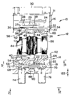
shown in Fig. 1 a magnetic switch for coaxial transmission lines 10
which includes: an actuator/indicator sub-assembly 12 and a radio
frequency (RF) head sub-assembly i4.
The ac~uator/indicator sub-assembly 12 includes: a top
housing 16 and a bottom housing 18 which are connected by support
posts 58, 6o which are typically disposed at the surfaces 20, 22 of
the top and bottc~m housings 16, 18. The top housing 16 includes a
cavity 24 within which there is mounted a reed magnet 26 and a
printed circuit k~oard 27 on which a reed switch 28 and a plurality
of diodes 29 are mounted. Reed switch 28 and reed magnet 26 shown
- 6 -
CA 02208178 1997-06-18
in Fig. 1 are typical of up to three similarly symmetrically
mounted reed switches, one reed switch for each actuation position.
A power connector 30 is mounted on an upper portion 31 of the tbp '
housing 16. Conventional power terminals, which are not shown, may
be used in lieu of the power conductor 30. Lower portion 32 of the
top housing 16 includes a support plate 34, the central portion 36
of which supports the upper end 38 of a shaft 40.
Lower end 42 of the shaft 40 is supported by the bottom
housing 18. A s~:ationary armature 44 is mounted on central portion
46 of shaft 40.
An upF~er bearing 48 is mounted on shaft 40 proximate to
top housing 16 and a lower beariBg 50 is mounted on shaft 40
proximate to bottom housing 18. The upper bearing 48 supports an
upper retainer °_~2 and lower bearing 50 supports a lower retainer
54. The upper and lower retainers 5Z, 54 are connected by a magnet
housing 56 which is capable of rotation relative to the stationary
armature 44 in the order of 90 degrees in a manner which will be
presently described. Top and bottom housings 16, i8 are joined by
the support posts 58, 60 and by a cover 62.
Bottom housing 18 includes magnets 64, 66 which, during
operation of switch 10 are used to attract and ground out selected
switching elemen~~s 68 which are located in a sealed radio frequency
cavity 70 which .is located in a lower portion 72 of bottom housing
18. The contacts i, 2, 3, 4 of the four SMA-type connectors 94,
76, 78, 80, shown in Fig. 2, project into the radio frequency
CA 02208178 1997-06-18
cavity 70. The bottom housing 18 typically includes four switch
elements 68, 82, 84, 86 which are shown in Fig. 10A.
In the various schematic drawings, Figs. 8A, 8H through
12A, 12B and 12C, the switch elements which have been activated and
which are thus ~.n contact with the various contacts 1, 2, 3, 4 are
shown in solid :lines while the switch elements which are inactive
and which have been grounded are shown in broken lines. The
connector contacas of the connectors 74, 76, 78, 80 are indicated
typically by rei~erence numbers i, 2, 3, 4. In Figs. 13A, 13B and
13C, the contacts are indicated by reference numbers 1, 2, 3, 4, S
and the inactivE, switch elements have not been shown for purposes
of clarity of iJ.lustration. The activation of the various switch
elements will bE~ described presently.
As is shown in Figs. 1, 3 and 4, a bottom magnet 88 which
is mounted in the lower portion 90 of the bottom housing 18.
attracts the switching element 68 to the contacts 1, 2 of the SMA-
type connectors 74, 76, thereby completing a radio frequency
circuit between the two SMA-type connectors 74, 76.
As is shown in Fig. 5, the bottom retainer 54 is capable
of rotation in the order of 90 degrees as indicated by the arrows
55 and the rotational travel of bottom retainer 54 is limited by
stops 92, 94, wh:~ch are formed in ground plate 96, which forms th~
upper portion 98 of the radio frequency cavity 70.
Fig. 4 shows how rotation of the bottom retainer 54 into
the position shorn has brought upper magnet 64 into alignment with
switch element 6t;. As is shown in Fig. 4, the upper magnet 64 has
_ g _
CA 02208178 1997-06-18
overcome the attractive force of the lower magnet 88 and has lifted
the switch element 68 away from the contacts 1, 2 and has brought
the switch element 68 into contact with the ground plate 96.
The switch elements 68, 78, 80, 82 are preferably made of
soft magnetic iron. The magnetic force exerted by the upper magnet
64 is preferable in the order of 4 oz . while the magnetic force
exerted by the k>ottom magnet 88 is in the order of 1 oz. so that
the upper magnet 64 easily and reliably overcomes the force of the
bottom magnet 88 when the upper magnet 64 is moved into alignment
with the switch element 68. The bottom magnet 88 is preferably a
rare earth magnet.
The switch element 68 has .a pair of projecting posts 100,
102 which are slidably mounted in holes 104, 106 formed in the .
bottom housing Ls. The posts 100, 102 are preferably made of
Teflon or Kel-F rind have a preferred diameter in the order of 0.062.
inches.
As is :shown in Fig. 10A, each of the switch elements 68,
82, 84, 86 is mountedly guided within a precision-machined path or
slot 110, 112, 1.14, 116, 118 in the housing 18. The paths 110,
112, 114, 116, 118 are proportioned to provide a 50 ohm line for
the switching elements 68, 82, 84, 86. The vertical motion in the
direction shown by the arrow 122 in Fig. 1 is in the order of 0.040
inches, which mail be varied dependent on requirements.
During operation, when a command is received via the
connector 30, the actuator 12 will rotate clockwise or counter-
clockwise to the desired position which is defined by stops 92, 94
_ g
CA 02208178 1997-06-18
as is shown in rig. 5. The selected switching element will come
under the influence of the bottom magnets 88 to be forced into
contact with the contacts 1, 2, 3, 4 to complete the circuit. The
unselected switch elements will be attracted by the top magnets 64,
66 on the actuator 12 and will be forced against the ground plate
96. ,
A unique mechanical advantage is achieved by the switch
according to the present invention in that the actuator 12 does
not require additional prime power to produce increased contact
10 force since all the actuator 12 has to do is position the strong
top magnets 64, 66 over switch elements 68, 82, 84, 86 to produce
the switching action. The contact force is thus solely dependent
on the magnetic forces.
In addition, the switch 10 according to the present
invention: provides a strong and predictable contact force, uses.
a simple highly reliable mechanism which does not rely on plungers,
springs or friction; uses a relatively limited and controlled
movement of the :witching elements 68, 82, 84, 86 . The movement ~of
the switching elements 68, 82, 84, 86 within a defined slot 110,
112, 114, 116 wh=.ch is formed inside a sealed radio-frequency (RF)
cavity 70 resulta in unsurpassed RF performance as measured by
Voltage Standing Wave Ratio (VSWR) and loss performance.
If the upper magnets 66 and 68 are made to attract the
lower magnets 88, a self-detenting action occurs. If magnets 66,
68 are reversed, a self-repelling action occurs. If upper magnet
66 attracts and upper magnet 68 repels, the assembly provides no
- 10 -
CA 02208178 1997-06-18
interaction other than moving the switching elements. The RF sub-
assembly 14 whi~-h includes the RF cavity 70 and the connectors ~4,
76, 78, 80, forms a modular sub-assembly which facilitates testing
at the sub-assembly level prior to assembly with the next assembly.
The reed magnet 26 and the reed switch 28 enable the
actuator/indicai~or assembly 12 to provide a signal which indicates
the rotational position which has been attained by the magnet
housing 56 therE~by providing a feedback signal.
Figs. l0A and lOB show a schematic diagram of the switch
10 of Fig. 1. hs shown in Fig. 10A, switch elements 68, 84 shown
in solid lines, have been selected. Switch element 68 is attracted
to contacts 1, :~ and provides a connection between contacts 1, 2
and switch element 84 is attracted to the contacts 3, 4 and
provides a connection between contacts 3, 4.
Switct; elements 82, 86, shown in broken lines, have been
attracted by magnets 64, 66 and have been grounded by contact with
ground plane or ground plate 96.
In Fig. 10B, in position number two, switch elements 82,
86, shown in solid lines, have been attracted to contacts 2, 3 and
1, 4 while switch elements 68, 84, shown in broken lines, have been
attracted to the ground plane 96. The switch 10 as shown in Figs.
l0A and lOB thus functions as a double-pole-double-throw switch.
Figs. 9A and 9B show the schematic diagram of an
alternative embodiment 200 of the switch 10 of Fig. 1, which
functions as a single-pole-double-throw switch and which generally
incorporates the same structure as Fig. 1 with the exception that
- 11 -
CA 02208178 1997-06-18
three connector: and three contacts 1, 2, 3 and two switch elements
202, 204 are utilized.
Following the same general convention as described in
connection with Figs. l0A and lOB, in Fig. 9A, in position number
one, contacts i and 2 are connected by switch element 202 while in
Fig. 9B, in position number two, contacts 2, 3 are connected by
switch element ;'04.
AnothE~r alternative embodiment of the present invention
300 is shown in Figs. 6, 7, 7A, 8A, 8B and 8C. As previously
described, in connection with Fig. l, the sector motor armature 302
in the actuator assembly 303 remains stationary. Sector motor 304
contains four electromagnetic poles that will react to a rotary
permanent magnet: field.
Armature 302 which is hard-wired, in the order of 60-300
ohms per pole (depending on available voltage), and per RF
position, will receive switching commands producing a magnetic pole
action which wi).1 repel the adjacent stator permanent magnet 306
thereby producing sufficient torque to rotate stator 308 to the
selected position. Magnet housing assembly 310 is supported by a
shaft 311 and bearings 312, 314 in a manner similar to that which
has been previously described.
Stator 308 is maintained in the end positions against a
pair of hard stops 309 by magnetic forces in the sector motor 304
and by attractive forces in the RF head sub-assembly 316, which
will be presently described. Stops 309 in the switch 300 are
similar to stops 92, 94 which have been described in connection
- 12 -
CA 02208178 1997-06-18
with Fig. 5. Reed magnets 319 and reed switches 321 are similar to
like items 26, a8 in Fig. 1 and provide a feedback signal.
As is shown in Figs. 7, 7A and 8A, switch 300 includes
four connectors 318, 320, 322, 324 and five switching paths 326,
328, 330, 332, 334. The connectors 318, 320, 322, 324 are
assembled and hE~ld in place by hexnuts 335.
The fpve switching paths 326, 328, 330, 332, 334 within
. the cavity 315 i_n RF head 316 are precision-machined to produce a
50 ohm line for the switching elements 336, 338, 340, 342, 344. In
i0 contrast to the switching elements 68, 82, 84, 86 previously
described, the switching elements 336, 338, 340, 342 are made of
half-hard brass which has been gold plated. A magnet 346, 348,.
350, 352, 354 is attached to each switching element 336, 338, 340,
342, 344 as is best shown in Figs. 6 and 7A. Switch element
magnets 346, 348, 350, 352, 354 are preferably rare earth type.
magnets and are typically in the order of 2 mm in diameter by 1 mm
in height.
Switch element magnets 346, 348, 350, 352, 354 react to
actuating magnei~s 356, 358 which are mounted on the rotating
housing 360 in a manner which will be presently described. The
size and spacing of the actuating magnets 356, 358 and the switch
element magnets 346, 348, 350, 352, 354 is such that, when
selected, switch elements are repelled by the actuating magnets
356, 358 and are thereby maintained in contact with the contacts 1,
2, 3, 4 by a force which is in the order of one ounce.
- 13 -
CA 02208178 1997-06-18
The sealed RF head 3i6 contains a top ground plate 362,
the five switch elements 336, 338, 340, 342, 344 and the contacts
i, 2, 3, 4 of the SMA type or TNC connectors 318, 320, 322, 324.
As is best shown in Figs. 7A and 8C, during operation,
the selected switch elements 336, 342 are maintained by external
repelling magnets 356, 358 and the unselected paths will have their
switch elements 338, 340, 344 grounded out by external attracting
magnets 372, 374, 376, 378, 380, 382. The external attracting
magnets 372, 37~t, 376, 378, 380, 382 are mounted on the rotating
i0 housing 360 above the switch elements 336, 338, 340, 342, 344.
As previously described, the attracting magnets 372, 374,
376, 378, 380, x:82 provide a force. which is in the order of four
ounces. High isolation is thus achieved by the combination of the
following: grounding unselected switch elements with the above
described, relatively strong, four ounce force; operation of the'
switch elements 336, 338, 340, 342, 344 within precision machined
paths 326, 328, 330, 332, 334 which are proportioned to be well
below cutoff frequencies: and location of the switch elements 336,
338, 340, 342, 3~t4 and the machined switching paths 326, 328, 330,
332, 334 within the sealed RF cavity 315.
The switch 300 according to the present invention is
capable of accomplishing a random switching sequence wherein a
switch 300 may bE~ switched to any of the switching paths 326, 328,
330, 332, 334 regardless of sequence. When a command is received,
the actuator 303 ;gill rotate clockwise or counterclockwise 45 or 90
degrees to the desired position wherein adjacent positions are
- 14 -
CA 02208178 1997-06-18
separated by 45 degrees and the end positions are separated by 90
degrees. Selected switch elements will come under the influence of
repelling magnets 356, 358 to be forced against the selected
contacts to complete the circuit. The unselected switch elements
will be attracted by the external attracting magnets 372, 374, 376,
378, 380, 382 and will be forced against the ground plane 362.
Figs. 7A and 8C show the location of the repelling 356,
358 and attracting 372, 374, 376, 378, 380, 382 magnets: The
contacts have been designated by reference numbers 1, 2, 3, 4. In
Fig. 8C, attracting magnets 372, 374, 376, 378, 380, 382 have been
shown as open circles and the repelling magnets 356, 358 have been
shown as shaded circles. As is shown in Fig. 8C, switch element
336 is in alignment with repelling magnet 358 and switch element
342 is in alignment with repelling magnet 356. The switch element
336 establishes contact between the contacts 2 and 3 while switch
element 342 establishes contact between contacts 1 and 4.
Switch elements 338, 344, 380, shown in broken lines,
have not been se:Lected and these switch elements are urged against
the ground plane 362 by attracting magnets 372, 374, 376, 378, 380,
382.
Fig. 8~'~ shows contact established between contacts i and
3 by switch elem-~nt 338.
Fig . 813 shows contact establ fished between contacts i and
2 by the switch element 340 and contact established between
contacts 3 and 4 by switch element 344.
- 15 -
CA 02208178 1997-06-18
Figs. 11A, 11B and 11C show the schematic diagram of an
alternative embodiment 400 of the invention, which functions as a
single-pole-triple-throw switch and which generally incorporatgs
the same structure as Fig. 1. In Fig. 11A, the contact 4 which
functions as the input and contact 1 are connected by switch
element 402. IIl Fig. ilB, the contacts 4 and 2 are connected by
the switch element 404-and in Fig. i1C the contacts 4 and 3 are
connected by the switch element 406. In Fig. 11A, the unselected
switch elements 404, 406 have been shown in broken lines.
1o Figs. 12A, 12B and 12C show the schematic diagram of an
alternative embodiment of the invention 500 which functions as a
"T" type of a ..witch and which generally incorporates the same
structure as Fig. 1. In Fig. 12A, contacts i and 2 are connected
by switch element 502 and contacts 3 and 4 are connected by switch
element 504. In Fig. 12B, contacts i and 4 are connected by switch
element 506 and <:ontacts 2, 3 are connected by switch element 508.
In Fig. 12C, coni:acts i, 3 are connected by switch element 510 and
contacts 2 , 4 arE~ connected by switch elements 512 . As is shown in
Fig. 12C, the sw~_tch element 510 bridges over and does not contact
the switch element 512.
Figs. 13A, 13B and 13C show the schematic diagram of
another alternative embodiment of the invention 600 which functions
as a double-pole-triple-throw switch and which incorporates a total
of five contacts 1, 2, 3, 4, 5 with contacts 2 and 4 functioning as
the input contacts. Figs. 13A, 13B and 13C also show, in schematic
form, the location of the various switching elements 602, 604, 606,
- 16 -
CA 02208178 1997-06-18
608 and attracting magnets 610, 612, 614, 616 and repelling magnets
618, 620, 622 of the switch 600. Switch 600 has the same general
construction as has been shown and described in connection with
Fig. 6. The attracting magnets 610, 612, 614, 616 have been
illustrated as open circles while the repelling magnets 618, 620,
622 have been illustrated as shaded circles. The attracting
magnets attract i~he unselected switching elements to a ground plate
362 in the manner which has been previously described.
In Fig. 13A, the rotating housing 310 has rotated to a
position definecl as a minus 90 degrees (-90°) position and the
repelling magnets 618, 620 have forced the switch element 602 to
make contact bei:ween the contacts.i and 2 and have forced the
switch element 6U4 to make contact between the contacts 4 and 5, as
indicated by the broken lines 624, 626 which indicate the alignment
of the repelling magnets 618, 620 with the switch elements 602,
604.
In Fig. 13B, the rotating housing 310 has rotated to a
position defined as a zero degree (0°) position and the repelling
magnets 622, 618 have forced the switch element 602 to make contact
between the contacts 1 and 2 and have forced the switch element 606
to make contact t~etween the contacts 3 and 4, as indicated by the
broken lines 628, 630.
In Fig. 13C, the rotating housing 360 has rotated to a
position defined as plus 45 degrees (+45°) position and the
repelling magnet: 622, 618 have forced the switch element 608 to
make contact between the contacts 2 and 3 and have forced the
- 17 -
CA 02208178 1997-06-18
switch element 604 to make contact between the contacts 4 and 5 as
indicated by the broken lines 632, 634.
The switch 600 thus provides a double-pole-triple-throw
switch which uses only a single actuator, thereby achieving a
significant simplification both in mechanical structure and wiring
and an improvement in reliability over the prior art.
The foregoing specific embodiments of the present
invention, as seat forth in the specification, are for illustrative
purposes only. Various changes and modifications may be made
within the spirit and scope of this invention.
- 18 -