Language selection

Search

Patent 2208620 Summary

Third-party information liability

Some of the information on this Web page has been provided by external sources. The Government of Canada is not responsible for the accuracy, reliability or currency of the information supplied by external sources. Users wishing to rely upon this information should consult directly with the source of the information. Content provided by external sources is not subject to official languages, privacy and accessibility requirements.

Claims and Abstract availability

Any discrepancies in the text and image of the Claims and Abstract are due to differing posting times. Text of the Claims and Abstract are posted:

  • At the time the application is open to public inspection;
  • At the time of issue of the patent (grant).
(12) Patent Application: (11) CA 2208620
(54) English Title: TRANSMISSION OF D-CHANNELS IN TELECOMMUNICATIONS SYSTEMS
(54) French Title: TRANSMISSION D'INFORMATIONS DANS LES CANAUX DES SYSTEMES DE TELECOMMUNICATION
Status: Deemed Abandoned and Beyond the Period of Reinstatement - Pending Response to Notice of Disregarded Communication
Bibliographic Data
(51) International Patent Classification (IPC):
  • H04J 14/08 (2006.01)
  • H04J 3/00 (2006.01)
  • H04J 3/12 (2006.01)
  • H04J 3/16 (2006.01)
  • H04J 3/22 (2006.01)
  • H04N 7/173 (2011.01)
  • H04Q 11/04 (2006.01)
(72) Inventors :
  • BOTTIGLIERI, MICHAEL PHILIP (United States of America)
  • BROLIN, STEPHEN JOSEPH (United States of America)
  • KAHN, DAVID BRUCE (United States of America)
  • MASUCCI, JEFFREY ALLEN (United States of America)
(73) Owners :
  • LUCENT TECHNOLOGIES INC.
(71) Applicants :
  • LUCENT TECHNOLOGIES INC. (United States of America)
(74) Agent: KIRBY EADES GALE BAKER
(74) Associate agent:
(45) Issued:
(22) Filed Date: 1997-06-23
(41) Open to Public Inspection: 1998-01-25
Examination requested: 1997-06-23
Availability of licence: N/A
Dedicated to the Public: N/A
(25) Language of filing: English

Patent Cooperation Treaty (PCT): No

(30) Application Priority Data:
Application No. Country/Territory Date
686,971 (United States of America) 1996-07-25

Abstracts

English Abstract


The invention is a circuit for transmitting digital information which
avoids wasting bandwidth when one channel is transmitted at a slower rate than
another channel. A superframe is set up to include a plurality of multiplexed frames.
At least one of the bursts in each frame is shared by a plurality of customers so that
each customer can transmit a full payload once for each superframe.


French Abstract

L'invention est un circuit de transmission d'informations numériques sans gaspillage de la bande passante quand les informations sont transmises à un débit moins grand dans l'un des canaux. Une supertrame constituée d'une pluralité de trames multiplexées est créée. Au moins l'une des salves de chaque trame est utilisée par plusieurs clients, de sorte que chaque client peut transmettre une charge complète dans chaque supertrame.

Claims

Note: Claims are shown in the official language in which they were submitted.

-5-
The invention claimed is:
1. A circuit for transmitting digital information in multiplexed frames
including bursts at a first data rate where at least one channel includes bursts at a
second data rate which is some fraction of the first data rate comprising:
means for storing information transmitted at the second data rate; and
means for transmitting the stored information at designated bursts only
in every nth frame where n is an integer greater than 1.
2. The circuit according to claim 1 wherein the channel is an integrated
services digital network D channel.
3. The circuit according to claim 1 wherein the first data rate is n times
the second data rate, and n multiplexed frames are transmitted as a superframe.
4. The circuit according to claim 3 wherein n is equal to 4.
5. The circuit according to claim 1 wherein the means for storing the
information comprises a memory buffer.
6. The circuit according to claim 5 wherein the memory has a capacity of
at least 16 bytes.
7. The circuit according to claim 1 wherein the means for transmitting
comprises a controller coupled to a transmitter block and to the means for storing.
8. A system for transmitting digital information in multiplexed frames
including bursts at a first data rate where at least one channel includes bursts at a
second data rate which is some fraction of the first data rate, the system comprising:
means for providing a superframe including a plurality of the
multiplexed frames, each multiplexed frame including at least one burst for
transmitting data at the second data rate; and
means for assigning to said burst the channel from different customers
for each of the multiplexed frames within the superframe.
9. The system according to claim 8 wherein the system is an integrated
services digital network and the channel is a D channel.

-6-
10. The system according to claim 8 wherein the first data rate is n times
the second data rate, and the superframe consists of n multiplexed frames.
11. The system according to claim 10 where n is equal to 4.
12. The system according to claim 8 wherein the means for providing the
superframe and for assigning the bursts comprises a channel group controller.

Description

Note: Descriptions are shown in the official language in which they were submitted.


CA 02208620 1997-06-23
- 1 -
TRANSMISSION OF D-CHANNELS IN TELECOMMUNICATIONS SYSTEMS
Field of the Invention
This invention relates to t~kco~ nic~tions t~ ~crni~sion and in
particular to Integrated Services Digital Network (ISDN) tr~ncmiceion
5 Back~round of the Invention
Integrated Services Digital Nelwulk (ISDN) is a l~twoll~ which
provides voice, data and video info~mation ovcr the same ~ ss~ and ~wi~l~ g
fn~ilities Infonnation is usually lli~n;,~ bcl~. ~n a host digital t~- .ni~ql (HDT)
and the cus~ner in the form of two "B" channels (Bl and B2) and a "D" channel,
10 the B ch~mplc in~1ufling voice and data and the D ch~-ncl including data and
signqling inf(~ tir~r~
Recently p,~,~sed ~t~,."s, such as the Hybrid Fiber Couc (HPC)
system, provide for telephony and cable TV tr~n~migsion) as well as new broadband
services (e.g., swilched digital video), over a single n~,twulk using a combih alio of
15 optical fiber and coaxial cable ~l..~n the host digital te.lllil al and a I~I~U1
interface device (NID) located on the side or n~arby each cu- DJ---V 'S locadon.Upsh~,aln tr~n~missi~n is err~t~ in Time Division Muldple Access (TDMA)
frames of 2 milli~econd duration co"lplisillg a number of bursts. Since the bursts are
usually tr~n~min~d at a rate of at least 64 kb/sec and the D cl~nl~e1g are
20 at 16 kb/sec, bandwidth is wasted. This problem is espe~lly acute in d e u~t~direction (from the CV~Iu~..f r to the HDT) where bandwidth is limit~P~l
Summary of the ~vention
The invention in accor~ce with one aspect is a circuit for ~ l;.-g
digital ir~for~ n in multiplexed frames inrlv~ling bursts at a first data rate where at
25 least onc e~ cl inclu~les bursts at a second data rate which is some fraction of the
first data rate. The circuit includes means for storing infs)rmati~n l~ ilt~d at the
second data rate. The circuit further inclucles means for ~ g the stored
inform~tion at ~lesi~n~ed bursts only in every _th frame where _ is an integer greater
than 1.
In accûrdance with another aspect, the invention is a system for
tr~mitting digital information in m-lltirlPYeA frames il-clu~ g bursts at a first data
rate where at least one channel inl~ludes bursts at a second data ratc which is some
fraction of the first data rate. The system in~ludes means for providing a s..~lL~I,c
including a plurality of the multiplexed frames, each multiplexed frame includin~ at

CA 02208620 1997-06-23
least one bursts for trnsmitting data at the second data ratc. Thc system further
comprises means for q~ssigning to said bursts the chqnnel from dirr.,lenl c~ .e.for each of the multiplexed frames within the ~u~lL~..c.
Brief Description of the Fi~ures
S These and other fedlul.,s of the invention are ~elin~2t~J:l in detail in the
following descripdon. In the drawing:
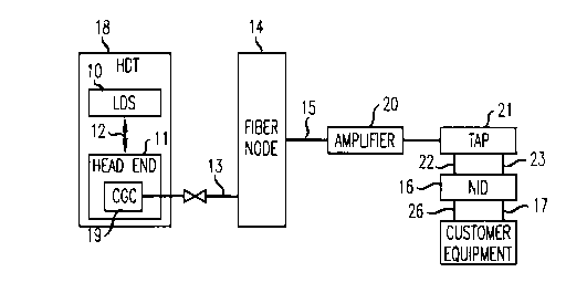
FIG. 1 is a block diagram of a system employing the invention in
accordance with one emb~im~nt;
FIG. 2 is an illustration of a typical m~lltipleYed frame in accordance
10 with the same embodiment;
FIG. 3 is an illustration of a su~lr~ P~ format in acco~-ce with an
embo~liment of the invention; and
FIG. 4 is a block diagram of a circuit for ll-n~ ;ng inf~m~ti~n in the
~u~.rl~ulle format in accordance with the same embo~iim~nt
15 Detailed Description
Referring now to the drawings, in which like iefe~nce numerals
identify similar or identicql cle.--enls, FIG. 1 illu~llat~s a typical hybrid fiber coaY
system which can utili~ the invention.
A Host Digital Terminal (HDT), 18, inel~ldes a Local Digital Switch
20 (LDS), 10, which provides tra~1itirJnql tel&co~ nir~;on~ senices. The LDS is
coupled by means of a bi-directional link, 12, to a Head End, 11, which providesbro~bq-n~ senices such as Cable TV and int~r,q,ctive video. The combined telGph~and bro~b-q-n-l signals are sent out over a bi-directirJn-ql optical fiber link, 13. The
optical fiber link, 13, is coupled to a fiber node, 14, which is located in the vicinity of
25 a plurality of subscribers and typically serves 200 500 subscribers. The fiber node
converts the optical signals to el~c!rir~l signals and l, ~ the e~ ic~l signals
over a coaxial cable, 15.
The coaxial cable, 15, is col rle~ to ~mplifiers, e.g., 20, which can be
used throughout the system to m~int~in co..~ nir~tion~ signal levels and can also
30 be used to split the coaxial signal into several bl~hes. Taps, 21, Sep<udtlE, power
from the commllnir~tion signal, tr~n~ ;ng the communicatir~n signals through a
coaxial cable, 22, and power through a copper pair, 23, to Network Interface Devices
(NIDs), e.g., 16, mounted outside the subscriber's house. A coaxial cable, 17,
connul~ the NlD, 16, to the cust~mer's video e~lu;~ . suCh as a TV or cou ut~r,
35 and one or more pair of copper wires, 26, connr~l to the custQmer's t~k.ph- ne or

CA 02208620 1997-06-23
co ~ ,tf,r rnod~m,
In the reverse direction, electrical signals would be tli ~n~;~t~ from the
u~.er's equipment, through the NID, 16, and the ~...plir,f.~, 20, and to the Sber
node, 14, where the electrical signals would be co~ t,d to optical signals and sent
S baclc to the HDT.
FIG. 2 illustrates the u~ (from NID to HDT) digital trnsmis~;on
format for the system illustrated in FIG. 1. Each TDMA frame, 30, has an interval of
2.0 mi1li-e c and is divided into bursts, e.g., 31, each of which carries ~a~
digital infonnqti~ n from a diff~lenl NID. Each burst, as illustrated, will include a
10 header portion, 32, a payload portion, 33, which carries the messag~ from thec~ ~ r, and a trailer portion, 34. The bursts within a frame may vary in siz~
~penfling upon the type of service provided to each Cu~ ' and ~. h~ lhc~ the burst
is a traffic or control burst. For e~q nple~ the standard voice-grade DS0 service will
have a total of 232 bits with a payload of 128 bits for each B cl~n~ - IIo~
15 within the same 2.0 ms frame, D chq~ lc carry only 32 bits of payload for each
customer with the same o.elhead. Con~e~ e--lly, bandwidth was wasted.
In accordance with a main feature of the in~.enlioll, as illui~t~dt~,d in FIG.
3, a format is provided which involves the creation of four frames, 40, 50, 60, and
70, which cons~ t~ a su~.fi~lle, 80. Each frame of the superframe is similar to the
20 frame, 30, illustrated in FIG. 2, with the excepdon of any bursts, e.g., 41, 51, 61, and
71, which carry D ch-q-nnel infi~rm~ ~i< n Here, four dil're.~. t customers will share the
same posi~i~ (41, 51, 61, 71) ~k~ignq~ for the D channd inrc~l.ladon in the
~lirf~,~. t f~ames, 40, 50, 60, and 70. Thus, frame 40 will carry the infQm~sti~ from
customer Dl in burst 41, frame 50 will carry the D ch ~el ;nr~n... -~;o.- from
25 cUQt~mp~r D2 in burst 51, frame 60 will carry the D ch~ nel inform~ n of c~-t ~ ,r
D3 in burst 61, and frame 70 will carry the D cl~~ ~nel h~ro..-.s~;- n of c~slc~ r D4 in
burst 71. This pattern will be l~at~,d in each subs~,en~ s~pc.L~e. Each
cu~...e-'s D chqrlnel inf~ tion will be delayed for the period of 4 frames so that
each c~Q~J~...e. will transmit the full 128 bit payload when it is his or her turn to use
30 the ~es~ ted positiQn in the ~ Llal..e. Since the D ch~ c are used for data
and si~qling and not for tch~,hon~, the system can tolerate the 8 milli~,c delay from
each cuQtc~me .
FIG. 4 illustrates in some more detail the cilcui~ in each NlD (16 of
FIG. 1) which permits the tr~n~miQsion of the D ch~nl-el infonn~tion as ~escri~
35 above. D ch~nnel information from the c!~tv~"~r is coupled to a memoqy buffer, 83,
which stores the infonnation until it is that .u.to~ ,- 's turn to ~ sll.it in the
&l~p~pliate multiplexed &ame~ In this e~.,ple, where four ~;u t~ are sharing a

CA 02208620 1997-06-23
burst, the memory stores at least 16 Bytes. A controller, 81, which can be a
conven~ nql microcontroller or a high power digital signal p~ss~l, is co.Jp1~d to
the memûry~ 83, and also receives instructions fr~m the Chqnn~l Group Controller(CGC), 19 of FIG. 1, which is located at the Host Digital Tr~ninsl, 18. The CGC
S will inform the con~ller, 81, of the start of each su~r~ lc~ the burst nu...~rwhich is to include the D ch~nnel infnrm~~ion (41, 51, 61, and 71 of FIG. 3), and in
which frame within the ~upc.rl~ c that NID is to ~."..e.~ (40, 50, 60, or 70). The
controller, 81, ll.c.~ folc, releases the stored D chDnnP,I inf~ mD~ n at the app.ul~l;ate
time to the tr~n~mitter block, 82, so that the ih~ro....P~i~n is t~ ~ in the10 ~esign~D~t~ frame.
In general, the invention can be used to L~an ~ bursts from one of _
c~ e.~ in every nth frame where _ is an integer greater than 1.

Representative Drawing
A single figure which represents the drawing illustrating the invention.
Administrative Status

2024-08-01:As part of the Next Generation Patents (NGP) transition, the Canadian Patents Database (CPD) now contains a more detailed Event History, which replicates the Event Log of our new back-office solution.

Please note that "Inactive:" events refers to events no longer in use in our new back-office solution.

For a clearer understanding of the status of the application/patent presented on this page, the site Disclaimer , as well as the definitions for Patent , Event History , Maintenance Fee  and Payment History  should be consulted.

Event History

Description Date
Inactive: IPC from PCS 2022-09-10
Inactive: First IPC from PCS 2022-09-10
Inactive: IPC from PCS 2022-09-10
Inactive: IPC expired 2011-01-01
Inactive: IPC from MCD 2006-03-12
Application Not Reinstated by Deadline 2002-08-26
Inactive: Dead - No reply to s.30(2) Rules requisition 2002-08-26
Deemed Abandoned - Failure to Respond to Maintenance Fee Notice 2002-06-25
Inactive: Abandoned - No reply to s.30(2) Rules requisition 2001-08-27
Inactive: S.30(2) Rules - Examiner requisition 2001-04-25
Application Published (Open to Public Inspection) 1998-01-25
Inactive: IPC assigned 1997-09-25
Classification Modified 1997-09-25
Inactive: First IPC assigned 1997-09-25
Inactive: Filing certificate - RFE (English) 1997-09-05
Filing Requirements Determined Compliant 1997-09-05
Letter Sent 1997-09-05
Application Received - Regular National 1997-09-02
Request for Examination Requirements Determined Compliant 1997-06-23
All Requirements for Examination Determined Compliant 1997-06-23

Abandonment History

Abandonment Date Reason Reinstatement Date
2002-06-25

Maintenance Fee

The last payment was received on 2001-03-23

Note : If the full payment has not been received on or before the date indicated, a further fee may be required which may be one of the following

  • the reinstatement fee;
  • the late payment fee; or
  • additional fee to reverse deemed expiry.

Please refer to the CIPO Patent Fees web page to see all current fee amounts.

Fee History

Fee Type Anniversary Year Due Date Paid Date
Registration of a document 1997-06-23
Request for examination - standard 1997-06-23
Application fee - standard 1997-06-23
MF (application, 2nd anniv.) - standard 02 1999-06-23 1999-03-30
MF (application, 3rd anniv.) - standard 03 2000-06-23 2000-03-29
MF (application, 4th anniv.) - standard 04 2001-06-25 2001-03-23
Owners on Record

Note: Records showing the ownership history in alphabetical order.

Current Owners on Record
LUCENT TECHNOLOGIES INC.
Past Owners on Record
DAVID BRUCE KAHN
JEFFREY ALLEN MASUCCI
MICHAEL PHILIP BOTTIGLIERI
STEPHEN JOSEPH BROLIN
Past Owners that do not appear in the "Owners on Record" listing will appear in other documentation within the application.
Documents

To view selected files, please enter reCAPTCHA code :


To view images, click a link in the Document Description column. To download the documents, select one or more checkboxes in the first column and then click the "Download Selected in PDF format (Zip Archive)" or the "Download Selected as Single PDF" button.

List of published and non-published patent-specific documents on the CPD .

If you have any difficulty accessing content, you can call the Client Service Centre at 1-866-997-1936 or send them an e-mail at CIPO Client Service Centre.


Document
Description 
Date
(yyyy-mm-dd) 
Number of pages   Size of Image (KB) 
Abstract 1997-06-23 1 12
Description 1997-06-23 4 192
Claims 1997-06-23 2 51
Drawings 1997-06-23 2 25
Representative drawing 1998-02-13 1 6
Cover Page 1998-02-13 1 39
Courtesy - Certificate of registration (related document(s)) 1997-09-05 1 118
Filing Certificate (English) 1997-09-05 1 165
Reminder of maintenance fee due 1999-02-24 1 111
Courtesy - Abandonment Letter (R30(2)) 2001-11-05 1 171
Courtesy - Abandonment Letter (Maintenance Fee) 2002-07-23 1 183