Note: Descriptions are shown in the official language in which they were submitted.
CA 02209144 2002-03-O1
Doc. No. 10-44 Patent
Variable Attenuator
Field of the Invention
This invention relates generally to a Bragg grating disposed within a
waveguide and more
particularly, the principal focus of this invention relates to but is not
limited to Bragg grating's
embedded in the core of an optical fibre.
Background of the Invention
to
Various constructions of optical filters are known however so-called Bragg
filters are gaining
popularity. One type of a Bragg filter, which has been developed for sensing
stress and/or
temperature changes in structures is incorporated or embedded in the core of
an optical fiber
by a method disclosed, for instance, in United States patent number 4,807,850.
As is
discussed in this patent permanent periodic gratings of this kind can be
provided or impressed
in the core of an optical fibre by exposing the core through the cladding to
the interference
pattern of two coherent beams of ultraviolet light that are directed against
the optical fibre
symmetrically to a plane normal to the fiber axis. This results in a situation
where the
material of the fiber core has permanent periodic variations in its refractive
index impressed
2o therein by the action of the interfering ultraviolet Light beams thereon,
with the individual
grating elements (i.e. the periodically repetitive regions of the core
exhibiting the same
refractive index behavior) being oriented normal to the fiber axis so as to
constitute the Bragg
gating. The embedded Bragg grating of this Kind reflects the light launched
into the I~iher
core for guided propagation therein, in a propagation direction: only that
lid=I~t having a
?5 wavelength within a very narrow range dependent on the grating element
periodicity is
reflected back along the fibre axis opposite to the original propagation
direction, while being
substantially transparent to light at wavelengths outside the aforementioned
nan-ow band so
that it does not adversely affect the f~rrther° propagation of such
other light. In effect, this type
oi~ aerating creates a ntu~row notch ire floe transmission spectrum, and by
tl~e same tol:cn a
CA 02209144 2002-03-O1
Doc. No. 10-44 Patent
similarly narrow peak in the reflection spectrum. In the applications for
which this kind of
Bragg filter has been developed, any stresses or temperate rre changes
encountered at the
location of the structure in which the Bragg filter is ennbedded affect the
gating and ~hun~~~
its periodicity, or the index of the refraction of the material of the core,
or both so that the
position of the central wavelength in the spectrum is shifted, thus providing
an indication of
tile stress or temperature changes existing or taking place in the structure
being monitored at
the location of the grating. Although the significance of these applications
of Bragg gratings
are formidable, further development in this area is disclosed in United States
patent number
5,007,705 (hereafter refer~r~ed to as the '705 patent) that relates to a
different aspect or use of
to these earlier discovered principles. In the '705 patent various means are
disclosed for
intentionally shifting the reflection wavelength response of a Brag,g grating.
By deliberately
varying the period of the grating or altering the index of refraction in a
predetermined
manner, by external forces or actions on the fibre secticm containing the
<gratin's in a
controlled manner, a variable ligfat filtering element is provi~lcd.
Furthermore, tuning ~r
grating by various means such as the application of heat, compression, or
stretching are all
known.
One useful application of the principals described heretofore, can he found in
United States
patent number 5,446,809 in the name. of Fritz et al. who discloses an optical
fiber wavelength
?0 selective optical switch, utilizing tunable Bragg fibre gratir~g~s. The:
fiber wavelen~,th scle:ctivc
switch has one or more 1 X N input optical couplers and utilizes a plurality
of in-line Bragg
fiber gratings in series along multiple parallel paths. For a given wavelength
of light to pass
through a patrticular grating, the grating must be detuned. By providing a
plurality of Bragg
gratings in series, each designed to reflect a different wavelength, ;end
having means for
?5 controlling or shifting the response of each grating= individually,
si;_>nals can selectively be
passed through a fibre or can be reflected backwards in a binary on-oft
fashion.
Although the prior art describes a plurality of modes and means for varying
the output
response of a Bragg grating within an optical fibre, there remains a need for
useful
CA 02209144 2002-03-O1
Doc. No. 10-44 p~uero
application of this technology that provides a non-binary response. For
example, there
remains a need for a variable attenuator or equalizer that utilizes E~ragg
grating technology.
Therefore, it is an object of this invention to provide an optical equalizer
that incorporates
Bragg gratings.
It is yet a further object of the invention to provide a multi-channel
equalizer.
Summary of the Invention
o
In accordance with the invention, there is provided, an attenuator capable of
controllably
variably attenuating at least two wavelengths of light independently,
comprising: an optical
waveguide section having a plurality of Bragg grating elements disposed
therein in series, at
least two Bragg grating elements having an inclined or sloped reflectivity
response within a
15 predetermined wavelength range that is deter7nined by the periodicity and
rcl~ractive index
variations of the grating elements; and, means for so applyin;~ at least to
c>ne y~ratin'~ ~.I~n~cm
of the optical waveguide section an external influence to modify the
periodicity of the at least
one grating element to shift its central wavelength within a predetermined
wavelength range.
?o In accordance with the invention, there is provided, an attenuator capable
of controllably
attenuating at least two wavelengths of light independently, comprising=:
an optical waveguide section having a plurality of Bragg grating elements
disposed thc;rcin in
series, at least two Bragg grating elements having a sloped reflectivity
response within a
predetermined wavelength range that is determined at least in part by
refractive index
?5 variations of the grating elements;
and means for so applying at least to one grating element of the optical
waveauide section an
external influence to modify a periodicity of the at least one gr~rtinL~
element to shift its
central wavelength within a predetermined wavelength range.
CA 02209144 2002-03-O1
Doc. No. 10-44 Patent
In accordance with the invention, there is further provided, a wave;lengtf~
selective optical
attenuator for attenuating an input signal having a predetermined wavelength,
comprising: an
optical waveguide having an input port and an output port;
at least one optical reflective element located along said optical waveguide
between the input
a port and the output port, said reflecting element reflecting a predetermined
wavelength band
of light centred at a predetermined central wavelength, said central
wavelen~~th being_= at a
base wavelength when said reflective element is not detuned, said base
wavelength including
a predetermined offset corresponding to the predetermined wavelength of said
input signal,
said optical reflective element having a reflectivity along its length that
varies such that one
to end of the grating is substantially more reflective than another end; and,
tuning means,
attached to said reflective element for detuning said central wavelew~th away
from said bsrse
wavelength and towards the wavelength of the input signal so ~zs to attenuate
said
corresponding wavelength of said input signal.
15 Brief Description of the Drawings
Exemplary embodiments of the invention will now be described, in conjunction
with the
drawings, in which:
2o Fig. 1 is a prior art schematic block diagram of an all fiber 2 x 2
wavelength selective optical
switch utilizing tunable Bragg gratings as selective switching elements;
Fi<~. 2a is a schematic block diagram of mufti-channel equalizer in accordance
with an
embodiment of the invention;
?5 Fig. 2b is a schematic block diagram of mufti-channel equalizer including
feedback circuitry
in accordance with an alternative embodiment of the invention;
Fig. 2c is a schematic block diagram of mufti-channel equalizer sirnilar to
that shown in Fie.
2b however including 3 couplets of Bragg grating's;
4
CA 02209144 2002-03-O1
Doc. No. 10-44 Patent
Figs. 3a is a graph showing the amplitude wavelength response of three optical
si~~nals
transmitted into the multi-channel equalizer in an unequalized form, prior to
being
attenuated;
Fig. 3b is a graph showing the reflectivity wavelength response of three Bragg
gratings
corresponding to the circuit of Fig. ?b, including a first wavelengtCn of
whiei~ is shifted, the
=rating being stretched state, a second grating which is unstretched and not
wavelength
shifted, and a third grating which is stretched and wavelength shifl:ed to
achieve substantial
to attenuation of a particular wavelength of light;
Fig. 3c is a graph showing the reflectivity wavelength response of three
couplets of Bragg
gratings, in accordance with the embc>dimenC of the invention that
corresl.aonds to Fig. ?c;
t5 Fig. 4 is a prior art pictorial view showing the bending and stretching of
a Bragg grating non-
uniformly over a bending form;
Detailed Description
?o As was described heretofore, United States patent number 5,446,$09
discloses an
optical switch shown in Fig. 1, wherein Bragg gratings are used as
controllable, selective,
transmissive / reflective binary elements that are capable of transmitting a
predetermined
wavelength of light or alternatively reflecting that wavelength in dependence
upon the period
of the grating. A piezo-electric transducer is coupled to each grating; and
when a particular
?s transducer is energized it stretches the: grating, changing its period, and
thus changes its
reflectivity response by shifting it in wavelength. In this patent the Bragg
gratings operate in a
binary "on-off ' manner to either reflect a particular wavelength of light or
transmit that
wavelength of light.
CA 02209144 2002-03-O1
Doc. No. 10-44 Patent
As described in US 5,446,809 refernng to FIG. 1, an all fiber, wavelength
selective 2 x 2
optical switch has a first optical input signal 10 which travels along an
input port optical fiber
12. The optical signal 10 comprises a plurality of wavelengths ~,, ;>,," ~;,
each wavelen~tlo
acting as an optical chubbier for analog or digital information in a multi-
wavcl~nV~tlz
s communication system. Any number of wavelengths may be used if desired
limited only by
the overall optical bandwidth of the system and individual grating wavelength
width. The
optical fiber 12 is fed to an optical isolator 14 which prevents light from
exiting the input line
12 and disrupting the optical components, e.g., lasers, up-stream from the
input.
The optical signal 10 exits the isolator 14 as indicated by a line 16 to a 1 x
2 optical voupler
(e.g., a 2 x 2 coupler configured as a 1 x 2 coupler in a known way). The
coupler 20
couples a predetermined amount, e.g., 50% or 3 dB, of the input signal 16 to
an output port
22 as a signal 24 on a fiber 26. The remaining portion, e.g., SO~~o, of the
optical signal 16
exits from a port 28 from the coupler 20 as a signal 30 on a fiber 32. Thus,
both output
la signals 24,30 comprise all the wavelengths of the input sranal IO, both
having reduced pc>wer.
e.g., 50~~~.
The optical signal 24 is incident on a first Bragg grating 34 embedded in the
fiber 26. A
Bragg grating, as is known, ret~ects a naz-row wavelength band of light
centered at a reflection
?0 wavelength and passes through all other wavelengths, as described in L1.S.
Pat. T~'o.
4,725,110, "Method for Impressing Gratings within Fiber Optics," co Glenn ct
al.
The grating 34 reflects a narrow wavelength band of light 36 centered at a
wavelength ~,, and
passes all remaining wavelengths as indicated by a line 38. The light 38 is
incident on a
?5 second grating 40 embedded in the fiber 26 which reflects a nan-ow
wavelength band of light
42 c-entered at a reelection wavelength .and passes all remaining wavelengths
as indicated
by a line 44. Similarly, the light 44 travels along the fiber 24 arzd is
incident on a third grating
46 which reflects a narrow wavelength band of light 48 centered at a
reflection wavelength ~,;
and passes all other wavelengths as indicated by a line 50.
6
CA 02209144 2002-03-O1
Doc. Nc~. 10-4~~ 1'ut~nt
Each of the gratings 34,40,46 on the fiber 26 has a piezo-electric tuner (or
PZT) or stretcher
52,54,56 attached to the gratings 34,40,46, respectively. A PZT, as is known,
expands with
applied voltage and is used herein to stretch Bragg grating, thereby tuning
the Bragg gratin's
to a different reflection wavelength or "detuning" the f3ragg grating from its
original
reflection wavelength. The PZT's 52,54,56 are individually controlled by
control lines 57
from a tuner control circuit 58. The control circuit 58 contains known
electronic components
necessary to drive the PZT's and to perform the functions described herein,
and is not critical
to the invention. Also, any other i.ype of stretcher or tuning device,
including a thermal heater,
tU may be used if desired. Some alternative grating tuning devices are
discussed in U.S. Pat. Nc~,
5,007,705, entitled "Variable Optical Fiber Bragg Filter Arrnngcmeat," to
Vlurcy et cil.
The light 36,42,48 reflected by the gratings 34,40,46, respectively, are
collectively indicated
by a line 59 which re-enters the coupler 20 at the port 22 and is coupled to
the input fiber 18
~5 as indicated by a line 60. The signal 60 enters the isolator 14 but does
not exit the isolator l4
on the fiber 12 due to the properties of the isolator which are known.
Similarly, the light
38,44,50 which is passed through the gratings 34,40,46, respectively, are
collectively
indicated by a line 62 which travels along the fiber 24 to an input port 64 of
a 2 x 1 3 dB (or
5U/50) optical coupler 66. The coupler 66 couples a predetermined amount
(e.g., 50°0) of the
?0 light 62 to an output port 68 and onto a fiber 70 as indicated by a line 72
which represents
one of the output lines of the optical switch of the invention. Other
percentages or power'
ratios may be used it desired.
When each of the gratings 34,40,46 are in their unstretched state, i.e.,
having their central
25 reflection wavelength at their base wavelengths ~,,, ~,Z, ~,~,
respectively, the reflected light 59
will comprise all three input wavelengths and the passed signal 62 will not
contain these
wavelengths. Thus, ifthe input signal 10 contains only the wavelengths ~," a."
~," the si~~nal
G? would be 0 or dark. However, when the PZT 52 stretches the orating 34 such
that the
reflection wavelength shifts from ~,, or is "detuned" to some other
wavelength, e.g., ~.,,, as
7
CA 02209144 2002-03-O1
Doc. No. 10-44 Patent
indicated by a line 206 in FIG. 2, the reflection signal 59 will now comprise
only ?~, and i~;,
and the passed signal 62 will now comprise ~,,.
A similar situation occurs if the grating 40 is also "detuned" by the PZT 54
so as to shift the
reflection wavelength 7~z to a different wavelength ~.h, as indicated by a
line 208 in FIG. 2. In
that case, the reflection signal 59 would contain only the wavelength 7~_ and
the; passed signal
62 would comprise the wavelengths ~., and i~~:, n similar situation occurs for
wavelen~~th i_
and the grating 46.
to Thus, by "detuning" any one of the gratings 34,40,46 the passed signal 62
will comprise the
wavelengths of the gratings which have been detuned. Consequently, the
invention in its most
fundamental sense can be viewed as a single input, single output multiple
wavelength
selective switch which allows any one of or any combination of input
wavelengths on floc
input fiber 12 to be coupled to the output fiber 26 based on control lines ~7
from the tuner
15 control circuit 58 which individually control the tuners 52,54,56 attached
to the gratings
34,40,46 along the fiber 26.
A similar arrangement exists for the fiber 32 where a plurality of gratings
X0,82,84 are
embedded along the fiber 32, each having a reflection wavelength n.,, ~~=,
i~;, respectively, and
?o each having a PZT 86,88,90 attached thereto, respectively. Light
collectively reflected from
the gratings 80,82,84 is indicated by a line 92 and light passed by the
gratings 80,82,84 are
indicated collectively by a line 94 along the fiber 32. The fiber 32 is fed to
a first port 96 of a
2 x 1, 3 dB (50/50) optical coupler 98, which couples a Ioredetermined amount,
e.a., 50G1~, of
the light 94 to an output port 100 along the fiber 102 as indicated by a line
104.
In another fundamental configuration of the present invention, a single-input
dual-output,
wavelength selective optical switch is provided at the output signals 62,94
where the outputs
would be the fiber 26 and the fiber 32. This would allow any one of or any
combination of
the input wavelengths 7~,, ~", a~; to be selectively switched to either the
output line ?6 or the
CA 02209144 2002-03-O1
Doc. No. 10-44 Patent
output line 32 or both.
Because many communication systeans allow input signals from different laser
optical
sources, where each source provides common wavelength can -iers, any
communication
switching network must provide for a plurality of inputs, one frorr~ each of
such different
optical source. Consequently, a second input optical fiber 110 carries a
second optical input
112 comprising a plurality of wavelengths, e.g., ~,,', ~,,,', 7~~', these
being the same wavelengths
as those on the first input line 12, however, being from a different source
and thus car7-yin~~
different .information on the can-ier wavelengths. Line ( 10 is feel to are
optical isolator 1 1 ~l
to (similar to the isolator 14) which prevents light from exiting along the
input line 110. The
signal 112 exits the isolator as the optical signal 116 on a fiber 118. The
optical fiber 118 is
fed to an optical 1 x 2 3 dB (50/50) coupler. The coupler 120 couples a
predetermined portion
(e.g., 50%) of the light 116 to an output port 122 as indicated by a line 124
on a fiber 126.
U The light 124 on the fiber 126 is incident on a series of three fiber
gratings 128,130,1 32
impressed in series along the fiber 124. Similar to the gratings on the fibers
26 and 32,
discussed hereinbefore, the gratings I 28,130,132 have central reflection
wavelengths of ~,,, ~,=,
~,;, respectively. Similarly, the gratings 128,130,132 have PZT's 134,136,138
attached thereto
respectively, similar to that discussed for the gratings On the fiber 26 and
32. The light
o reflected by the gratings 128,130,132 is collectively indicated by a line
140 and the light
passed by the gratings 128,130,132 is collectively indicated by a line 142.
Reflected light 140
re-enters the coupler 120 at the port 122 and a portion (e.g., 50%) exits the
coupler onto the
fiber 118 as indicated by a line 144. The light 144 is incident on the
isolator 114 which
prevents the light from exiting the input fiber 112 and disrupting any up-
stream optical
?5 sources.
The fiber 126, along which the passed optical signal 142 travels, is connected
to a second
input port 150 of the coupler 66. The coupler 66 couples a predetermined
amount, e.g., 50%,
of the light 142 to the output port 68 onto the output fiber 70, as indicated
by a line 72.
9
CA 02209144 2002-03-O1
Doc. No. 10-~t4 I';cent
Symmetrically, the coupler 120 couples a predetermined amount, e.g. 50%, of
the light 116 to
an output port 154 as indicated by a line 156 along a fiber 1.58. The light
156 is incident on a
plurality of gratings 160,162,164 imlaressed in the fiber 158 in series in a
similar fashion to
the gratings of the fibers 26,32,126, as discussed hereinbefore. Similarly,
each of the: Lratin~,~s
160,162,164 has a central reflection wavelength 7~,, 7~" ~.3, respectively,
and has a PZ'I"
166,168,170 attached thereto, respectively. The light reflected by t:he
gratings 160,162,164 is
collectively indicated by a line 172, and the light passed by the gratings
160,162,164 is
indicated collectively by a line 174. 'the reflected light 172 re-enters the
coupler 120 at the
t0 port 154 and the coupler 120 couples a predetermined amount (e.~,., 50~% )
of the light 172
onto the fiber 118 as also indicated by the line 144. The light 144 enters the
isolator 114
which prevents such reflected light from exiting along the input line 110 and
disrupting up-
stream sources, as discussed hereinbefore.
t5 The passed light 174 travels along the fiber 158 which is fed to an input
port 176 of the
coupler 98. The coupler 98 couples a predetermined ar~~ount (i.e., 's0~%~) of
the light 17~ to the
output port 100 onto the second output fiber 102 as indicated by the line 104.
Thus the
couplers 66 and 98 act as optical combiners of the signals 62,142 to the
output signal 72 and
of the signals 94,174 to the output signal 104.
~o
The coupler- 120 and the gratings on the fiber's 126,158 operate in precisely
the same fashion
as discussed hereinbefore regarding the coupler 20 and fiber gratings and
PZ'r's attached
thereto on the fibers 26,32. In general, when all the gratings on a given
fiber are not stretched
(or not "detuned"), all the wavelengths of the input signal 112 are reflected
for that fiber.
?5 Similarly, when one of the gratings is "detuned" so as not to reflect at
the unstretched
reflection wavelength for that grating, that wavelength will pass through all
of the series
gratings on that fiber. Additionally, the couplers 66,98 act effectively as
optical combiners. In
particular, the optical coupler 66 combines the optical passed sign~ul 62 from
the gratings
34,40,46 along the fiber 24 and the optical passed signal 142 from the
gratings 128,130,132
CA 02209144 2002-03-O1
Doc. No. 10-44 Patent
on the fiber 126, to the output fiber 70 as the signal 72. This allows any i>f
the wavelengths
on the first input line 12 to be coupled to the output fiber 70 and/or any of
the same
wavelengths on the second input line 110 to be coupled to the output fiber 70,
having a
similar amount of signal loss for both channels.
Similarly, the optical coupler 98 acts as an optical combines to combine the
passed optical
signal 94 from the gratings 80,82,84 along the fiber 32, and the passed signal
174 from the
fiber gratings 160,162,164 along the fiber 158, to be provided along the
second output fiber
102. This allows any of the wavelengths on the first input line 12 to be
coupled to the second
to output line 102, and/or any of the wavelengths on the second input 110 to
be coupled to the
second output fiber 102. Thus, this configuration, which is also known as a
crossbar
configuration in electronic networking, provides an optical crossbar switching
network which
allows any wavelength or combination of wavelengths along any input to be
routed to any
output, in combination with any wavelengths from any other input.
Referring generally now to Figs. 2a to 2c, an equalizer circuit is shown
wherein Bragg
gratings or elements are utilized in a controllable manner to attenuate a
multiplexed input
optical beam comprising three signals of three wavelengths, ?~ 1, ?~2, and
?~3. In the dra~~ in'~~.
the three signals on the left side axe unequal in amplitude, 7~2 having the
least intensity, then
7~1 followed by 7~~i having the highest intensity. In many instances it is
preferred to have the
optical signals equalized, wherein their amplitudes are as close as possible
to one another.
One use of the equalizer of this invention is with rare-earth doped optical
fiber amplifiers.
One limitation of any rare-earth doped optical fibre amplifier is unequal gain
over a
range of frequencies or optical channels of interest, as well as for various
input signal
strengths (i.e. different saturation levels). Over a 35 nanometer gain
bandwidth, erbium
doped fibre amplifiers (EDFAs) typically exhibit a LO to 15 dB small-signal
gain variation. In
long chains of cascaded EDFAs small spectral gain variation can result in
unacceptable large
11
CA 02209144 2002-03-O1
Doc. No. 10-44 Patent
difference in received optical power and therefore, it is preferable to lessen
even small
spectral variation in gain.
To date, several gain equalization and flattening techniques have been
proposed and
described in a variety of prior art references. For example, gain clamping
with enhanced
inhomogeneous saturation is described by V.L. da Silva et al. in an article
entitled,
''Automatic gain flattening in Er-doped-fiber amplifiers," in Proc. OFC'93,
paper THD2,
P.174. 1993. One of the limitations of this method is the re~~uircrr~cnt that
fibre by coolucl to
77 K. The use of passive internallexternal filters has been explored by M.
Tachibana, et al., in
1o an article entitled, "Erbium-Doped Fiber Amplifier With Flattened Gain
Spectrum," in IEEE
Photonics Technol. Lett. 3, no. 2, 118, 1991; by M. Wilkinson, et al., in an
article entitled,
"D-Fibre Filter For Erbium Gain Spectrum Flattening," in Electron. Lett. 28,
no. 2, p. 131,
1992; and by Kashyap, et al" in an article entitled, "Wideband Gain Flattened
Erbium Fibre
Amplifier Using a Photosensitive Fibre Blazed Grating," in Electron. Lett. 29,
no. ?, P.1 ~4,
is 1993, and as well by Grasso et al, in an article entitled, "980-mn diode
pumped Er-doped
fiber optical amplifiers with high gain-bandwidth product," in Proc;. OFC'91,
paper FA3, p.
195, 1991. Another attempt to provide a doped optical fibre amplifier that is
suitable for use
over a range of frequencies is described in U.S. patent ~,?~5,4C7 entitled,
''Amplifier with a
Samarium-erbium Doped Active Fibre," issued Sept~:rnber I~, 1993 in the name
of Grasso et
?0 al. Although the invention described in the patent works well at particular
wavelengths and
for particular signal strengths, it has been found to be limited at other
wavelengths.
However, a major limitation with most of these devices and methods is the
requirement for
bulk optics and non-standard components. The use of external active acousto-
optic filters has
been explored by S.F.Su et al. in an article entitled, "Gain Edualization in
Multiwavelength
~5 Lightwave Systems Using Acoustooptic Tunable Filters," in IEEE Photonics
Technol. l,ett. =f.
no. 3, p.269, 1992; the drawback with this proposal is that it requires bulk
optics, and is
complex in design.
t?
CA 02209144 2002-03-O1
Uoc. No. 10-44 Patent
The exemplary circuit shown in Fig. 2a in conjunction with the responses shown
Figs.
'fib and 3c can be used to offset the unequalized gain over a wavelength
region exhibited from
commercially available erbium doped amplifiers; or, can be used to vary or
offset the relative
strengths of particular wavelengths prior to amplific;.~tion so as to obtain a
relatively
equalized signal after amplification. Although only three Bragg gratings 102,
104, and 106
are shown, other gratings can be included and chained in series tuned to other
wavelengths of
interest.
Referring specifically now to Fig. 2a, a circuit is shown wloerein three
l3ragg gratin~,~s
102, 104, and lOC are shown in series written into an optical fiber 1D1.
Tuning means in the
form of individually controllable piezo-electric transducers 102a, 104a, and
106a are coupled
to the respective gratings each for changing the period of a grating in
dependence upon a
control signal. A tuning control circuit 108 can be preprogrammed. or
programmed in real-
time for issuing appropriate control signals to the transducers. Each of the
Bragg gratinUs
t5 102, 104, and lOG ore designed to have a different period, and are
consequently designed Cc>
affect a different channel. In one embodiment, the gratings are chirped,
appodized gratings
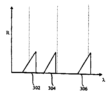
having a sloped or inclined reflectivity response as shown in Fig. 3b.
Therefore the refractive
index difference On between adjacent regions within each of the gratings
varies along the
length of the chirped grating so as to provide a sloped reflectivity response
over a
?0 predetermined wavelength region. Of course, other methods of Forming
rcflective/transmissive elements having a variable reflectively response can
he envisa~~ec(.
One way of fabricating the grating is to provide a standard linear chirp using
a mask; when
exposing the fibre an amplitude mask can be utilized so that one side of the
grating is
exposed more so than the other, resulting in a periodicity that varies in
refractive index rather
''S than in distance, providing a variable masked chirp. The effective An can
be varied by
varying the width of 0n sections. Another means of providing a sloped reunion
is by usin;~ a
very short hydrogen loaded grating, for example one having a ?rim bandwidth,
can be
utilized; by providing such a grating, tuning can be achieved by utilizing the
falling or rising
13
CA 02209144 2002-03-O1
Doc. l~To. 10-~l~l f'at~nt
edge of the gratings reflectivity response. By tuning or wavelength shifting
these gratings a
variable reflectivity response and consequently a variable amount of
attenuation is provided.
Another means of achieving a chirp in a grating is by stretching or bending a
grating having a
non-varying period in non-uniform manner. For example, a grating shown in
prior art Fig. 4
is shown being bent over a form having non-uniform bend radius. By doing so,
the heric.ol ol~
the grating is changed in such a manner as to vary it along its length,
thereby chirping the
grating The authors of this prior art reference, Variable- spectral response
optical waveguide
Bragg grating filters for optical signal processing by K. O. Hill et ;z1.,
Optics Letters / Vol. 20,
No. 12, June 15, 1995 disclose the usefulness of non-uniformly bending a
grating, in relation
1o to signal processing applications, for example for dispersion compensation;
however, we
have found a particularly useful feature that is less related tc.n the
processing of optical signals.
The advantage of such a scheme is as follows; a substantially long grating
with a uniform
period typically has a very narrow reflectivity response; thus, when the
grating is un-bent, it
can be hidden or stored between adjacent channels essentially "tucked away".
In the instance
~5 where an adjacent channel or wavelength range is to be attenuated, the
grating can be bent
and thereby chirped so that range of reflectivity broadens, in a mariner
similar to an opening
curtain. Of course by stretching or compressing the grating its effective
wavclenv~th ran;~e
shifts. Thus the grating response can be compressed, expanded, and/or shifted.
2o Standards and specifications are provided by the telecommunications
industry
regarding the minimum allowable or acceptable channel spacing between two
transmission
channels. In some instances where it is desired to have a plurality of
channels within a small
wavelength region, this spacing labeled G on Fig. 3a, is relatively small. In
order to provide a
grating having reflectivity response that conveniently lies within this space
G in one mode of
?5 operation, and that can be shifted to have a reflectivity response that
coincides with the
wavelength or channel of interest ~,1, ~,2, or 7~3 in a variable manner so as
to attenuate a
particular channel by predetermined amount, the grating must have:
predetermined
characteristics. For example, the grating of interest must be designed to hove
a slope of the
reflectivity response that is suitable for a particular application. Fig. 3c
shows an embodiment
14
CA 02209144 2002-03-O1
Doc. No. 10-44 Patent
wherein grating couplets are provided, each grating of a couplet of gratings,
being tunable
over substantially the same range, and wherein the couplet can share a same
space G for
convenient storage when no attenuation is required. In another embodiment
compressive
actuation means are also or alternatively coupled to each grating, or each
other grating; in this
arrangement one grating of a couplet can be used to attenuate an adjacent
higher wavelength,
while the other gating of a couplet can be utilized to attenuate an adjacent
lower wavelength
signal, by stretching of the gratings and compressing the other of the
gratings a predetermined
amount. It should be noted, that although the gratings shown are preferably
impressed within
an optical fibre, other optical waveguide structures can conveniently be
utilized; for example
to a plurality of gratings can be written into a slab waveguide wherein
heating elements can be
used to control the wavelength reflectivity response of the gratings.
Turning now to Fig. 2b, a circuit is shown for equalizing an input beam of~
li'rht The
circuit is similar in many respects to that of Fig. 2a, however includes a
feedback circuit for
providing information relating to the input beam after it has been attenuated.
A tap, 112 taps,
for example, 5% of the attenuated beam and couples this light to a circuit 116
for further
processing. The tapped light is wavelength dernultiplexed into three channels.
The intensity
of signals representing a 5% portion of wavelengths ~,1, ~,2, and ~,3 are
measured by circuit
116 and converted to electrical signals by photodetectorws (not shown). A
tuner control circuit
114 in response to these electrical signals continuously and dynamically
varies the response
of the gratings 102, 104, and 106 by providing an appropriate voltage to the
actuators 102a,
104a, and 106x. The circuit of Fig. 2c operates in a similar manner, however
the tuner 124
provides appropriate voltages to six I3ragg gratings, 102, 102b, 104, 104b,
106, and 106b.
Of course, numerous other embodiments may be envisaged, without departing from
the spirit
and scope of the invention.
I5