Note: Descriptions are shown in the official language in which they were submitted.
CA 02209225 1997-06-30
WO 96/19025 PCT/US95/16494
-1-
SERIES COMPENSATOR INSERTING REAL AND REACTIVE
IIVVIPEDANCE INTO ELECTRIC POWER SYSTEM
FOR DAMPING POWER OSCILLATIONS
BACKGROUND OF THE INVENTION
Field of the Invention
This invention relates to apparatus for damping power oscillations in
electric power systems. More particularly it relates to a series compensator
which
can insert both real and reactive impedance into a transmission line to dampen
the
power oscillations.
Background Information
Power oscillation frequently occurs in electric power systems due to
disturbances, such as transmission line faults, line and load switchings,
equipment
failures and other events causing rapid system changes. Such power oscillation
has
the undesirable effect of limiting the maximum transmittible power in the
system.
U.S. patent number 5,198,746discloses a solid-state series compensator that
injects
a controllable, 60 Hz voltage in quadrature with the transmission line
current. This
injected voltage has the same compensating effect as that obtained with a
variable
capacitor, or inductor, connected in series with the line. The damping of the
power
oscillation, is achieved by appropriate modulation of the effective 60 Hz
reactive
impedance that the compensator injects in series with the line. That is, when
the
power in the line is increasing, as a result of acceleration of the power
generator
at the "sending-end" of the line and the consequent increase of the
transmission
angle, the capacitive impedance of the compensator is increased by increasing
the
magnitude of the inserted 60 Hz voltage that lags the line current by 90
electrical
degrees, in order to increase the degree of series compensation and thereby
the
CA 02209225 1997-06-30
WO 96/19025 PCT/US95/16494
-2-
transmittable power. Conversely, when the power in the line is decreasing, as
a
result of the deceleration of the "sending-end" generator and the consequent
decrease in the transmission angle, the inserted voltage is made to lead the
line
current in order to create, in effect, an inductive output impedance and
thereby to
increase the overall inductive impedance of the transmission line.
The series compensator of patent number 5,198,746utilizes a do to
ac converter to generate the quadrature voltage. The ac terminals of the
inverter
are connected in series with the transmission line through a coupling
transformer.
A capacitor connected across the do terminals provides the do input voltage
for the
converter. As the converter is theoretically only exchanging reactive power
with
the transmission line, there is no power drain on the capacitor. However,
there are
in reality losses in the switching circuits of the inverter. The real power
needed to
make up for these losses is provided by generating the compensating voltage at
a
phase angle slightly less than 90 ° .
U.S. patent number 5,343,139 discloses a generalized power flow
controller for controlling the flow of power through the transmission line on
a
sustained basis. This power flow controller also utilizes a do to ac inverter
which
injects a voltage in series with the transmission. line voltage. ~ However,
the phase
angle of the injected voltage relative to line current is not limited to
substantially
20. 90° as in the case of the compensator of U.S, patent number.
5,198,746, but is
controllable to any phase angle between 0 and 360 ° . The particular
phase angle
and the magnitude of the injected voltage may be selected to adjust any or all
of
the transmission line effective impedance, the effective phase angle between
voltages at the two ends of the transmission line, and transmission line
voltage
magnitude. This results in the adjustment of both real and reactive line
impedance.
CA 02209225 1997-06-30
WO 96/19025 PCT/US95/16494
-3-
Real power needed to adjust the real component of impedance is provided to the
do to ac converter by an ac to do converter having its ac terminals connected
in
shunt to the transmission line and its do terminals connected to the do
terminals
of the compensator converter through a do link which includes a capacitor. The
response of this flow controller is rapid enough that it can provide dynamic
control
of power flow, and it is also suitable for damping oscillation which may
develop in
the power system. However, this equipment designed primarily for power flow
control, is more complex and expensive than the series compensator described
in
U.S. patent number 5,198,746.
There is a need for improved compensator for damping oscillations
in electrical power systems.
More particularly, there is a need for such an improved compensator
which can provide real power modulation as well as reactive power modulation
to
damp out power system oscillations.
SITM1VIARY OF THE INVENTION
These needs and others are satisfied by the invention which is
directed to enhanced apparatus for providing series compensation to dampen out
oscillation in an electric power transmission line which provides both real
power
and reactive power exchange with the power system. A particular feature of the
invention is that it can provide injection of virtual positive real impedance
in series
with the transmission line to absorb real power as the generator accelerates
during
power oscillations. During those periods of the oscillation when the real
power on
the transmission line decreases, virtual negative real impedance is inserted
in series
with the transmission line to supply real power to the system. The virtual
positive
real impedance can be provided by a resistor which is selectively connected to
absorb real power from the transmission line, and the virtual negative real
impedance, which provides real power, can be provided by an energy storage
device. The energy storage device; such ~as a battery or a super conducting
magnet,
can ~be used to supply both the virtual positive real impedance by absorbing
real
power, and the virtual negative real impedance by supplying real power. The
virtual positive and negative real impedances are injected into the
transmission line
together with reactive compensation. A switching power converter generates a
compensation voltage having y a magnitude and a phase angle relative to
CA 02209225 1997-06-30
WO 96/19025 PCT/US95/16494
-4-
transmission line current which provides the required reactive and virtual
real
impedances. This voltage is injected in series with the transmission line
voltage
through a coupling transformer.
The switching power converter generates both the positive and
negative reactive power required internally. The real power is supplied and
absorbed by power exchange means connected to the do terminals of the
switching
power converter.
It is not necessary that both positive and negative real impedance be
provided, although more precise control can be effected through injection of
both
positive and negative real impedance into the transmission line. The fact that
it
is not necessary in accordance with the invention to inject both positive and
negative real impedance into the transmission line is advantageous because
providing positive impedance is easier and less costly than providing negative
real
impedance.
More particularly, the invention is directed to:
Apparatus for providing series line compensation with enhanced
capability to dampen oscillations in an electric power transmission line
carrying ac
current at a selected transmission line voltage and fundamental frequency,
said
apparatus comprising:
compensation means coupled in series with said transmission
line injecting into said transmission line a compensation voltage at said
fundamental frequency with controllable magnitude and phase angle relative to
said
ac current in said transmission line;
power exchange means selectively connected to said
transmission line only through said compensation means; and
control means controlling the controllable magnitude and
phase angle of said compensation voltage to insert selected reactive and
virtual real
impedance into said transmission line to dampen said oscillations, and
selectively
connecting said power exchange means to said compensation means to enable said
3b compensation means to provide said virtual real impedance.
- BRIEF DESCRIPTION OF THE DRAWINGS
CA 02209225 1997-06-30
WO 96/19025 PCT/US95/16494
-5-
A full understanding of the invention can be gained from the
following description of the preferred embodiments when read in conjunction
with
the accompanying drawings in which:
" Figure 1 is a schematic diagram of a simple power system.
Figure 2 is a plot of electric power transmitted versus transmission
r
angle for the power system shown in Figure 1.
Figure 3A is a schematic diagram of a portion of the power system
of Figure 1 incorporating the present invention.
Figure 3B is a phasor diagram illustrating the compensating voltage
injected in accordance with the invention into the power system shown in
Figure
1.
Figures 4A - 4D illustrate waveforms pertinent to an understanding
of the operation of the invention.
Figure 5 is a schematic diagram of a series compensator for the
electric power system of Figure 1 in accordance with one embodiment of the
invention.
Figure 6 is a schematic diagram of a second embodiment of a series
compensator for damping power oscillations in the electric power system of
Figure
1.
Figure 7 is a schematic diagram of a generalized form of the series
compensator of the invention for damping power oscillations in the electric
power
system of Figure 1.
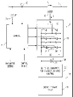
Figure 8 is a block diagram of the series compensator in accordance
with the invention.
Figure 9 is a block diagram of an internal control for the series
compensator of the invention.
Figure 10 is a block diagram illustrating in more detail portions of
the internal control system of Figure 9.
DESCRIPTION OF THE PREFERRED EMBODEVIENT
The subject invention is directed to a novel series compensator for
damping power oscillations in electric power systems. In order to explain the
proposed operation and control of this novel series compensator reference is
made
to the simple power system shown in Figure 1.~ This system 1 consists of a
sending-
CA 02209225 1997-06-30
WO 96119025 PCT/US95/16494
-6-
end generator 3, a transmission line 5, represented by its series inductive
impedance, X, and a receiving-end power system 7 that can be considered as a
power bus of inf'mite capacity. If the voltage phasor at the sending-end of
the
transmission line 5 is s and that at the receiving-end is r, then the
transmitted '
electric power, P~ , can be expressed by the following equation:
Pe= (vs . v,~x~ sin s Eq. (1)
where Vs and Vr are the magnitudes of ys and yT , respectively, and b is the
angle between ys and yr . The power Pe is shown plotted at fixed VS , Vr , and
X
against angle 8 in Figure 2. It can be observed that the maximum transmittable
power is
Pe max=VS. V,JX Eq. (2)
obtained at b = 90 degrees.
In present power systems the power generator 3 is a rotating electro-
magnetic machine that converts the mechanical input power P~ , usually
provided
by a steam or gas turbine 9, into the electric power Pe feeding the
transmission
line 5. Under steady-state operating conditions, the mechanical input power PM
is equal to the electrical output power P~ (neglecting losses), and the
turbine-
generator set 3,9 runs at a constant speed such that a constant transmission
angle
80, necessary to satisfy the Pm=Pe equilibrium, is maintained (see Figure 2).
The
occurrence of power oscillation is due to the fact that, whereas the electric
power Pe
can be changed almost instantaneously in the transmission line (often by
unforeseen and accidental events such as transmission line faults and
equipment
failures), the mechanical input power Pm can be changed only very slowly due
to
a
the nature of mechanical controls and the large inertia involved in the
rotating '
system. Therefore, in the event of a transmission line fault or other
disturbances
. ,
in the electrical power system l, the generator 3 receives more mechanical
input
power than the electric power transmittable by the faulty transmission system.
As
a result, the generator 3 starts to accelerate and the transmission angle
becomes
CA 02209225 1997-06-30
WO 96!19025 PCT/US95/16494
_7_
larger than the steady-state angle 80. The process of acceleration of course
means
that the surplus mechanical energy is being stored mechanically by the
rotating
inertia of the turbine-generator set. In order to re-establish the steady-
state
equilibrium after fault clearing, this stored energy must be absorbed from the
rotating mechanical system. Depending on the overall Q (quality) factor of the
total electro-mechanical system, the absorption of this surplus energy can
take a
number of oscillatory cycles during which the electric power in the
transmission
system may widely fluctuate. In some cases, when the total system has negative
damping, the magnitude of the oscillation keeps increasing until the system
protection shuts-down the disturbed generator.
It is clear that, in principal, the oscillatory energy can be eliminated
from the affected system in two ways. One is by increasing and decreasing the
transmitted power in sympathy with the acceleration and deceleration of the
generator and thus in sympathy with the positive-going and negative-going
swings
of the electric power. The other one is to subtract directly the surplus
energy from
the transmission system when the generator accelerates and dissipate it or
return
it to the system, from a temporary storage, when the generator is in the
declaration
interval.
U.S. patent number 5,198,746 proposes a novel method for the
implementation of only the first approach. That is, the series compensator ,
is
controlled to decrease the transmission line impedance, and thereby increase
the
transmitted power during the acceleration periods of the machine, and to
increase
the transmission line impedance, and thereby decrease the transmitted power
during the deceleration periods. This is accomplished by injecting a voltage
at the
fundamental frequency (60 Hz) into the transmission line in quadrature with
'the
current flowing in the transmission line. The injected voltage lags the
current by
90° for capacitive impedance and leads it by 90° for inductive
impedance. It is
evident that the method of power oscillation damping described in patent
number
5,198,746 is based on a one dimensional modulation of the output of the series
~ compensator. That is, the injected voltage is kept essentially in quadrature
with
respect to the line current so that the power exchange between the series
compensator and the ac system is substantially reactive.
CA 02209225 1997-06-30
WO 96/19025 PCT/US95116494
_g_
Our invention is based on a two dimensional modulation of the
output of a series compensator. That is, the phase angle between the injected
fundamental (60 Hz) voltage and the transmission line current is chosen so as
to
force both reactive and real power exchange between the series compensator and
the ac system. This is illustrated in Figures 3A and 3B. As shown in Figure
3A,
the series compensator 11 injects a compensation voltage V~ into the
transmission
line 5 in series with the line voltage VI through a coupling transformer 12.
Figure
3B is a phasor diagram showing the injected voltage V~, line current IL, and
system
voltage Y~,S phasors. It can be observed that the injected voltage phasor V~
has
a component V~~ that is in quadrature with the line current and another
component V~,, that is in-phase with the line current IL . The quadrature
voltage
component V~~ represents the virtual reactive impedance that the series
compensator provides for the compensation of the reactive line impedance in
the
manner proposed by patent number 5,198,746. The real component of voltage V~,.
represents a virtual positive real impedance (resistor) or a virtual negative
real
impedance (power source) in series with the line.
The variation of either the injected reactive impedance or the
injected real impedance in sympathy with the transmission angle variation is
effective to achieve power oscillation damping. The mechanism of damping with
reactive impedance injection is explained in detail in patent number 5,198,746
which is hereby incorporated b~ reference. It can be appreciated that, in
addition
to the increased power transmission provided by reactive series compensation,
by
injecting a real positive impedance (resistor) in the line at the time when
the
sending-end generator 3 accelerates due to excess mechanical power, part of
the
surplus real power is dissipated thereby helping to establish an equilibrium
between
the mechanical input power and the electric output power required for stable ,
system operation. Similarly, the injection of a real negative impedance (in
effect,
a real power source) in the line, when the sending-end generator is unable to
.
satisfy the momentary electric power demand and therefore it is decelerating,
would clearly remove part of the burden from the generator and thus would help
the stabilization of the system.
CA 02209225 1997-06-30
WO 96119025 PGT/US95/16494
-9-
Generally, the overall approach proposed by this invention is to
provide highly effective damping of power oscillations by injecting
simultaneously
both reactive and real impedance in series with the line. Both the reactive
and real
' impedance are controlled in sympathy with the transmission angle (and the
corresponding power) variation. The reactive impedance is controlled to
increase
J
the transmitted electric power when the sending-end generator accelerates and
to
decrease the transmitted power when the generator decelerates. The real
impedance is controlled to be positive and thus consume real power when the
generator accelerates and to be negative and thus generate real power when the
generator decelerates.
The proposed method for damping power oscillations in power
systems is illustrated in Figures 4A - D, where the transmission angle 8 , the
transmitted electric power 9, and the reactive X~ and real R~ outputs,
respectively,
' Of the SerleS CO1111~G'71C~1t(lf C(111tT(l~~Plj hPf'WrPPn ite ma~rim"m
v;,~t".,1 .. ..:E:~...
___ ______ _____r___~___ _,.____..___.. .............. ...., aaa,,a~>smuua vW
ua1 L.apal.11.1VG 2illll
inductive impedance values and, respectively, the maximum virtual positive and
negative real impedance values, are shown plotted against time. The dotted
lines
in the plots of the transmission angle and transmitted power represent an
undamped oscillation while the solid lines illustrate the effect of damping in
accordance with the invention. It should be noted that the variation of the
real (or
reactive) output between the maximum positive and maximum negative values is
not a necessary requirement for effective damping. For example, effective
damping
can be achieved even if the inserted real or reactive impedance is varied
between
zero and a positive or negative maximum. As will be discussed, this is an
important practical consideration because the implementation of a series
compensator capable of injecting a virtual positive real impedance, in
addition to
a capacitive or inductive reactive impedance, is relatively simple and
inexpensive,
whereas the implementation of one that can also inject a virtual negative real
impedance is relatively complex and expensive. The latter case in which only
virtual positive real impedance is provided is illustrated in Figure 4D where
the
~ virtual negative real impedance is shown in dashed line.
As explained previously, the series compensator of the invention is
able to inject concurrently a virtual reactive and a virtual real impedance in
series
with the line. The magnitude of these virtual impedances are independently
CA 02209225 1997-06-30
WO 96119025 PCT/ITS95/16494
-10-
controllable within the VA rating limitation of the series compensator. This
flexibility allows the selection of different operating modes for the series
compensator under differing system conditions. Thus, various control
strategies
may be implemented to satisfy particular system requirements. In the preferred
operating arrangement, the series compensator proposed is set up to provide
reactive line compensation as the primary function to accomplish steady-state
line
impedance compensation and, in the case of parallel lines, line current
equalization. However, whenever dynamic system disturbances are encountered,
the series compensator can also execute the injection of a virtual real
impedance
in series with the line. The injected virtual reactive and virtual real
impedances
are controlled so as to maximize the electric load on the generator during its
first
and subsequent acceleration periods, and to minimize the electric load during
the
deceleration periods. This strategy provides maximum possible improvement in
transient (first swing) stability and dynamic stability (oscillation damping)
in
addition to accomplishing the required steady-state line compensation
requirements.
A series compensator capable of generating reactive and real
impedance outputs in accordance with the invention is shown in Figure 5. The
series compensator 11 includes a switching power converter in the form of a
voltage-sourced do to ac inverter 13 employing gate turn-off thyristors 15 (or
other
suitable power semi-conductor switches) to generate the ac voltage Y~ required
for
real and reactive series compensation. The ac terminals 17 of the inverter 13
are
connected to the coupling transformer 12 which in turn is connected in series
in the
transmission line 5. The transformer 19 and transmission line 5 are shown in
single
line for clarity of presentation; however, it will be understood that they
represent
three-phase implementation. A control 21 senses transmission line currents and
voltages through current transformers 23 and potential transformers 25,
respectively
(again, multiphase for 3 three-phase system). The control 21 utilizes these
currents
and voltages together with parameter settings and control inputs to generate
firing
signals for the switches 15 in the inverter 13 to generate the appropriate
instantaneous values of real and reactive impedance represented by the voltage
V~
output by the inverter.
CA 02209225 1997-06-30
WO 96/19025 PCT/US95116494
-11-
As discussed previously, the inverter 13 is capable of generating the
virtual positive and negative reactive impedances internally. Real power to
effect
injection of virtual real impedance into the transmission line is provided by
a power
exchange device in the form of a real impedance source 27 connected to the do
terminals 29 of the inverter 13. In the embodiment of Figure 5_ the real
impedance source 27 comprises an energy storage device 31 and a do to do
converter 33 providing charging and discharging control for the energy storage
device. The energy storage device 31 can be, for instance, a battery bank or a
super conducting magnet. In this case, the energy storage device absorbs real
power from the transmission line 5 through the inverter 13 to insert virtual
positive
real impedance into the transmission line, and returns real power through the
inverter 13 to the transmission line to provide virtual negative real
impedance. A
capacitor 35 connected across the do terminals 29 stabilizes the do voltage
applied
to the inverter 13.
Another embodiment of the invention is illustrated in Figure 6
wherein the real impedance source 27~ comprises a resistive load 37
selectively
connected across the do terminals 29 of the inverter 13 by a switch 39 shunted
by
a fly back diode 41. This embodiment of the series compensator can supply both
positive and negative reactive impedance, but only positive real impedance.
However, it is considerably less expensive than the embodiment of Figure 5 and
still provides substantially improved performance over the compensator of
patent
number 5,198,746 which only provides reactive impedance compensation.
A generalized embodiment of the invention is shown in Figure 7,
where the power exchange device in the form of the real impedance source 27~~
comprises a current source 43 which may be selectively connected by switch 45
to
supply real power (negative real impedance) to the inverter 13~, and a current
sink
47 which is selectively connected by a switch 49 to absorb real power (provide
positive real impedance) from the inverter 13. For purposes of analysis to be
explained, the coupling transformer 12 is represented ~ as voltage sources 51
a, b and
c connected in each phase of the three-phase transmission line 5.
The functional operation of the series compensator 11 is
accomplished by the appropriate control of the power inverter 13 producing the
voltage injected in series with t-he line. Thus, the overall control system.
has two
CA 02209225 1997-06-30
R'O 96/19025 PCT/US95/16494
-12-
major functions: one, referred to as the internal control function, is the
synchronization and appropriate operation of the solid-state inverter 13 to
generate
the required voltage, with the proper magnitude and phase angle in relation to
the
line current, in series with the line to achieve the desired degree of
reactive '
S impedance compensation and the real impedance insertion; the other, referred
to
as the external control function, is the determination of what reactive and
real
series compensation is needed (i.e., what magnitude and phase angle the
inserted
voltage must have) in order to provide the maximum improvement in transient
stability and power oscillation damping.
The external control measures appropriate system variables, such as
line voltages, currents, and frequency or rotational velocity, and derives
reference
signals for the internal control of the inverter. The operation and
implementations
of practical external control circuits related to the control of reactive
impedance
are described in patent number 5,198,746.
The operation of the external control circuits can be extended to the
control of the virtual real impedance insertion, to achieve power oscillation
damping, by the following simple rule. Whenever the series compensator is to
inject a capacitive reactive impedance to increase the transmitted power, the
compensator also injects a positive real impedance in series with the line to
absorb
real power from the ac system. (This means that the power absorption from the
accelerating generator is maximum -- the line transmits increased power due to
the
series capacitive compensation and the series compensator absorbs additional
real
power. ) Conversely, whenever the compensator is to inject an inductive
(reactive)
impedance to decrease the transmitted power, the compensator simultaneously
injects a negative real impedance (if it has energy storage capability as
shown in
Figure 5) or zero real impedance (if it is equipped only with a switched
energy
absorbing device (resistor) as shown in Figure 6).
The internal control of the inverter is responsible for regulating the
lriagnitude of the inverter -ac output voltage and its phase angle in response
to the
, system requirements as determined by the external control. Figure 7 defines
a
polarity convention for each of the electrical variables that will be referred
to in
the following description of the internal control. In this simplified
representation
of Figure 7, the system power .losses are neglected, and the inverter 13 is
viewed
CA 02209225 1997-06-30
WO 96/19025 PCTIUS95116494
-13-
in a general way as a three-phase device whose terminal voltages appear in
series
with the transmission line. The leakage inductance of the power transformers
12
that couple the inverter into the line is shown as a nominal additional
inductance
53a, b and c in series with the line.
In order to describe the internal control scheme, it is necessary to
first define the mathematical model of the series compensator upon which it is
based. The mathematical model uses the concept of instantaneous vectors to
represent the three-phase voltage and current sets on the ac side of the
inverter.
Using this concept the three line currents are described instantaneously by a
single
vector with orthogonal components, i~ and iqs . The definition of i~ and iqs
in
terms of the actual line currents is as follows:
1 -1 -11 i
ids _ 2 2 2 a
iqs 3 0 ~ _~ av Eq. (3)
2 2
i
8 = tan_i( iqs) Eq. (4)
2 2
i- i~+iqs Eq. (5)
In these equations 3-5, 8 is the angle of the current vector relative
to the ds-axis of the coordinate system, and i is the instantaneous magnitude
of the
current vector. In a similar way, the injected series voltages are represented
vectorially in (ds, qs) coordinates and then further transformed to a rotating
frame
of reference (d, q) in which the d-axis is always coincident with the line
current
vector. This transformation of the voltage is defined as follows:
~ (e) ~.ce-n) ~(e+~) ea
ed 2 3 3
eb Eq. (6)
eq 3 -sin(8) -sin(6 - 3 ) -sin(8 - ~ ) a
3
CA 02209225 1997-06-30
WO 96/19025 PCT/US95/16494
-14-
In this reference frame the components of the series voltage vector, ed
and eq account for the instantaneous real and reactive power drawn from the
line
respectively. The expressions for these power components are as follows:
Real power (P) = 3 ie
2 a Eq. (7)
Reactive power (Q) = 3 ie
2 q Eq. (8)
In Figure 8, these definitions are used to establish a block diagram
of the series compensator (i.e., the system to be controlled.) In this
diagram, the
harmonic voltages generated by the inverter 13 are neglected and an
instantaneous
balance is assumed between the power at the ac-side and dc-side of the
inverter.
A constant, KI, defines the ratio between the do capacitor voltage V~ and the
peak
t~hase voltage a . P nn the ar-cirlP of tho ;.. .o..f,... .. ..L______ _
---_a_ _d, -q ~__ ...., ,.., "..." ~~ u.~ m'vamcl as ~Wwn at J3, JJ, J ~ and
59.
A control angle, ~i , is defined as the angle by which the inverter voltage
vector
(i.e.,the injected series voltage vector) leads the line current vector. This
angle is
set by the control system and can be changed rapidly and arbitrarily. As shown
in
Figure 8, it sets the instantaneous value of the injected voltage at 53 and
57.
The ratio of eq to the magnitude of the line current vector, i,
constitutes the instantaneous "reactance" presented by the compensator to the
line,
and the ratio of ed to i constitutes the instantaneous "resistance". It is
further
assumed that the line current is substantially determined by extraneous
factors and
the current is therefore viewed as an independent input to the system.
In Fig. 8, the control angle, (3 , is seen to influence the inverter ~ ac
terminal power, P~ , determined at 61 and 63 from ed and the line current i
directly through its effect on ed as shown at 57 and 59. The inverter ac-side
power
is matched by an equal dc-side power that defines at 65 an instantaneous
capacitor
charging current, ii . An additional charging current, i2 , is provided by the
do real ,
power source/sink 27. The sum of these charging currents is integrated by the
capacitor 35 as represented at 67, bringing . about a change in the do
capacitor
voltage and hence a corresponding change in ed and eq .
CA 02209225 1997-06-30
WO 96/19025 PGTIL1S95/16494
-15-
Fig. 9 is a block diagram of the proposed internal control scheme.
The external control 69 generates demands for reactance, X * , and resistance,
R * ,
based on its observation of the transmission line conditions (determined from
measurements of transmission line currents and voltages) and power system
considerations. These are combined at 71 to form an impedance magnitude
demand, Z * . The reactance demand, X * , and an adjusted resistance demand,
Ri ,
are used to calculate the control angle, ~3 . The impedance magnitude demand
is
multiplied at 73 by the magnitude of the line current vector, i, to obtain the
magnitude of the desired series voltage, a * . Since the magnitude of the do
capacitor voltage, V~ , directly determines the magnitude of the series ac
voltage,
a feedback control loop 75 is provided to regulate the value of V~ . An error
signal
is computed at 77 from as the difference between a * and V~ multiplied by a
constant KI at 79 and passed to a controller 81 which either activates the do
power
source 43 or the power sink 47 as appropriate in order to correct any
deviation
from the desired do capacitor voltage. In Fig. 9, this controller 81 is shown
as a
simple hysteresis (bang-bang) type, although linear controllers might be used
in
practice.
In addition to this main control action, additional action is provided
to cover the possibility that only a power sink 47 or only a power source 45,
but not
both, are included. When the dc-voltage error signal exceeds a set magnitude
limit,
it produces an amplified signal at 83 that is converted to an impedance by
dividing
by the current at 85. The quotient is scaled at 87 and added at 89 into the
resistance demand, R * , to form the adjusted resistance demand, Ri . This
ensures
that real power can always be negotiated to and from the transmission line to
regulate the do voltage whenever the regulation, cannot ~be achieved by the do
source and/or sink. In effect, this additional action will override the
resistance
_ . demand from the external controls to the extent that it does not request
more real
power than the inverter can source or sink.
The angle, ~i , is added to the angle, 8 , of the line current vector at
91 to obtain a total angle, ~ , fc~r the series voltage vector, which is used
at 93 to
CA 02209225 1997-06-30
WO 96/19025 PCT/US95/16494
-16-
determine the state of the switches 15 in the inverter 13. The switch state
selection
is achieved by means of a look-up table of switch states that are stored
sequentially
and accessed solely as a function of c~ , the desired angle of the series
voltage
vector. The contents of the look-up table are naturally different for the
different '
possible inverter topologies and harmonic reduction schemes, but in all cases
the
input is an angle (~) and the output is a set of switch states that are fed to
the gate
drive circuits that control the actual switching devices 15. The feedback
signals, i
and 8 , are generated from actual current measurements. A vector phase-locked
loop 95 calculates the angle 8 from the orthogonal components i~ and iqs of
the
single vector representing the three phase current which is generated by a
vector
resolver 97 from the three phase currents. The orthogonal components i~ and
iqs
are also used by a vector magnitude calculator 99 to calculate the current
magnitude i. Block 101 is a limiter that imposes a positive lower limit on
magnitude i before it is passed to divider block 85. This prevents the output
of
block 85 from becoming too large.
Figure 10 illustrates in more detail, elements of the vector resolver
97, the vector phase-locked loop 95 and the vector magnitude calculator 99.
The
vector resolver 97 generates the real and imaginary components i~ and iqs of
the
current vector in the rotating reference system from the measured phase
currents
is , ib and i~ . It accomplishes this by implementing Equation 3, above. The
vector
magnitude calculator 99 generates the magnitude i of the single current vector
through implementation of Equation 5, above.
The angle 8 of the line current is not obtained in the preferred
embodiment of the invention by the arctangent calculation of Equation 4, but
rather by means of the vector phase-locked loop 95 which closely tracks the
angular
rotation of the current vector represented by the components i~ and iqs
provided
by the vector resolver 97. The real component i~ is multiplied at 103 by the
sine
of the angle 8 derived at 105. This product is subtracted in the difference
junction
107, from the product calculated at 109 of the imaginary component iqs of the
current and the cosine of the angle 8 derived at 111. Proportional plus
integral
-CA 02209225 1997-06-30
WO 96/19025 PCTIUS95/16494
-17-
control is applied to the difference at 113 and integrated at 115 to generate
the
angle 8.
The subject invention provides controllable series, reactive line
compensation and a virtual real impedance insertion which result in dramatic
improvement in transient stability and oscillation damping in an electric
power
transmission system.
While specific embodiments of the invention have been described in
detail, it will be appreciated by those skilled in the art that various
modifications
and alternatives to those details could be developed in light of the overall
teachings
of the disclosure. Accordingly, the particular arrangements disclosed are
meant to
be illustrative only and not limiting as to the scope of invention which is to
be
given the full breadth of the claims appended and any and all equivalents
thereof.