Language selection

Search

Patent 2209650 Summary

Third-party information liability

Some of the information on this Web page has been provided by external sources. The Government of Canada is not responsible for the accuracy, reliability or currency of the information supplied by external sources. Users wishing to rely upon this information should consult directly with the source of the information. Content provided by external sources is not subject to official languages, privacy and accessibility requirements.

Claims and Abstract availability

Any discrepancies in the text and image of the Claims and Abstract are due to differing posting times. Text of the Claims and Abstract are posted:

  • At the time the application is open to public inspection;
  • At the time of issue of the patent (grant).
(12) Patent Application: (11) CA 2209650
(54) English Title: ELECTRICAL COMPONENTS AND APPARATUS
(54) French Title: COMPOSANTS ET APPAREILS ELECTRIQUES
Status: Deemed Abandoned and Beyond the Period of Reinstatement - Pending Response to Notice of Disregarded Communication
Bibliographic Data
(51) International Patent Classification (IPC):
  • H01R 09/16 (2006.01)
  • H01R 13/10 (2006.01)
  • H01R 13/22 (2006.01)
(72) Inventors :
  • SWINDLEHURST, NEIL ANDREW (United Kingdom)
(73) Owners :
  • SMITHS GROUP PLC
(71) Applicants :
  • SMITHS GROUP PLC (United Kingdom)
(74) Agent: SMART & BIGGAR LP
(74) Associate agent:
(45) Issued:
(22) Filed Date: 1997-07-03
(41) Open to Public Inspection: 1998-01-04
Availability of licence: N/A
Dedicated to the Public: N/A
(25) Language of filing: English

Patent Cooperation Treaty (PCT): No

(30) Application Priority Data:
Application No. Country/Territory Date
9614051 (United Kingdom) 1996-07-04

Abstracts

English Abstract


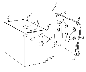
Conventional contact pads are used to make electrical interconnection with electrical
apparatus. In the present invention, the contact has a metal housing with a threaded bore
opening at one end into a circular well. A plated contact pad has a threaded stem screwed into
the bore and a circular pad member recessed in the well. The pad member has several cut-outs
around its edge, which are engageable by projections on a cooperating tool by which the
contact can be inserted and removed from the housing. Contact to the housing is made by
conductor secured to the housing by means of a bolt inserted in the rear end of the bore.


French Abstract

Des pastilles de contact classiques sont utilisées pour effectuer l'interconnexion électrique avec des appareils électriques. Dans la présente invention, le contact comporte un boîtier métallique présentant à une extrémité une ouverture filetée aboutissant dans un logement circulaire. Une pastille de contact plaquée comporte une tige filetée qui est vissée dans l'ouverture, ainsi qu'un élément circulaire encastré dans le logement. L'élément circulaire présente sur ses bords plusieurs encoches dans lesquelles peuvent s'engager les saillies d'un outil permettant d'insérer le contact dans le boîtier et de l'en retirer. Le contact avec le boîtier se fait au moyen d'un conducteur qui est fixé audit boîtier au moyen d'un boulon inséré à l'extrémité arrière de l'ouverture.

Claims

Note: Claims are shown in the official language in which they were submitted.


THE EMBODIMENT OF THE INVENTION IN WHICH AN EXCLUSIVE PROPERTY
OR PRIVILEGE IS CLAIMED ARE DEFINED AS FOLLOWS:
1. An electrical contact component comprising: a contact housing of a conductive metal,
said housing having an internally-threaded bore therein and a well, said bore opening
at one end into said well; and a contact pad of a conductive metal, said pad having an
externally-threaded stem screwed into said bore, and said pad having a planar pad
member received in said well.
2. A component according to Claim 1, wherein said pad member has a forward surface
recessed within said well.
3. A component according to Claim 1, wherein said bore opens at both ends of said
housing, and wherein the component includes an electrical conductor and a bolt
inserted in a rear end of said bore, said bolt securing said conductor to said housing.
4. A component according to Claim 1, wherein said pad member and said well are of
circular shape.
5. A component according to Claim 4, wherein said pad member has at least one
peripheral cut-out engageable by projections on a cooperating tool by which said pad
can be inserted and removed from said housing.

6. A component according to Claim 1, wherein said pad is of a metal and wherein said
pad member has a plated metal layer on at least a forward surface thereof.
7. A component according to Claim 1, wherein a part of an external surface of said
housing is non-circular to prevent rotation of said housing in a mounting hole.
8. A component according to Claim 1, wherein said housing has an externally-projecting
flange at a forward end.
9. Electrical apparatus including at least one electrical contact component, said contact
component comprising: a contact housing of a conductive metal, said housing having
an internally-threaded bore therein and a well, said bore opening at one end into said
well; and a contact pad of a conductive metal, said pad having an externally-threaded
stem screwed into said bore, and said pad having a planar pad member received in
said well.
10. Electrical apparatus according to Claim 9, including a plurality of said contact
components and a plurality of mounts by which cooperating equipment can be secured
with said apparatus.
11. An assembly of an electrical contact component and a tool, said contact component
comprising: a contact housing of a conductive metal, said housing having an
internally-threaded bore therein and a well, said bore opening at one end into said

well; and a contact pad of a conductive metal, said pad having an externally-threaded
stem screwed into said bore, and said pad having a planar pad member received in
said well, said pad member being of circular shape with at least one peripheral cut-out,
said tool having a projection engaging said cut-out by which said contact pad can
be unscrewed from said bore.
12. An electrical contact component comprising: a contact housing of a conductive metal,
said housing having an internally-threaded bore opening at opposite ends of said
housing, said housing having a circular well at one end of said housing, said bore
opening into said well; a contact pad of a conductive metal, said pad having an
externally-threaded stem screwed into said bore, and said pad having a circular planar
pad member received in said well with a forward surface of said pad member recessed
within said well; an electrical conductor; and a bolt inserted in a rear end of said bore,
said bolt securing said conductor to said housing.

Description

Note: Descriptions are shown in the official language in which they were submitted.


CA 022096~0 1997-07-03
ELECTRICAL COMPONENTS AND APPARATUS
Background of the Invention
This invention relates to electrical components and apparatus including such
components.
The invention is more particularly concerned with replaceable contact pad
components and a~pdldlLls including such components.
Where electrical connection is made to replaceable devices, this may be by means of a
butt contact, since connection is easily made and broken when the device is removed. The
contacting faces are prone to damage as a result of misuse and, for this reason, it is necessary
to replace the contacts regularly, which can be time consuming and expensive.
Brief Summar,v of the Invention
It is an object of the present invention to provide an improved electrical contact
component and a~paldlus including such a component.
According to one aspect of the present invention there is provided an electrical contact
component comprising a contact housing of a conductive metal, the housing having an
int~rn~lly-threaded bore therein opening at one end into a circular well, and a contact pad of a
conductive metal, the pad having an externally-threaded stem adapted to be screwed into the

CA 022096~0 1997-07-03
.
bore, the pad having a planar pad member adapted to be received in the well when the stem is
screwed in the bore.
The f~ v~d surface of the pad member is preferably recessed within the well. The
bore preferably opens at both ends of the housing, an electrical conductor being secured to the
housing by means of a bolt inserted in the rear end of the bore. The pad member and the well
are preferably of circular shape, the pad member having at least one peripheral cut-out
engageable by projections on a cooperating tool by which the pad can be inserted and
removed from the housing. The pad may be of metal and have a plated metal layer on at least
the forward surface of the pad member. A part of the external surface of the housing may be
non-circular to prevent rotation of the housing in a mounting hole. The housing may have an
externally-projecting flange at its forward end.
According to another aspect of the present invention there is provided appaldlus
including at least one contact component according to the above one aspect of the present
invention.
Apparatus including several contact components according to the present invention,
will now be described, by way of example, with reference to the accompanying drawing.
Brief Description of the Drawin.~
Figure 1 is a perspective view of the a~paialus;

CA 022096~0 1997-07-03
Figure 2 is a perspective view of one of the contact components to a larger
scale;
Figure 3 is a cross-sectional side elevation of the contact component; and
Figure 4 is a perspective view of one of the contact components illustrating
removal of the contact pad.
Detailed Description of the Preferred Embodiment
With reference to Figure 1, the appa dlus 1 takes the form of an electrical power
management system of which, only a part of the front panel 2 is shown. The front panel 2
supports two rows of three contacts 3 and four threaded apertures 4, which receive bolts 4'
projecting from electrical equipment 5 so that the equipment can be retained on the panel.
The equipment S has six contacts 6 positioned to mate with the contacts 3. The contacts 6 are
conventional cylindrical metal studs with a diameter of 12mm and with a flat end projecting a
short distance from the front face of the equipment. The contacts 6 are sprung loaded so that
they resiliently engage the contacts 3.
With reference now also to Figures 2 to 4, each contact 3 has a brass housing 30 of
circular section and tubular shape. The rear part 31 of the housing 30 is about 1 3mm in
diameter. About two-thirds the way along its length, the housing has an intermediate portion
32 of diameter about 1 5mm. The intermediate portion 32 is stepped out to form a short
forward portion 33 with a diameter of about 1 7mm, which is located in a mounting hole of

CA 022096~0 1997-07-03
the same size in the panel 2. One side of the fo~ ~d portion 33 is flattened to form a flat 34,
which locates with a similar formation in the mounting hole in the panel 2, to prevent rotation
of the contact 3 in the mounting hole. The housing could be given other non-circular shapes
to prevent rotation. The forward portion 33 also has a peripheral flange 35, of diameter about
24mm, overlapping the edge of the hole in the panel 2. At its forward end, the housing 30 has
a circular opening or well 36 with a diameter of 13mm and a depth of about 5mm. An axial
bore 37, of a diameter of about 4mm, extends through the housing 30, opening at both ends.
The rear end of the bore 37 receives a bolt 20 by which a tag 21 at the end of an electrical
power line or other conductor 22 can be electrically connected to the rear of the contact 3.
The contact 3 also includes a contact pad or button 38 machined from silver or some
other metal having a high electrical conductivity. The pad has a solid cylindrical stem 39
about 6mm long, which is externally threaded and has a diameter equal to that of the bore 37,
so that the stem can be screwed into the bore. The pad 38 is completed by a circular, radially-
projecting plate or pad member 40 about 12mm in diameter and about 1.3mm thick. The edge
of the pad member 40 is interrupted by four notches 41 equally spaced around its
circumference. The inner edge 42 of each notch 41 lies on a circle of diameter 10.5mm, the
sides 43 of each notch being formed by radii inclined at an angle 0 of 30~. The contact pad 38
has a protective, conductive coating provided by gold plating. When the contact pad 38 is
screwed fully into the housing 30, the forward surface of the pad member 40 is recessed
within the well 36.

CA 022096~0 1997-07-03
The contact pad 38 can be removed from, or inserted into, the housing 30 using an
insertion key 50, as shown in Figure 4. The insertion tool 50 is a cylindrical metal rod having
a square recess 51 at one end shaped to receive the head of a conventional driver (not shown),
such as of the kind used with socket spanners. The other end of the tool 50 has four
longitudinally-projecting teeth 52 of arcuate shape, the size and position of which are such
that the teeth can locate within the notches 41 in the contact pad 38, thereby enabling the tool
to be used to remove or insert the contact pad.
When the equipment 5 is mounted on the panel 2, the contacts 6 project into the well
36 of each contact 3 and resiliently contact the front surface of the pad members 40. If the
contacts 6 should become damaged as a result of misuse, or the like, the pads 38 are simply
unscrewed from the housings, using the tool 50, and replaced with alternative pads.

Representative Drawing
A single figure which represents the drawing illustrating the invention.
Administrative Status

2024-08-01:As part of the Next Generation Patents (NGP) transition, the Canadian Patents Database (CPD) now contains a more detailed Event History, which replicates the Event Log of our new back-office solution.

Please note that "Inactive:" events refers to events no longer in use in our new back-office solution.

For a clearer understanding of the status of the application/patent presented on this page, the site Disclaimer , as well as the definitions for Patent , Event History , Maintenance Fee  and Payment History  should be consulted.

Event History

Description Date
Inactive: IPC from MCD 2006-03-12
Application Not Reinstated by Deadline 2003-07-03
Time Limit for Reversal Expired 2003-07-03
Deemed Abandoned - Failure to Respond to Maintenance Fee Notice 2002-07-03
Inactive: Abandon-RFE+Late fee unpaid-Correspondence sent 2002-07-03
Letter Sent 2001-08-09
Application Published (Open to Public Inspection) 1998-01-04
Inactive: Filing certificate - No RFE (English) 1997-11-06
Classification Modified 1997-10-08
Inactive: First IPC assigned 1997-10-08
Inactive: IPC assigned 1997-10-08
Inactive: Filing certificate correction 1997-10-03
Inactive: Filing certificate - No RFE (English) 1997-09-15
Letter Sent 1997-09-15
Application Received - Regular National 1997-09-12

Abandonment History

Abandonment Date Reason Reinstatement Date
2002-07-03

Maintenance Fee

The last payment was received on 2001-06-07

Note : If the full payment has not been received on or before the date indicated, a further fee may be required which may be one of the following

  • the reinstatement fee;
  • the late payment fee; or
  • additional fee to reverse deemed expiry.

Patent fees are adjusted on the 1st of January every year. The amounts above are the current amounts if received by December 31 of the current year.
Please refer to the CIPO Patent Fees web page to see all current fee amounts.

Fee History

Fee Type Anniversary Year Due Date Paid Date
Registration of a document 1997-07-03
Application fee - standard 1997-07-03
MF (application, 2nd anniv.) - standard 02 1999-07-05 1999-05-19
MF (application, 3rd anniv.) - standard 03 2000-07-04 2000-06-22
MF (application, 4th anniv.) - standard 04 2001-07-03 2001-06-07
Owners on Record

Note: Records showing the ownership history in alphabetical order.

Current Owners on Record
SMITHS GROUP PLC
Past Owners on Record
NEIL ANDREW SWINDLEHURST
Past Owners that do not appear in the "Owners on Record" listing will appear in other documentation within the application.
Documents

To view selected files, please enter reCAPTCHA code :


To view images, click a link in the Document Description column. To download the documents, select one or more checkboxes in the first column and then click the "Download Selected in PDF format (Zip Archive)" or the "Download Selected as Single PDF" button.

List of published and non-published patent-specific documents on the CPD .

If you have any difficulty accessing content, you can call the Client Service Centre at 1-866-997-1936 or send them an e-mail at CIPO Client Service Centre.


Document
Description 
Date
(yyyy-mm-dd) 
Number of pages   Size of Image (KB) 
Representative drawing 1998-02-01 1 7
Abstract 1997-07-02 1 17
Description 1997-07-02 5 159
Drawings 1997-07-02 1 34
Claims 1997-07-02 3 87
Courtesy - Certificate of registration (related document(s)) 1997-09-14 1 118
Filing Certificate (English) 1997-09-14 1 165
Filing Certificate (English) 1997-11-05 1 164
Reminder of maintenance fee due 1999-03-03 1 111
Reminder - Request for Examination 2002-03-04 1 119
Courtesy - Abandonment Letter (Maintenance Fee) 2002-07-30 1 183
Courtesy - Abandonment Letter (Request for Examination) 2002-09-10 1 170
Correspondence 1997-10-02 2 74