Note: Descriptions are shown in the official language in which they were submitted.
CA 02209852 1997-07-08
WO 97/17193 PCT/US96/18096
EMBOSSED SUBSTRATE AND PHOTORECEPTOR DEVICE
INCORPORATING THE SAME AND METHOD
This invention relates to an embossed substrate and
photoreceptor device incorporating the same and method of
manufacture.
In photoreceptor belts utilized in copiers, various
thin layers have been utilized in the manufacture of such
belts. In order to increase the sensitivity of those belts,
it has been found to be desirable to make the thin layers
forming those belts still thinner and more planar. As these
layers have been made thinner or more planar, it has been
found that optical interference (moire effects) occurs within
the thin planarized overcoating. In other words, the moire
effects provide color or wood grain effects which are
particularly undesirable in laser printers because they
create constructive and/or destructive interference which
interferes with the images being printed. There is therefore
a need for a photoreceptor substrate which minimizes or
eliminates such optical interference and a method of
manufacture which makes possible the manufacture of such
a photoreceptor substrate.
In general, it is an object of the present invention
to provide an embossed substrate and photoreceptor device
incorporating the same and a method of manufacture which
minimizes or eliminates such optical interference effects.
CA 02209852 1997-07-08
WO 97/17193 PCT/LTS96/18096
-2-
Another object of the invention is to provide a
substrate, device and method of the above character in which
a surface is provided having a pattern which has a random
surface topography without periodicity that eliminates
optical interference effects.
Another object of the invention is to provide a '
substrate, device and method of the above character in which
the roughness of the embossed surface is controlled within
predetermined limits.
Another object of the invention is to provide a
substrate, device and method of the above character in which
the roughness has an average roughness ranging from 100 to
300 nanometers.
Another object of the invention is to provide a
substrate, device and method which can be used with laser
wavelengths ranging from 350 to 1050 nanometers.
Another object of the invention is to provide a
substrate, device and method of the above character in which
the pattern has peaks and valleys and in which the distance
between the adjacent peaks and/or valleys is greater than
the depth from the top of a peak and the bottom of an
adjacent valley.
Another object of the invention is to provide the
substrate, device and method which is suitable for use with
mass production techniques.
Another object of the invention is to provide a
substrate, device and method which can be utilized for
producing photoreceptor belts.
Additional objects and features of the invention will
appear from the following description in which the preferred
embodiments are set forth in conjunction with the
accompanying drawings.
Figure 1 is a cross-sectional view of a typical
substrate used in connection with the present invention.
CA 02209852 1997-07-08
WO 97/17193 PCT/US96/18096
-3-
Figure 2 is a cross-sectional view of etched glass the
surface of which is to be replicated in a method of the
present invention.
' Figure 3 is a cross-sectional view showing the etched
glass in Figure 2 being overcoated with a layer of
photoresist to provide a negative of the surface of the
etched glass shown in Figure 2.
Figure 4 is a cross-sectional view showing the
photoresist layer after it has been removed from the surface
of the etched glass.
Figure 5 is a cross-sectional view showing a positive
of the surface of the etched glass formed in a gold film
using the photoresist negative shown in Figure 4.
Figure 6 is a cross-sectional view showing the gold
film master which was created in the step shown in Figure
5.
Figure 7 is a cross-sectional view showing the manner
in which a metal shim is made utilizing the gold film master
to provide a shim having a negative image of the surface
of the etched glass shown in Figure 2.
Figure 8 is an isometric view showing an embossing
roller having a matted circumferential surface covered
with
a plurality of metal shims of the type made in the step
shown
in Figure 7.
Figure 9 is a schematic diagram showing apparatus
depicting the manner in which the pattern carried by the
metal shims on the embossing roller shown in Figure 8 are
transferred to provide an embossed film.
Figure 10 is a cross-sectional view showing the embossed
film produced in Figure 9 adhered to the substrate shown
in Figure 1 with the vacuum-deposited ground plane on top
of the embossed film.
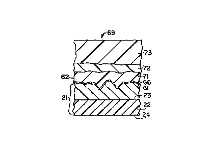
Figure 11 is a cross-sectional view of a photoreceptor
device incorporating the embossed substrate shown in
Figure l0.
CA 02209852 2000-OS-16
v 69767-15
4
In general, the embossed substrate of the present
invention is comprised of at least one layer of a plastic
material having an embossed surface. The embossed surface is
characterized in that it has a pattern with an average
roughness of between 100 nanometers and 300 nanometers with the
roughness being distributed substantially uniformly over the
surface. The pattern has ridges and valleys with the distance
between adjacent ridges or adjacent valleys being greater than
the depth between adjacent ridges and valleys. The ridges and
valleys are randomly disposed without periodicity in the
pattern to diffuse light impinging thereon to minimize or
eliminate interference effects when the embossed surface is
exposed to light.
According to another aspect of the present invention,
there is provided a photoreceptor device comprising at least
one layer of a plastic material having an embossed surface,
said embossed surface having a pattern with an average
roughness of between 100 nanometers and 300 nanometers with the
roughness being distributed substantially uniformly over the
embossed surface, said pattern having ridges and valleys with
the distance between adjacent ridges or adjacent valleys or
adjacent ridges and adjacent valleys being greater than the
depth between the tops of the ridges and the bottoms of the
valleys, the ridges and the valleys being randomly disposed
within the pattern without periodicity, a ground plane layer
adherent to the embossed surface, a charge blocking layer
adherent to the ground plane layer, a charge generation layer
adhered to the charge blocking layer and a charge transport
layer adherent to the charge generation layer, said embossed
surface serving to cause diffusion of light impinging thereon
and serving to minimize or eliminate optical interference
effects when the photoreceptor device is exposed to light.
CA 02209852 2000-OS-16
69767-15
4a
According to a further aspect of the present
invention there is provided a method for providing a shim
having an embossed surface, the method comprising: (a)
providing a replica of a surface with an average roughness of
between 100 nanometers and 300 nanometers, the roughness being
distributed substantially uniformly over the surface and with a
pattern having ridges and valleys with the horizontal distance
between adjacent ridges or adjacent valleys or adjacent ridges
and adjacent valleys being greater than the vertical distance
between the tops of the ridges and the bottoms of the valleys,
the ridges and valleys being randomly disposed in the pattern
without periodicity; and (b) creating an embossed surface on a
surface of the shim corresponding to the replicated surface.
More in particular as shown in Figures 1 through 11
of the drawings, an embossed substrate 21 incorporating the
present invention is shown in Figure 10 and is made utilizing a
substrate 22 shown in Figure 1 in conjunction with the steps
shown in Figures 2 through 9. The substrate 19 has upper and
lower surfaces 23 and 24. The substrate 22 can be formed of
any suitable material put preferably is formed of a flexible
material as for example a plastic such as PET having a
thickness ranging from 1 to 10 mils and preferably a thickness
of 2-3 mils and in which the surfaces 23 and 24 do not have the
desired roughness necessary for implementation of the present
invention. Thus, for example, the surface 23 can have an
average roughness Ra of 78 nanometers or less which is too
smooth and conversely if the surface 23 has an average
roughness Ra of 400 nanometers it is too rough. In accordance
with the present invention it is desirable to provide a surface
having an average roughness Ra ranging from 100 to 300
nanometers and preferably from 120 to 250 nanometers.
As hereinafter described, one of the surfaces 23 and
24 can be directly embossed to provide the desired roughness.
CA 02209852 2000-OS-16
69767-15
4b
When this approach is utilized, it is desirable that the
substrate 22 be provided with a hard coat on the surface 23
formed of a suitable material such as an acrylic. Such
CA 02209852 1997-07-08
WO 97/17193 PCT/US96/18096
-5-
a starting substrate is available commercially and can be
identified as TEKRA Marnot II supplied by TEKRA, a PET
substrate with an embossable acrylic hardcoat.
In the method hereinafter described for producing the
embossed substrate 21, a substrate 22 without such a hard
r coat is utilized. In accordance with the present invention
in order to find a pattern which can be embossed onto the
substrate 22, various surfaces were investigated for copying
or replicating to provide such an embossed surface. One
article,found which exhibited a desired pattern was found
in a piece of glass 26 which had an etched surface 27
identified as a 90 gloss etched glass. In connection with
the present invention it is believed that a gloss ranging
from 60 to 97 gloss can be utilized although a 90 gloss
is preferable. The surface topography 27 of such a glass
can be characterized in a number of ways as set forth below
wherein the replication of the surface of the glass is
discussed. Typically the 90 gloss etched glass has a
pattern with an average surface roughness ~ of approximately
150 manometers with a range of between 110 and 150 manometers
occurring in such an etched glass surface. RMS averages
of 140 and 200 manometers and Z averages of 430 and 410
manometers for the depth were measured. A scan profile of
the scan profile sample etched surface of the etched glass
shown in Figure 2 extended over 400 micrometers. The
distance between adjacent valleys and/or peaks was
approximately 10 micrometers with the depth from the top
of a peak to the bottom of a valley being approximately
400
manometers . thus it can be seen that the width between
adjacent valleys and/or peaks should be greater than and
preferably substantially greater as for example a factor
of 20 or more than the depth between a peak and an adjacent
s
valley. The pattern provided by the surface of such 90
gloss etched glass was random without periodicity on a
microscale.
CA 02209852 1997-07-08
WO 97/17193 PCT/US96/18096
-6-
Although glass has been utilized for providing the
desired surface characteristics for embossing as hereinafter
described, other materials also can provide the desired
surface characteristics as, for example, plastic and metal
sheets.
It should be appreciated that rather than copying or
replicating a pattern which is provided by a surface of a
physical article, a similar pattern can be produced by the
use of a computer to provide a similar surface topography
such as the form of a three-dimensional damped sinusoidal
wave where the high amplitude peaks are randomly spaced
across the surface. By way of example, the width or spacing
between adjacent peaks could be approximately 10 microns
whereas the depth from the top of a peak to the bottom of
a valley could be approximately 0.1 micron. The damping
is required to prevent the formation of a diffraction
grating. In other words the pattern formed should be diffuse
and random to avoid periodicity on the surface and also to
avoid diffraction effects.
Assuming that the desired surface has been chosen which
it is desired to replicate in accordance with the present
invention, the glass substrate 26 shown in Figure 3 has the
surface 27 coated with a release film 31 formed of a suitable
material such as silicone oil to a thickness of approximately
0.1 micron or less. A photoresist layer 32 is deposited
over the release film 31 in a suitable manner such as by
supplying a liquid negative photoresist in the form of a
photopolymer as for example, an Eastman Kodak photoresist
and spinning it onto the surface of the release film 31 and
drying the same in a conventional manner.
After the photoresist layer 32 has dried or cured, the
photoresist layer 32 is stripped from the surface 27 of the
etched glass substrate 26 to provide a negative replica of
the surface 27 of the etched glass 26 as shown in Figure 4.
CA 02209852 1997-07-08
WO 97/17193 PCT/US96/18096
_7_
In the event that the desired embossed surfaces is created
by a computer, the photoresist master 32 may be created
using
e-beam lithography techniques utilizing the computer
generated pattern. The photoresist layer 32 has a surface
33 which is a negative of the surface 27 which is desired
to replicate. This surface is utilized to provide a positive
replica master shim 36 having a surface 37 which creates
a positive replication of the etched surface 27 of the glass
substrate 26. Conversely, if desired, a negative replica
master shim can be provided which creates a negative
replication of an etched surface. This shim 36 can be formed
of a suitable material such as gold in a conventional
electroless plating method to provide a gold master shim
36 having a surface 37 which is a positive replication of
the surface 27 of the glass substrate 26. As soon as the
gold film master 36 has been formed, the photoresist layer
32 can be dissolved or washed away in a conventional manner
so that there remains a gold film master shim 36 having
the
surface 37 as shown in Figure 6. By way of example, the
shim 36 can be of a suitable size as for example 1/2" by
1/2" square.
A plurality of tiling shims 41 are then formed from
the gold film master shim 36 to provide surfaces 42 on the
shims 41 which are the negatives of the surface 27 of the
glass substrate 26 and a surface 43. To accomplish this,
a release layer 44 formed of a suitable material such as
a silicone oil or sodium chloride is placed on the surface
37 of the master shim 36 and thereafter a metal such as
nickel is electroplated in an electroless plating technique
onto the surface 37 to a suitable thickness as for example
10 microns. After the plating has been finished, the release
layer 44 is dissolved so there remains the surface 42 which
' carries the second negative image of the etched surface
27
of the glass 26. The nickel shims can have suitable
.. 35 dimensions as for example the same 1/2" by 1/2" dimensions
as the gold film master shim 36.
CA 02209852 1997-07-08
WO 97/17193 PCT/US96/18096
_g_
It should be appreciated that in connection with the
present invention it has been found that it is possible to
utilize a negative replication of the surface. In order
to create a negative replication of the surface, it is only
necessary to make one more generation of the embossing shims,
shifting the tiling shims from negative to positive.
In accordance with the present invention let it be
assumed that it is desired to tile an embossing roller 46
having a cylindrical surface 47. The roller 46 can be formed
of a suitable material such as stainless steel or aluminum.
For example, utilizing a cylindrical surface having a
diameter of 6'° inches and a width of 36" and utilizing tiling
shims 1/2" square, in excess of 2000 shims would be required
to cover that surface. The nickel tiling shims would then
be taken and have their surfaces 43 secured to the
cylindrical surface 47 by adhering the surfaces 43 to the
cylindrical surface 47 by a suitable means such as an
adhesive (not shown) and placing the shims 46 side by side
and end to end in a matte to provide a surface pattern
corresponding to the surfaces 42 of the shims 41 facing
outwardly and radially from the cylindrical surface 47 to
provide a cylindrical embossing surface. After the shims
41 have been tiled in a matte format onto the surface 47,
the roller 46 can be used to directly emboss the pattern
carried thereby onto the hard coated surface of a flexible
substrate as for example the PET substrate carrying an
acrylic hard coat. This can be accomplished by use of a
suitable temperature and pressure as for example a
temperature of 150°C and 80 pounds per square inch and
running the substrate between the embossing cylinder and
a smooth steel roller.
Alternatively, the embossing roller or cylinder 46 can
be utilized in an apparatus and system such as shown in
Figure 9. The PET substrate 22 is carried on a supply reel
51 and travels between the embossing roller 46 and a glass
roller 52 that has an ultraviolet light source 53 therein
and is then taken up by a take up reel 54. As also shown
CA 02209852 1997-07-08
WO 97/17193 PCT/US96/18096
-9-
in Figure 9, the embossing roller 46 travels through a
liquid
in the form of an ultraviolet (W) curable polymer bath
56
disposed within an open top tank 57. The curable polymer
' bath can be in the form of a W curable acrylic polymer
or
an epoxy based polymer within a fast cure heat curable
polymer system using an IR heat source. During operation
of the apparatus shown in Figure 9, the embossing roller
46 picks up a thin layer of the ultraviolet curable polymer
from the bath 56 and engages the other under side or lower
surface 24 of the substrate 22 and squeezes the polymer
from
the bath into the pattern on the shims 41 carried by the
embossing roller 46. A doctor blade 64 can be utilized
to
remove excess polymer from the embossing roller before
the
polymer arrives at the underside of the flexible substrate
22. The polymer in contact with the embossing roller 46
is cured by the W light source 53 to provide a cast embossed
film 61 adherent to the surface 24 of the substrate 22
and
to cause the layer 61 to be formed of a suitable thickness
as for example 2 microns and to separate from the embossing
roller 46 as it continues to rotate. The cured polymer
layer
61 then travels with the substrate 22 as an embossed
substrate 21 onto the take-up reel 54. After completion
of the operation shown in Figure 9, the take up reel 54
can
be shipped to the customer where it can be utilized for
making photoreceptor devices of the type hereinbefore
described. The layer 61 provides an embossed surface 62
for the substrate 22 which is a positive or negative of
the
pattern provided by the etched surface 27 of the glass
substrate 26 which it was desired to replicate.
Alternatively before shipping the reel 54 to the
customer, the surface 62 can be provided with a vacuum
deposited ground plane 66 formed of a suitable material
such
as metal. This can be readily accomplished by passing the
embossed substrate 21 carried by the take up reel 54 and
advancing the same through a conventional vacuum chamber
to metalize the surface 62 to provide a conformal coating
serving as the ground plane by evaporating aluminum or
other
CA 02209852 1997-07-08
WO 97/17193 PCT/US96/18096
-10-
suitable metallic material inside the vacuum chamber. After
the metalized ground plane 66 has been provided on this
surfaoe 62, the embossed and metalized substrate can then
be wound up on another take-up reel (not shown) and
thereafter shipped to the customer for fabrication into
photoreceptor devices.
The embossed substrate 21 with or without the vacuum
deposited ground plane 66 can be utilized for making
photoreceptor devices as for example the device 69 shown
in Figure 11. As shown therein, the embossed surface 62
was provided with the ground plane 66 as hereinbefore
described followed by a series of organic coatings of a type
well known to those skilled in the art. Thus there can be
provided a subbing adhesion layer/charge blocking layer 71
overlying the ground plane 66. This is followed by a charge
generation layer 72 and a charge transport layer 73 to
provide the finished product 69. By way of example, the
PET substrate 22 can have a suitable thickness as for example
75 microns. The cast embossed film or layer can have a
suitable thickness as for example 2 microns. The ground
plane can have a thickness of less than 0.1 microns.
Typically the subbing adhesion layer or /charge blocking
layer 71 can have a thickness greater than 1 micron and the
charge generation layer 72 can have a thickness ranging from
0.1 to 1 micron and the charge transport layer 73 can have
a thickness of 20 microns.
With the construction shown in Figure 11 the
photoreceptor device 69 is provided with an embossed surface
62 which overlies the substrate 22 and provides a light
diffusing capability for the photoreceptor device 69 which
minimizes or eliminates optical interference (moire) effects
such as color or wood graining in the image emitted through
the charge transport layer 73 even though thin planar organic
layers may be utilized which overlie the ground plane 66.
The embossed surface 62 as described in connection with the
surface 27 of the glass 26 has a topography in which the
ridges and valleys provided are in a randomized non-periodic
CA 02209852 1997-07-08
WO 97/17193 PCT/US96/18096
-11-
pattern and in which the ridges and valleys are more widely
spaced from each other than the vertical distance between
the peaks and the valleys to provide a microscale topography
which diffuses light and does not have any coherent
interference effects. The average roughness Ra should be
less than 300 manometers and greater than 100 manometers.
With such a topography, the photoreceptor device can be
utilized with laser printers typically using infrared laser
diodes for a light source having a wave length ranging from
l0 780 to 950 manometers. Thus the present invention is
particularly applicable to IR laser copiers and printers.
However, the same type of photoreceptor device as described
in the present invention can be utilized in white light
copying machines.
Although the present invention has been described
principally in connection with a flexible plastic films,
it should be appreciated that the same principles can be
utilized in connection with flat surfaces such as those
provided on flat plastic plates. From the foregoing it
can be seen that there has been provided an embossed
substrate which can be utilized in photoreceptor devices
to minimize or eliminate optical interference effects when
the layers making up the photoreceptor device are made
thinner and more planar.