Note: Descriptions are shown in the official language in which they were submitted.
CA 02210048 1997-07-23
WO 96!24142 PGT/US96101573
1
MOLDED CABLING, PREFORM FOR MAKING
AND METHOD OF MAKING
Field of the Invention
The present invention is directed to a molded
cabling, a method of making and a preform for use in the
molded cable making method.
Backctround Art
Electric cables come in a wide variety of shapes,.
types of conductors, number of conductors, insulation,
and configurations. Electrical cables can be as simple
as a single conductor with a simple insulator on the
exterior of the conductor, or they can be very complex
having multiple conductors of different sizes and
different types with varying terminations or exit points
along the length. The cabling can also have various
termination devices on the ends of the conductors or they
can be left bare, depending on the particular
application.
Electrical cables of some sort are used in
practically every device incorporating any electronics or
electronic devices. Cabling is required to tie in the
source of electricity to the electronics and to deliver
and transfer electronic signals to other electronic.
device, to gauges, meters, lights or other visual
indicators, to allow communications between devices and
coordination of activities. Any time any type of
electronic signals or current has to be delivered or
transferred from one device to another electrical cables
are generally in use.
Typically, when there are multiple signals or
currents being transmitted between devices in most modern
day apparatuses or machines, a custom electrical cable
CA 02210048 1997-07-23
WO 96124142 PGT/US96101573
2
having multiple conductors and multiple terminations are
made. Custom made electrical cables are used in
automobiles, trucks, airplane, jets, rockets, other types
of military apparatuses, computers, televisions, some
telephones, .stereos, and practically every other device
imaginable employing any type of electronics. '
In the past electrical cables have been made by
several different configurations and methods. Typically,
multiple conductors are contained within a sheath or
covering . The sheath can be wrapped or molded by several
different types of methods known in the art. Molding
techniques result in a cable having multiple conductors
surrounded by some sort of molding compound. The cable
can be in one of several different configurations. The
cable can be a flat ribbon, or round in the most common
configurations. The multiple conductors can all run
parallel to each other or they can be wrapped around each
other in some sort of woven pattern, depending on the.
particular application and types of conductors.
In one instance of the prior art, electrical
conductors are woven in a particular pattern such that
the primary signal wire has non-signal carrying wires
wrapped around it. This provides protection from
interference from other signals. The non-signal wires
can be current carrying conductors or ground conductors.
The woven wires are then surrounded by an insulating
material in most instances.
Particular applications having custom cabling often
have conductors entering and leaving the cable at several
different locations, with each having some sort of
termination device. These type of cables are often
prepared in some sort of jig designed specifically for
the particular application. The wire are installed
individually or in particular groups along the jig. Each
of the wires or groups are added to the cable at '
particular locations leaving a sufficient length
CA 02210048 1997-07-23
WO 96/24142 PGT/US96/01573
3
extending from the cable for a termination device and to
enable the termination device to connect to some
electrical apparatus. Once all the wires are in place,
the cable is wrapped with an insulating material or
subj ected to a molding process where the cable is covered
in the insulating material. The insulating material in
the later often completely fills all voids between the
wire and completely surrounds the wires forming an
exterior insulating material around the cable..
The cabling of the prior art has several
disadvantages. Once multiple conductors are included
within a cable it is very difficult to make a repair to
a single conductor. Typically, the cable outer
insulating material has to be removed over a significant
length to locate the problem and most be completely
removed from end to end if the conductor has to be
replaced. If the conductors are included in any sort of
woven pattern, a single conductor typically can not be
removed or repaired. If the conductor is included in any
sort of molded sheath it may be impossible to remove or
repair a single conductor without destroying the
integrity of the cable.
Another disadvantage is the weight of the insulating
material used in making the cable. Weight of the
insulating material in some instances may actually exceed
the weight of the conductors in the cable. Some
applications where electrical cabling is used may be very
critical. This is especially true in instances where the
apparatus in which the cable is used has some sort of
motion or locomotion, such as in automobiles, aircraft,
spacecraft, and other military and non-military
applications just to name a few.
United States Patent No. 5,331,115 to Ysbrand
discloses a molded cabling and a method of production
which overcomes the disadvantages noted above. In this
patent, a molded woven cabling is produced using
_ CA 02210048 1999-07-12
4
injection molding techniques. Treat is, a plurality of
wires or conductors are placed in a mold followed by an
injection molding step which forms a harness around the
conductors and the molded cable. One of the drawbacks
associated with this process is that the conductors or
wires used during the injection rr~olding can be adversely
affected by the injection molding step.
As such, a need has developed to provide an improved
molding technique for making these types of molded
cablings. In response to this need, the present
invention, in one aspect thereof, provides a new and
improved molding method using a preform which can be
subsequently removed for insertion of the desired
conductors. In another aspect, the present invention
provides an improved harness structure for molded
cabling.
Summary of th Tnvant;nn
Accordingly, it is an object of the present
invention to provide a molded cabling overcoming several
disadvantages of the prior art.
Another object of the present invention is to
provide a molded cable that is constructed to provide a
cable in which the overall weight of the cable is
significantly reduced compared to similar cables
currently known in the art.
A further object of the present invention is to
provide a molded cable in which a .single conductor within
the cable can be readily removed, repaired, or replaced
without compromising the integrity of the entire cable.
CA 02210048 1999-07-12
Yet another object of the present invention is to
provide a molded cable having a greater degree of
flexibility.
It is a further object of the present invention to
provide a molded cable which utilizes a diamond-shaped
webbing as the cable harness.
Other objects and advantages of the present
invention will become apparent a;s a description thereof
proceeds.
In satisfaction of the foregoing objects and
advantages, the present invention comprises a molded
cable having a plurality of conductors forming the cable,
the conductors being positioned in spaced relationship
with each other. The conductor; are surrounded by a
plastic-like molding compound molded into a web.
Alternatively, the web can bE~ made with a series of
channels therethrough for receiving the conductors after
the web has been manufactured.
The web preferably comprises opposing end portions
and side portions with a web portion extending
therebetween. The web portion further comprises a
plurality of strands, the strands extending between the
opposing end portions and intersecting each other to form
diamond shaped openings. At each intersection of a pair
of strands is a channel permitting passage of at least
one conductor therethrough.
To accomplish the foregoing and other objects of
this invention there is provided molded cabling for
electrical conductors in which a plastic like material is
molded in place around the individual conductors.
The above mentioned objects and other objects and
features of the present invention will be better
CA 02210048 1999-07-12
6
understood and appreciated from the following detailed
description of the main embodimer..t thereof, selected for
purposes of illustration and shown in the accompanying
drawings.
CA 02210048 1997-07-23
WO 96/24142 PCTIUS96101573
7
Brief Description of the Drawings
Reference is now made to the drawings of the
invention wherein:
Figure 1 is a top view of a molded cable showing a
plurality of conductors with conductors exiting the
cable at different location.
Figure 2 is a bottom view of the beginning of the
molded cable.
Figure 3 is a sectional view of the molded cable.
Figure 4 is a representation of a mold holding a
molded cable.
Figure 5 is an illustration of a mold used to
produce a molded cable of this invention.
Figure 6 is a perspective view of another
embodiment of the invention showing a molded cable
utilizing a web pattern.
Figures 7-9 are cross-sectional views along the
lines VII-VII, VIII-VIII and IX-IX of Figure 6.
Figure 10 is a top view of an exemplary preform of
the invention.
Figure 11 is a top view of another embodiment of.
the molded cable using a web pattern.
Figure 12 is a perspective view of a portion of
molded cable of Figure 6 enlarged for greater
detail.
CA 02210048 1997-07-23
WO 96!24142 PCT/US96101573
8
Description of the Preferred Embodiments
Ref erring now to the drawings , f figures 1 through 3 ,
there is shown one preferred embodiment showing the
principle characteristics for the molded cabling of the
present invention. The molded cable 10 of this invention
generally consists of a plurality of conductors 12 held
in a space relationship by a woven plastic like compound
28.
The preferred embodiment and the best mode
contemplated of the molded cabling and a method of
production of the present invention are herein described.
However, it should be understood that the best mode for
carrying out the invention hereinafter described is
offered by way of illustration and not by the way of
limitation. It is intended that the scope of the
invention include all modifications which incorporate its
principal design features.
There can be as few as three conductors to an almost
unlimited number of conductors included in the molded
woven cabling 10 of this invention. Generally, the morE
conductors included the more complex the woven pattern
becomes, especially if more than one layer is required.
The conductors 12 can be generally referred to as a first
.conductor 14 , second conductor 16 , and continuing in this
manner to a last conductor 18. The conductors 12 are
held in a spaced relationship with each other by the
plastic like compound 24 interlaced with the conductors
12 in a woven pattern 30. Preferably, the plastic like
compound 24 is a molding compound which can be used in
the molten state or can be a two part compound such as
polyurethane with a curing agent.
For descriptive purposes, the woven pattern 30 of
the plastic like compound can be described as a narrow
strip 28 of the plastic like compound 24. However. in
the preferred embodiment the narrow strips 28 are
actually formed by a molding compound injected into a
CA 02210048 1997-07-23
WO 96/24142 PGTIUS96I01573
9
mold forming the woven pattern 30 along the entire length
almost simultaneously. First, the plastic like compound
24 forms a beginning base 26 around the conductors 12
near the beginning end 20 of the molded woven cable 10.
This secures,all the ends 20 of the conductors 12 in a
spaced relationship. The narrow strip 28 is then woven
over the first conductor 14, under the second conductor
16, over the third conductor and continuing in this
weaving pattern until the last conductor 18 is included.
The narrow strip 28 is then woven around the last
conductor 18 and woven back over the conductors 12 in the
opposite manner to the first conductor 14 weaving the
conductors together and securing them in a spaced
relationship. The weaving pattern is repeated to an
ending position 32. The narrow strip 28 then forms an
ending base 34 around all the conductors 12 that
terminate near the ending position 32.
The beginning base 26 and the ending base 34 secure
all the conductors together to maintain the spaced
relationship to each other at the beginning and end of
the molded cable 10. Without the bases 26 and 34, the
conductors 12 would be free to laterally move down to the
first woven strip of the plastic like compound. This
could result in weakening the structure of the molded
cable at these locations.
There are virtually unlimited configurations which
can be made using the molded cable 10 of this invention
and then method of production. As illustrated in ffigures
1 and 4, there is a single beginning 20 and three
separate ending locations 22. The exact configuration of
the cable, the number and location of beginnings and
endings, and the type of terminations would be determined
by the particular application. The description and
illustrations are not meant to limit the scope and
application of this invention. There could be multiple
entries and multiple exits in any given application. In
CA 02210048 1997-07-23
WO 96/24142 PCTIOS96/01573
addition, there could be multiple cables all configured
differently in one apparatus.
Significant advantages are achieved by the molded
cabling 10 of this invention. This includes; a greater
5 flexibilityd weight reduction, and repairability of
conductors within the cable, just to name the most '
obvious. Since the conductors are not secured and
totally secured within a sheath, either wrapped or
molded, the conductors have more freedom to move. The
10 conductors 12 can slide between the narrow strip 28
within the woven pattern 3 0 . This allows the cable a
greater amount of flexibility than other type of cabling
known in the art.
Since the plastic like material only covers
approximately half of the outer surfaces of the
conductors 12 and the void areas between the conductors
are not filled, only about half or less material is
needed. Since only half the material is used the weight
is significantly reduced.
Repairability of the conductors 12 within the molded
cabling 10 is possible. This is due to the fact that the
conductors 12 within the cabling 10 have the freedom to
slide within the woven pattern 30 and about half of the
outer surface of the conductors 12 can be observed.
Therefore, the problem area can be readily observed and
accessed. A single conductor, or more, can be pulled out
of the woven pattern 30 and replaced back into the weave
without destroying the integrity of the cable. This is
not typically possible in the cabling currently known in
the art . Typically, in the current art the sheathing has
to be removed or split in order to observe and access a
conductor contained within. Therefore, in most instances
the entire cable is replaced rather then repaired.
As indicated above the, the plastic like compound 24
is a molding compound in the preferred embodiment. As
shown in f figure 4 , the woven pattern 3 0 , in the preferred
CA 02210048 1997-07-23
WO 96/24142 PCTIUS96I01573
11
embodiment, is formed by~an injection molding process
although other suitable molding processes may be used.
A primary injection port is represented by reference
numeral 36. The molding compound is injected into the
primary injection port 36 and flows down through ari
injection channel 38 to individual injection ports 40.
In the preferred embodiment as shown, each individual
injection port 40 forms two narrow strips 28 of the
plastic like compound. In design all the individual
injection ports 40, should be injecting the molding
compound into the woven pattern 30 at the same time.
Therefore, all the narrow strips 28 should be formed at
about the same time.
The excess molding compound exits through exit ports
42 on the opposite side of the molded cable 10 from the
individual injection ports 40. The molded cabling 10
should not be complete unless there is an excess coming
out of all exit ports 42. This insures that all of the
narrow strips 28 are completely formed before the mold 50
is removed.
The first step in the production of the molded
cabling 10 of this invention is to create the mold 50,
illustrated in figure 5. The mold 50 can be produced by
any of several methods known in the art. The mold 50
will have slots 52, a woven pattern 30, injection ports
40 and exit ports 42. The slots 52 correspond to the
size, number and desired configuration of the conductors
12 and the final cable 10 to be produced. The mold 50
will also have a primary injection port 36 for the
receipt of the molding compound. In the preferred
embodiment, there will be a primary injection port 36
leading to an injection channel 38. Individual
injections ports 40 from the injection channel 38 will
feed the woven pattern 30 at various points along the
length. Typically, the points will corresponding to-
every other weave of the woven pattern. There will also
CA 02210048 1997-07-23
WO 96/24142 PGTJtTS96101573
12
be cutout area 44 for the beginning base 26 and cutout
area 46 for the ending base 34.
Once the molds are complete, the next step would be
to install the conductors 12 into the slots 52 and '
complete the,assembly of the molds 52 with conductors 12
getting the assembly ready for the injection of the '
molding compound.
The molding compound would then be inj ected into the
primary injection port 36 using any one of the injection
processes known in the art. The molding compound would'
flow through the injection channel 38 into the individual
injection ports 40 and into the woven pattern 30. Once
the woven pattern 30 is completely filled, the excess
molding compound would exit the exit ports 42.
Then depending on the particular molding compound,
a curing cycle may be initiated to allow the molding
compound to properly set and harden. Once properly cured
the mold 50 can be removed leaving a molded cable 10.
The excess and any flashing would have to be cleaned to
provide the completed and finished product.
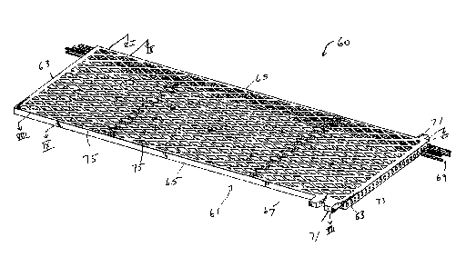
With reference to Figure 6, another embodiment of
the inventive molded cabling is generally designated by
the reference numeral 60 and includes a cable harness
which may house one or more conductors as will be
described hereinbelow.
The cable harness 61 has opposing end portions 63
and opposing side portions 65. Arranged within the
periphery formed by the end and side portions is a web
portion 67. The harness 61 may also have tabs 71 which
facilitate mounting the harness for a given application.
Other tab configurations may be used depending on the
desired end use, the tabs being positionable anywhere on
the harness.
With reference to Figures 6-9, the end portions 63
of the harness include spaced apart channels 73 which are -
CA 02210048 1997-07-23
WO 96/24142 PGTlUS96101573
13
sized to receive one or more wire conductors in each
channel.
Referring now to Figures 6 and 12, the web portion
67 is made of a series of strands 75 which extend within
the periphery of the harness 61. Each strand 75 extends
between an end portion and a side portion. The strands
75 are angled with respect to each other and the end and
side portions 63 and 65 to form diamond shaped openings
77. In conjunction with formation of the diamond-shaped
openings 77, the strands 75 form intersecting portions as
designated by the reference numeral 79. At each of these
intersecting portions is a channel 81 which is formed
during the molding process and is sized to receive wire
conductors for the finished molded cable.
By reason of the angulation of the strands 75 to-
form the diamond-shaped openings 77, each strand
comprises a short segment 83 between adjacent
intersecting portions 79 or one of the end or side
portions of the harness 61. The cross-sectional views of
the inventive harness in Figures 7-9 show the
relationship between the segments 83, channels 81, and
the intersecting portions 79. Within the scope of the
present invention the openings 77 may have other shapes
then diamond shapes, e.g. oval, square, or the like.
The channels 81 in the intersecting portions 79 and
the channels 73 in the end portion 63 align to provide
longitudinal passageways 85 through the harness 61 for
one or more wire conductors. As described above, the
cable harness 61 may be manufactured with the wire
conductors already in the passages 85 or, alternatively,.
as will be described in greater detail hereinbelow,
manufactured with a preform followed by preform removal
and wire conductor insertion.
Figure 11 depicts an alternative configuration of
the molded cable designated as reference numeral 60'.
This configuration shows that different shapes or types
CA 02210048 1997-07-23
WO 96124142 PCTIUS96I01573
14
of end portions 63' or tabs 71' can be used with the
inventive molded cable depending on the desired end use.
The molded cable 60' shown in Figure 11 is also exemplary
of the configuration of the mold surface used during
molded cable manufacture. That is, the mold surface
follows a generally circular path to form the molded '
cabling 60'.
When manufacturing the molded cabling 60 with
conductors in place, the molding process for making the
woven cabling described above can be followed. That is,
the molded cabling 60 is formed with the conductors in
place.
Alternatively, the cable harness 61 can be
manufactured using a preform as shown in Figure 10. In
this method, the cable harness 61 is first formed by
molding with the preform. The preform can then be
removed and replaced with the desired number of
conductors to form the molded cabling.
With reference to Figure 10, an exemplary preform is
generally designated by the reference numeral 100 and
includes a plurality of preform strands 101. The preform
strands are longitudinally aligned and j oined by a strand
connector 103. The strand connector 103 is preferably
injection molded directly to the preform strands 101 when
the preform is manufactured. The preform 100 is
preferably molded out of a molding compound such as a
plastic, e.g. polyurethane of various hardnesses, or a
silicone of various hardnesses. Alternatively, the
preform 100 can be a metallic material such as stainless
steel with the strand connector being metallic or non-
metallic and attached using conventional means. Likewise
the strand connector could be metallic and the strands
being non-metallic.
The strand connector 103 can include recesses 105
therein which facilitate positioning of the preform when
used to form the cable harness 61.
CA 02210048 1997-07-23
WO 96/24142 PCTIUS96101573
It should be understood that the strand connector
103 can take any shape or configuration and be located at
any point along the strand lengths. As shown in Figure
10, the strands can increase successively in length so
5 that when the preform 100 is used in a mold as depicted
in Figure 11, the preform strand ends 107 will terminate
roughly in alignment with an end portion of the molded
cabling 60'.
The preform 100 is preferably injection molded and
10 can be molded such that the strands are all aligned
longitudinally or, alternatively, formed in a circle
similar to the configuration shown in Figure 11.
In a method of forming the cable harness 61, a
preform 100 is first positioned in the mold. Preferably,
15 the mold comprises two mold halves with the preform
arranged on one mold half initially. The other mold half
is placed thereon, the two halves clamped together and
injection molded with a molding compound such as
polyurethane. Following filling the mold, the mold is
placed in an elevated temperature oven to cure.
After curing is affected and the mold is cooled to
ambient temperatures, the mold is opened and the cable
harness and the preform combination is removed. The
preform is then removed from the cable harness, this
removal step leaving hollow tunnels or channels in the
web portion 67 of the harness 61, see Fig. 12.
The desired electrical conductors are then inserted
into the hollow channels to create the molded cabling
comprising both the cable harness and electrical
conductors. With the conductors in the harness, the
wires are held in the position of zero stress and have
not been exposed to any high temperatures since the
preform has been used during the mold curing step. Thus,
the wires have an extended life. Further, as described
above, each and every wire is completely replaceable by
CA 02210048 1997-07-23
WO 96/24142 PCTIUS96101573
16
removal from the cable harness followed by replacement of
another wire or wires.
During the molding process, if necessary, a parting
compound could be utilized to assure separation of the
preform from the cable harness once the product is
removed from the mold. It should also be understood that '
the web pattern formed in the molding process can have
different cross-sectional shapes for the strands thereof.
For example, the strands could be oval, circular or
square in shape or rectangular as shown in Figure 12.
The dimensions of the web pattern can also be altered
depending on the desired end use and the type .of
conductors being utilized in the molded cabling. For
example, large diameter conductors would require web
dimensions sufficient to form the channels for receiving
the conductors. Likewise, the small diameter conductors.
can be accommodated with smaller dimensioned webs. In
addition, any number of conductors can be utilized with
the inventive molding cable and method of making. The
preform can also accommodate any number of strands to
coincide. with a desired number of conductors for a given
application.
The embodiment depicted in Fictures 6-12 can
incorporate any of the features described above for
Figures 1-5.
As such, an invention has been disclosed in terms of
preferred embodiments thereof which fulfill each and
every one of the objects of the present invention as set
forth hereinabove and provides a new and improved molded
cable, method of making and preform for use with the
inventive method.
Of course, various changes, modifications and
alterations from the teachings of the present invention
may be contemplated by those skilled in the art without
departing from the intended spirit and scope thereof.
CA 02210048 1997-07-23
WO 96!24142 PCTIUS961015?3
17
Accordingly, it is intended that the. present invention
only be limited by the terms of the appended claims.