Note: Descriptions are shown in the official language in which they were submitted.
CA 02210229 1997-07-11
PATENT
PD-96009
LOW PIM REFLECTOR MATERIAL
Robert L. Reynolds
.lohn R. Bartholomew
Kenneth ,1. Schmidt
CA 02210229 1997-07-11
-2-
Technical Field
The present application generally relates to
materials, particularly mesh materials, for spacecraft
or satellite antenna reflectors, and more particularly
to a reflector material with low passive intermodula-
tion.
Background Art
High powered multichannel communication
satellites for land and sea mobile communications
experience a source of interference called passive
intermodulation (PIM). The basic PIM phenomenon is
caused by currents flowing in components with non-linear
voltage-current behavior. These components then radiate
and the resultant signals are picked up as noise in the
system. These non-linear components can generate
harmonic noise in a single carrier system, intermodula-
tion in a multiple carrier system, and even intermodula-
tion in a single carrier system where there is a pick-up
in the system from other nearby radiations.
In most early communication systems, the
multitude of noise frequencies was not a significant
concern. The amplitude of the noise was several orders
of magnitude lower than the signal. Space communication
systems, however, require the coexistence of high power
transmissions and low power receptions, often in the
same radio frequency (RF) hardware. With the trend
toward higher power, wider bandwidths and greater
receiver sensitivity, the susceptibility of new mobile
communication satellites to PIM problems is increasing.
CA 02210229 1997-07-11
-3-
The phenomenon of passive intermodulation is
discussed, for example, in "Passive Intermodulation
Product Generation In High Power Communications Satel-
lites," Ford Aerospace & Communications Corp., 1985, and
in Passive Intermodulation Interference in Communication
Systems , ELECTRONICS & CONBH . ENG . JOURNAL , June , 19 9 0 .
Many potential causes of PIM have been identi-
fied, but finding cures for the problem has not always
been successful. Also, each spacecraft design is unique
and has its own set of problems. Some general solutions
to the problem involve quality workmanship, thorough
testing procedures, and proper choice of components and
materials.
In order to provide protection from some PIM
signals (as well as other environmental factors),
communication satellites and other spacecraft typically
employ protective blankets with PIM shields over the
main bodies of the spacecraft. These protective blan-
kets generally utilize conductive foils and thin film
materials, or carbon-filled and thin film materials.
PIM protection is also needed on auxiliary and/or
protruding components, such as antennas and arrays.
Most satellites utilize a pair of antennas and
may include a reflector mesh for transmitting and/or
receiving signals from ground stations. The mesh is
stretched and mounted over open frames. The mesh is
positioned on the inside concave surfaces of the para-
bolic reflectors. Typically, to minimize interference,
a transmitting antenna is positioned on one side of the
spacecraft body and a receiver antenna is positioned on
the opposite side. Satellites with a single dual-
CA 02210229 1999-09-08
-4-
purpose antenna are typically more efficient and save significant
expense, hardware and weight. Single antennas on spacecrafts also have
the capability to use a common feed, filtering system, reflector and boom,
which also saves weight and expense. Single antenna spacecraft are not
favored however, due to potential interference problems, typically caused
by PIM.
Antennas on satellites and other spacecraft normally function in
the range of 100 MHz to 100 GHZ, although the missions may vary
widely for commercial, scientific, or military purposes. The antenna ref
lectors typically range up to 30-50 feet or more in diameter. These large
antennas are designed to be foldable for storage and transport into orbit
and deployable to their full size once the spacecraft reaches its destina-
tion. Where mesh reflectors are utilized, a flexible mesh material is
typically stretched over a rib or other type of structure which has a
parabolic dish shape. In the past, the mesh for the antennas has been
made from a variety of materials, including metallized materials,
fiberglass, polyester materials, synthetic materials, fibrous metal
materials, and the like, and combinations thereof. Metallic meshes are
discussed, for example, in Levy et al., "Metallic Meshes for Deployable
Spacecraft Antennas," SAMPLE JOURNAL (May/June 1973)
Summary of The Invention
It is a basic object of an aspect of the present invention to
provide improved materials for spacecraft or satellite antennas. It is also
an object of an aspect of the present invention to provide a material, such
as a mesh material, for an antenna reflector which has low passive
CA 02210229 1999-09-08
_ 5_.
intermodulation (PIM). It is a further object of an aspect of the present
invention to provide a metallized deployable reflector material which is
an improvement over known metallized materials.
Another object of an aspect of the present invention is to
provide a PIM-protective material f or a spacecraft antenna which allows
use of a single receiver/transmitter antenna on the spacecraft or
satellite. It is still another object of an aspect of the present invention to
provide an effective low passive intermodulation material to suf~lciently
cover external sources of passive intermodulation without inherently
generating a substantial passive intermodulation potential.
Still another object of an aspect of the present invention is
to provide a protective material which limits inherent PIM (self contact
PIM) generation, and shields external PIM. In addition, another object of
an aspect of the present invention is to provide a passive
intermodulation material which is light-weight, economical to produce, is
easily conformable to a structure, and has improved thermal properties.
The basic objective of the present invention is to provide a
deployable reflector material with acceptable reflectivity, weight,
mechanical, thermal, and light transmission properties and which
reduces its maximum inherent (or self contact) passive intermodulation
potential to a level that will not substantially affect system performance.
CA 02210229 1997-07-11
-6-
The present invention meets the above-stated
objects and provides a passive intermodulation material
which comprises a particular metallized deployable
layer. The material is preferably a mesh material and
positioned as a reflector on an antenna which protrudes
outwardly from the body of the spacecraft. The base
material of the mesh layer is a dielectric fabric,
preferably Kevlar. A conductive material, such as
nickel, is applied to the dielectric fabric in the
dielectric mesh. The thickness of the conductive
materials is adjusted to regulate final conductivity of
the reflective surface to a predefined range, preferably
between 0.01-10.0 ohms per square. This predefined
range reduces PIM while, at the same time, maintains a
high degree of RF reflectivity.
In one embodiment of the invention, a woven
mesh of nickel-plated Aracon fibers is utilized. These
fibers comprise Kevlar thread and each filament is
individually plated with nickel. The thickness of the
plating and the conductivity of the nickel are such that
the surface resistivity of the mesh is designed to fall
within a prespecified PIM reduction range. The PIM
reduction is normalized to the saturated PIM potential
of a highly conductive surface, such as aluminum or
gold. By balancing the factors between PIM and reflect-
ivity loss, a balance is made which substantially
reduces PIM risk while maintaining sufficient RF
reflectivity.
CA 02210229 1999-09-08
Other embodiments of the invention include members with
layers of a metal material, such as aluminum, copper, silver and gold,
which are vacuum deposited as a thin film on a dielectric substrate, such
as a plastic material, kevlar, or the like. The thickness of the film and
thus the surface resistivity is controlled by the deposition thickness.
With the present invention, a PIM-protective layer is
provided which allows use of a single antenna for a spacecraft and thus
which provides the accompanying weight, expense and space benefits
and advantages.
Therefore, various aspects of the invention are provided as
follows:
A RF reflective member having a conductive layer thereon
comprised substantially of a metal material, such metal material having
a surface resistivity in the range of 0.01 to 10 ohms per square and an
inherent PIM reduction between -2 to -70 dB.
A mesh material for a spacecraft antenna reflector,
comprising a base material and a conductive material, said base
material being made from fibers of a dielectric material, and said
conductive material being coated on said base material, the thickness of
said conductive material being adjusted to achieve a resistivity in the
range of 0.01 to 10 ohms per square.
A process for producing a mesh material for a spacecraft
antenna reflector comprising the steps of:
~ providing a mesh of dielectric fibers;
~ coating said fibers with a conductive material;
~ adjusting the coating of said conductive material to reduce PIM
while simultaneously maintaining high RF reflectivity.
These and other features, aspects and advantages of the
CA 02210229 1999-09-08
-7a-
present invention will become apparent when the following description is
read in accordance with the accompanying drawings and appended
claims.
Brief Description of The Drawings
FIGURE 1 depicts a woven mesh material utilizing the
present invention;
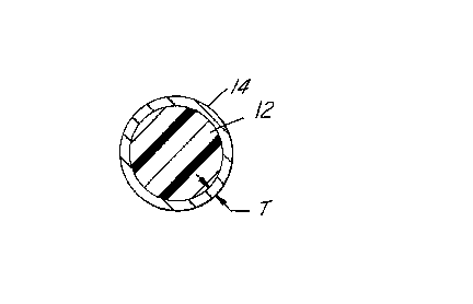
FIGURE lA is a cross-sectional view of a strand of mesh
material as shown in Figure 1, the view taken along line lA-lA in Figure
1 and in direction of the arrows;
FIGURE 2 depicts a spacecraft showing use of the present
invention on a reflector;
FIGURE 3 is a graph indicating the free space reflectivity
of a homogeneous surface as a function of surface resistivity;
CA 02210229 1997-07-11
_g_
FIGURE 4 is a graph showing the predicted
inherent PIM reduction between different materials;
FIGURE 5 is a graph showing the predicted
inherent PIM reduction for a nickel Aracon mesh;
FIGURE 6 is a graph showing the measured RF
reflectivity and through loss for a nickel Aracan mesh;
and
FIGURE 7 is a graph showing an inherent PIM
comparison between the present invention and a known
gold-molybdenum mesh.
Best Models) For Carrying Out The Invention
Turning now to Figure 1, there is shown a PIM-
protective mesh material 10 in accordance with the
present invention. The mesh material 10 includes a
plurality of base material fibers 12 woven into a fabric
mesh.
The base material 12 for the mesh is prefera-
bly a dielectric fiber, such as Kevlar°. A conductive
material 14, such as nickel or equivalent material, is
applied to the dielectric fibers of the mesh 10. This
is shown in Figure lA. The thickness of the conductive
material is adjusted to regulate the final conductivity
of the reflective surface to a pre-specified range which
reduces PIM while at the same time maintains a high
degree of RF reflectivity. The present invention
provides a deployable reflector mesh with acceptable
reflectivity, weight, mechanical, thermal, and light
transmission properties. At the same time, the inven-
CA 02210229 1997-07-11
_g_
tion reduces the "inherent" (or self-contact) PIM
potential to a level that is incapable of substantially
affecting the performance of the satellite system. In
particular, the invention has the advantage that it
reduces the surface conductivity to limit the conducted
RF energy from self-generating excessive PIM, while
maintaining an overall surface conductivity sufficiently
high to retain a sufficient "free-space" RF reflect-
ivity.
In accordance with the present invention, the
metallized mesh 10 is capable of reflecting a minimum of
97% of the RF energy while at the same time reducing the
"inherent" PIM (or self-PIM) by at least -40 dB.
Preferably, the invention reduces the inherent PIM
between -2 to -70 dB and more preferably -3 to -55 dB.
The present invention can be applied to the
diplexed L-band reflector in known spacecraft. The use
of the present invention on an antenna reflector is
shown in Figure 2. The invention substantially reduces
the risk of in-orbit PIM on PIM-sensitive programs.
This allows for greater freedom of use and reduced test
and re-work time during spacecraft development and
build-outs.
As shown in Figure 2, an antenna 20 is con-
nected by an arm or boom 22 to a spacecraft or satellite
body 24. When the antenna 20 is unfurled, the reflector
28 forms a parabolic structure. A plurality of radial
ribs 26 are deployed in a elliptical configuration
forming a parabolic-shaped reflector dish 28. The
metallic mesh material 10 is attached to the ribs 26.
CA 02210229 1997-07-11
-10-
When the antenna is deployed, the mesh is stretched in
a concave shape inside the parabolic dish forming the
reflector for the antenna. The radial ribs are thin and
flexible to support the mesh fabric and maintain the
parabolic contour. The ribs can be made of metal or a
composite material.
A feed 30 for the antenna is positioned on the
spacecraft body 24. The feed has an array of antenna
feeds or cups.
When the spacecraft or satellite is transport-
ed into orbit, the antenna is folded into a smaller
package. This is shown in phantom lines and designated
by the numeral 20'. Once the spacecraft is positioned
in space, the antenna 20 is unfurled into the shape and
position shown in Figure 2.
In the preferred embodiment of the invention,
the metallized reflector mesh at L-band comprises a
woven 0.125 inch tricot cellular mesh of nickel-plated
Aracon fibers. Aracon is a fiber made by the DuPont
Corporation and consists of a 55 Denier Kevlar~ thread
composed of 24 x 0.0006 inch filaments in a 0.004 fiber
size. In the Aracon process, each of the Kevlar~
filaments is individually and uniformly plated with
nickel. In order to achieve the desired mesh surface
resistivity, the thickness of the plating is specified
in terms of linear resistivity (ohms per foot) of the 55
Denier fiber.
CA 02210229 1997-07-11
-11-
The conductivity of the nickel plating is such
that the surface resistivity of the 55 Denier, tricot
mesh can be designed to fall within the desired PIM
reduction range. The predicted inherent PIM reduction
of 0.125 Aracon mesh material is shown in Figure 5. The
PIM reduction shown in the curve 36 indicates the
reduction of "saturated" PIM as a function of the
surface resistivity of the preferred mesh configuration.
In this regard, the PIM reduction is normalized to the
saturated PIM potential of a perfect conducting surface
such as aluminum or gold.
Figure 3 is a graph indicating the free space
reflectivity of a resistive surface. The graph shows
the reflective loss of a homogeneous resistive surface.
The curve 40 shows the reflected loss in dBs as a
function of the surface resistivity in ohms per square.
Spacecraft radio frequency (RF) reflector losses are
normally minus 0.1 dB or less. Surfaces with losses
between -0.1 dB and -0.5 dB may be useful in special
applications. Surfaces with losses greater than -0.5 dB
probably would not be practiced in most applications.
Inherent (self-contact) PIM reduction is
possible with resistivities greater than 0.1 ohm/square
for highly conductive surfaces - such as aluminum or
gold. Thus, the range of resistivities between 0.1 ohms
/square and 10 ohms/square are practical for both refle-
ctivity loss and PIM reduction. In accordance with the
present invention, the range of resistivity is between
0.01 and 10 ohms per square and preferably between 1-2
ohms per square. By balancing the factors between PIM
and reflectivity loss, a balance can be made to substan-
CA 02210229 1997-07-11
-12-
tially reduce the PIM risk while maintaining a satisfac-
tory RF reflectivity.
Figure 4 is a graph or chart illustrating a
comparison of inherent PIM reduction and surface resis-
tivity for different materials. The comparison is made
between a homogeneous surface of highly conductive
metals such as aluminum, gold or silver and a mesh
surface made of nickel or nickel-coated. The Y-axis is
PIM amplitude normalized to the worst case level of an
aluminum, gold or silver PIM source. The X-axis is the
surface resistivity, in ohms/square, of a surface
constructed of the specified materials.
Curve 50 demonstrates the predicted PIM
response of an aluminum surface. Curve 52 demonstrates
the predicted PIM response of a nickel mesh surface.
The chart demonstrates a benefit of PIM reduction in
both materials between the values of 0.1 ohms/square and
10 ohms/square surface resistivity. The nickel-coated
mesh surface (52) produces less PIM than the aluminum
surface (50) at lower resistivities and the aluminum
surface produces less PIM at the higher resistivities.
Figure 4 shows that although both materials
are useful as low PIM, RF reflective surfaces in the
range of resistivities between 0.1 - 10 ohm/square, the
nickel mesh surface (52) is particularly useful in very
low PIM, RF reflector applications. This is due to its
inherently low PIM response in the "lower" resistivity
ranges and results in a unique combination of low
inherent PIM response and low reflectivity loss. The
CA 02210229 1997-07-11
-13-
useful range of surface resistivities for a nickel mesh,
as shown in Figure 4, is 0.01 - 10 ohm/square in reflec-
tor applications.
As indicated above, Figure 5 illustrates the
predicted inherent PIM reduction for nickel Aracon mesh.
As shown, the mesh material has excellent PIM response
in the entire 0.01 - 10 ohm/square range of resistivit-
ies.
An Aracon mesh, in accordance with the above-
stated preferred embodiment, was electrically tested.
The surface resistivity measured between 2.1 ohms per
square and 2.5 ohms per square. The graph shown in
Figure 6 shows the measured RF reflectivity and through
loss. As shown in Figure 6, the dB loss is shown as a
function of radio frequency in gigahertz (GHz).
An "inherent" PIM comparison was also made on
the Aracon mesh in order to compare it with a known
gold-molybdenum mesh. The results of this comparison
are shown in Figure 7. The curve indicating the worst
case seventh order of inherent PIM in dBm relative to
the transmitted flux density (in mw/cm2), the gold-
molybdenum mesh curve, as indicated by the reference
numeral 60. In contrast, the curve utilizing the
present invention is shown by the reference numeral 62.
Thus, as shown in Figure 7, the present invention
secures a significant reduction over known metallic mesh
layers used for RF reflector surfaces.
CA 02210229 1997-07-11
-14-
In accordance with the present invention, the
low PIM reflective surface can be made from a nickel
metal materials, either of a radial nickel material or
a coated nickel material. In addition, the low PIM
reflective surface can be made of other metal materials,
such as aluminum, gold, silver or copper, and be depos-
ited as a thin film on a dielectric substrate, such as
Mylar, Kapton, a plastic material, or the like. The
thin film could be vacuum deposited on the surface, or
be applied in any other conventional manner.
The material with the inventive surface
thereon has preferred use as a reflector for a space-
craft antenna, but it also can be used for other reflec-
tors or reflector-type surfaces. The material can
either be a solid surface or a mesh of some type and the
key is to control the thickness of the metallized layer
in order to control the range of resistivity to maintain
a lower PIM response. As indicated above, the range of
resistivity is preferably 0.01 to 10 ohms per square.
When the metal material is plated, the thick-
ness, thus the surface resistivity, is controlled by the
plating thickness. When the metal material is formed as
a thin film, the thickness and thus the surface resis-
tivity is controlled by the deposition thickness. The
layer can be a single homogeneous reflective layer, a
metallized grid, a metallized balloon and the like.
CA 02210229 1997-07-11
-15-
While the best modes for carrying out the
invention have been described in detail, those familiar
with the art to which this invention relates will
recognize various alternative designs and embodiments
for practicing the invention as defined by the following
claims.