Language selection

Search

Patent 2210543 Summary

Third-party information liability

Some of the information on this Web page has been provided by external sources. The Government of Canada is not responsible for the accuracy, reliability or currency of the information supplied by external sources. Users wishing to rely upon this information should consult directly with the source of the information. Content provided by external sources is not subject to official languages, privacy and accessibility requirements.

Claims and Abstract availability

Any discrepancies in the text and image of the Claims and Abstract are due to differing posting times. Text of the Claims and Abstract are posted:

  • At the time the application is open to public inspection;
  • At the time of issue of the patent (grant).
(12) Patent: (11) CA 2210543
(54) English Title: CONNECTOR ASSEMBLY AND POWER CONTACT ELEMENT
(54) French Title: ENSEMBLE DE CONNECTEURS ET ELEMENT DE CONTACT DE PUISSANCE
Status: Expired and beyond the Period of Reversal
Bibliographic Data
(51) International Patent Classification (IPC):
  • H01R 12/52 (2011.01)
(72) Inventors :
  • CHAMPION, PATRICK (France)
  • MORLION, DANNY (Belgium)
  • PANIS, WERNER (Belgium)
  • THENAISIE, JACKY (France)
  • VAN KOETSEM, JAN PETER KAREL (Belgium)
  • JONCKHEERE, LUC (Belgium)
(73) Owners :
  • FRAMATOME CONNECTORS INTERNATIONAL
  • FRAMATOME CONNECTORS INTERNATIONAL
(71) Applicants :
  • FRAMATOME CONNECTORS INTERNATIONAL (France)
  • FRAMATOME CONNECTORS INTERNATIONAL (France)
(74) Agent: LAVERY, DE BILLY, LLP
(74) Associate agent:
(45) Issued: 2002-06-25
(22) Filed Date: 1997-07-16
(41) Open to Public Inspection: 1998-02-02
Examination requested: 1999-05-19
Availability of licence: N/A
Dedicated to the Public: N/A
(25) Language of filing: English

Patent Cooperation Treaty (PCT): No

(30) Application Priority Data:
Application No. Country/Territory Date
FR96/09817 (France) 1996-08-02

Abstracts

English Abstract


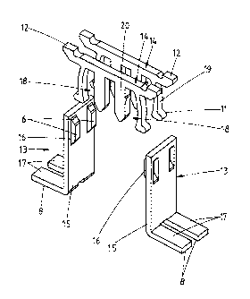
A connector assembly comprises a first connector
(1) and a second connector (2) adapted to be mated with the
first connector. Each connector has two spaced rows of
contact elements (4,10) arranged at a given pitch, each of
the contact elements having a contact face (6). In the first
connector (1) at least two adjacent contact elements (4) of
one row of contact elements are made integral as one first
power contact element (13) having two contact faces (6) at
the given pitch. In the second connector (2) at least one
contact element (10) of one row of contact elements can be
made integral with an opposite contact element (10) of the
other row of contact elements as one second power contact
element (14).


French Abstract

Un ensemble de connecteurs comprend un premier connecteur (1) et un deuxième connecteur (2) conçu pour s'accoupler avec le premier connecteur. Chaque connecteur a deux rangées espacées d'éléments de contact (4,10) disposés à un écartement donné, chacun des éléments de contact ayant une face de contact (6). Dans le premier connecteur (1), au moins deux éléments de contact (4) adjacents de l'unedes rangées d'éléments de contact sont combinés en un premier élément de contact de puissance (13) ayant deux faces de contact (6) à l'écartement donné. Dans le deuxième connecteur (2), au moins un élément de contact (10) d'une rangée d'éléments de contact peut être combiné avec un élément de contact opposé (10) de l'autre rangée d'éléments de contact pour former un deuxième élément de contact de puissance (14).

Claims

Note: Claims are shown in the official language in which they were submitted.


THE EMBODIMENTS OF THE INVENTION IN WHICH AN EXCLUSIVE
PROPERTY OR PRIVILEGE IS CLAIMED ARE DEFINED AS FOLLOWS.
1. Connector assembly, comprising a first connector
and a second connector adapted to be mated with said first
connector, each connector having two spaced rows of contact
elements arranged at a given pitch, each of said contact
elements having a contact face, characterized in that in
said first connector at least two adjacent contact elements
of one row of contact elements are made integral as one
first power contact element, having two contact faces at
said pitch.
2. Connector assembly according to the preamble of
claim 1, characterized in that in said second connector at
least one contact element of one row of contact elements is
made integral with an opposite contact element of the other
row of contact elements as one second power contact element.
3. Connector assembly according to claims 1 and 2,
wherein in said first connector each row of contact elements
has at least two adjacent contact elements made integral as
one first power contact element with two adjacent contact
faces in said pitch in each row, said first power contact
elements lying opposite one another, and wherein in said
second connector at least two adjacent contact elements of
one row of contact elements are made integral with
corresponding contact elements of the other row of contact
elements to obtain two adjacent second power contact
elements, said two second power contact elements lying at
locations corresponding to the locations of the contact
faces of the opposite first power contact elements.
4. Connector assembly according to claim 1, 2 or 3,
wherein each contact element of the first connector
comprises a first leg and a second leg joining said first leg,
wherein said first leg is provided with a contact portion
having said contact face and projecting with respect to said
first leg, said contact portion being formed out of said
first leg, wherein in each first power contact element the

first legs of said two adjacent contact elements are made
integral as one leg.
5. Connector assembly according to claim 1, 2 or 3,
wherein each contact element of the second connector
comprises a mainly n-shaped part with a first leg, a second leg
and an intermediate section interconnecting said first and
second legs, wherein said first leg is made as a contact
spring and said second leg is made as a fastening element
for fastening the contact element in a connector housing,
wherein in each second power contact element the
intermediate sections of said two opposite contact elements are
interconnected.
6. Power contact element, comprising one leg with
two contact portions each having a contact face, and two
further legs joining said one leg and having a width less
than half the width of said one leg.
7. Power contact element, comprising two mainly
n-shaped parts with a first leg, a second leg and an
intermediate section interconnecting said first and second legs,
wherein said first leg is made as a contact spring and said
second leg is made as a fastening element for fastening the
contact element in a connector housing, the intermediate
sections of said two n-shaped parts being interconnected.

Description

Note: Descriptions are shown in the official language in which they were submitted.


CA 022l0~43 l997-07-l6
FR 1779-dV/jk (C 1767)
Connector assembly and power contact element
The present invention generally relates to a
connector assembly, for example a board-to-board connector
assembly, and to power contact elements to be used in such a
connector assembly.
In connector assemblies, in particular in board-to-
board connector assemblies, used in telephone and computer
systems for example, it is important to miniaturize the
connectors and contact elements. With increasing miniaturi-
zation, the size of the contact elements may become too
small to meet the power requirements of the electronic
components connected through the connector assembly.
It is a general object of the present invention to
provide a connector assembly wherein relatively high power
requirements can be met despite the small size of the
contact elements used and the small pitch of the contact
elements.
According to the invention a connector assembly is
provided, comprising a first connector and a second connec-
tor adapted to be mated with said first connector, each
connector having two spaced rows of contact elements arran-
ged at a given pitch, each of said contact elements having a
contact face, characterized in that in said first connector
at least two adjacent contact elements of one row of contact
elements are made integral as one first power contact
element, having two contact faces at said pitch.
In an alternative embodiment, in said second
connector at least one contact element of one row of contact
elements is made integral with an opposite contact element
of the other row of contact elements as one second power
contact element.
In this manner a miniaturized connector assembly
can be provided wherein high power requirements can be met.

CA 02210~43 1997-07-16
The invention also provides a first power contact
element, comprising one leg with two contact portions each
having a contact face, and two further legs joining said one
leg and having a width less than half the width of said one
leg.
Further, the invention provides a second power
contact element, comprising two mainly n-shaped parts with a
first leg, a second leg and an intermediate section inter-
connecting said first and second legs, wherein said first
leg is made as a contact spring and said second leg is made
as a fastening element for fastening the contact element in
a connector housing, the intermediate sections of said two
n-shaped parts being interconnected.
The invention will be further explained by referen-
ce to the drawings in which embodiments of the connectorassembly and power contact elements according to the inven-
tion are shown.
Fig. 1 is a perspective view of an embodiment of
the connector assembly according to the invention, wherein
the first and second connectors are shown separately from
their top side.
Fig. 2 is a perspective view of the connector
assembly of Fig. 1, wherein the connectors are mated.
Fig. 3 shows a cross-section of the connector
assembly of Fig. l, wherein the first and second connectors
are mated and wherein the housing of one of said connectors
is partially cut-away.
Fig. 4 is a perspective view of four power contact
elements of the connector assembly of Fig. 1.
Fig. 1 shows a connector assembly comprising a
first connector 1 and a second connector 2 adapted to be
mated with the first connector 1. The connector 1 includes a
first housing 3 having two rows of first contact elements 4
arranged at a given pitch, said rows of contact elements 4
lying at a distance from each other along the longitudinal
walls 5 of the housing 3. Each contact element 4 comprises a
a contact face 6 projecting into a receiving space 7 of the

CA 02210~43 1997-07-16
first housing 3. The first contact elements 4 are disclosed
in a patent application of the same date of the same appli-
cant which is deemed to be incorporated here by reference.
As described in this application, each contact element 4 is
provided with two legs, one leg having said contact face 6
and the other leg having a connection terminal 8 for surface
mount connection to a contact area of a printed circuit
board not shown.
The second connector 2 comprises a second housing
with two rows of second contact elements 10 arranged at said
given pitch. These second contact elements 10 are also
described in a patent application of the same date of the
same applicant which is incorporated here by reference. As
described in this patent application each second contact
element 10 comprises a contact portion 11 projecting from
the corresponding longitudinal side of the second housing 9
and a connection terminal 12 for surface mount connection to
a contact area of a printed circuit board not shown.
For mating the connectors 1 and 2, the connector 2
is inserted into the receiving space 7 of connector 1 as
shown in Fig. 2. In this mated position of the connectors 1,
2, corresponding contact elements 4 and 10 are interconnec-
ted. The contact elements 4, 10 are for example arranged at
a pitch of 1 mm. The height of the first housing 3 may for
example be 5 mm and the height of the second housing may for
example be 2,4 mm. It will be understood that with such
dimensions, the size of the contact elements may be too
small to use the contact elements for power connections.
In the connector assembly described, the connectors
1, 2 can still be used for power connections by incorpora-
ting special power contact elements 13 in connector 1 and
special power contact elements 14 in connector 2. The power
contact elements 13, 14 are shown in detail in Figs. 3 and
4.
As shown in these Figs. 3 and 4, the first connec-
tor 1 is provided with two first power contact elements 13,
one power contact element 13 in each row at opposite loca-

CA 02210~43 1997-07-16
tions. Each power contact 13 comprises a leg 15 with two
contact portions 16 each having a contact face 6. Two
further legs 17 join the leg 15 and each have a width less
than half the width of the leg 15. Each leg 17 has a connec-
tion terminal 8.
Further, each power contact 14 comprises two mainly
n-shaped parts 18, each part 18 having a leg 19 made as a
contact spring and having the contact portion 11. Further,
each n-shaped part 18 has a fixation leg 20 with a cam for
locking the contact element 14 in the second housing 9. The
legs 19, 20 are interconnected by an intermediate section
having an extension with the connection terminal 12. The
intermediate sections of both n-shaped parts 18 are inter-
connected.
In this manner a power connection through four
first contact elements 4 and four second contact elements 10
is obtained. It will be understood that different combina-
tions of power contact elements 13 and 14 are possible. For
example, providing one power contact element 14 will result
in a power connection through two first contact elements 4
and two second contact elements 10. Further it is possible
to combine three or more adjacent first contact elements 4
into one power contact element 13.
The invention is not restricted to the above-
described embodiment which can be varied in a number of wayswithin the scope of the claims.

Representative Drawing
A single figure which represents the drawing illustrating the invention.
Administrative Status

2024-08-01:As part of the Next Generation Patents (NGP) transition, the Canadian Patents Database (CPD) now contains a more detailed Event History, which replicates the Event Log of our new back-office solution.

Please note that "Inactive:" events refers to events no longer in use in our new back-office solution.

For a clearer understanding of the status of the application/patent presented on this page, the site Disclaimer , as well as the definitions for Patent , Event History , Maintenance Fee  and Payment History  should be consulted.

Event History

Description Date
Classification Modified 2024-09-17
Inactive: IPC deactivated 2011-07-29
Inactive: IPC expired 2011-01-01
Inactive: IPC from MCD 2006-03-12
Inactive: First IPC derived 2006-03-12
Time Limit for Reversal Expired 2003-07-16
Letter Sent 2002-07-16
Grant by Issuance 2002-06-25
Inactive: Cover page published 2002-06-24
Pre-grant 2002-03-26
Inactive: Final fee received 2002-03-26
Notice of Allowance is Issued 2001-10-12
Letter Sent 2001-10-12
Notice of Allowance is Issued 2001-10-12
Inactive: Approved for allowance (AFA) 2001-10-03
Amendment Received - Voluntary Amendment 1999-09-16
Letter Sent 1999-06-14
Request for Examination Received 1999-05-19
Request for Examination Requirements Determined Compliant 1999-05-19
All Requirements for Examination Determined Compliant 1999-05-19
Inactive: Office letter 1998-07-08
Appointment of Agent Request 1998-05-21
Revocation of Agent Request 1998-05-21
Application Published (Open to Public Inspection) 1998-02-02
Inactive: Multiple transfers 1998-01-06
Inactive: IPC assigned 1997-10-09
Classification Modified 1997-10-09
Inactive: IPC assigned 1997-10-09
Inactive: First IPC assigned 1997-10-09
Inactive: Courtesy letter - Evidence 1997-09-30
Inactive: Filing certificate - No RFE (English) 1997-09-24
Filing Requirements Determined Compliant 1997-09-24
Application Received - Regular National 1997-09-23

Abandonment History

There is no abandonment history.

Maintenance Fee

The last payment was received on 2001-06-11

Note : If the full payment has not been received on or before the date indicated, a further fee may be required which may be one of the following

  • the reinstatement fee;
  • the late payment fee; or
  • additional fee to reverse deemed expiry.

Patent fees are adjusted on the 1st of January every year. The amounts above are the current amounts if received by December 31 of the current year.
Please refer to the CIPO Patent Fees web page to see all current fee amounts.

Fee History

Fee Type Anniversary Year Due Date Paid Date
Application fee - standard 1997-07-16
Registration of a document 1998-01-06
Request for examination - standard 1999-05-19
MF (application, 2nd anniv.) - standard 02 1999-07-16 1999-05-20
MF (application, 3rd anniv.) - standard 03 2000-07-17 2000-05-19
MF (application, 4th anniv.) - standard 04 2001-07-16 2001-06-11
Final fee - standard 2002-03-26
Owners on Record

Note: Records showing the ownership history in alphabetical order.

Current Owners on Record
FRAMATOME CONNECTORS INTERNATIONAL
Past Owners on Record
DANNY MORLION
JACKY THENAISIE
JAN PETER KAREL VAN KOETSEM
LUC JONCKHEERE
PATRICK CHAMPION
WERNER PANIS
Past Owners that do not appear in the "Owners on Record" listing will appear in other documentation within the application.
Documents

To view selected files, please enter reCAPTCHA code :


To view images, click a link in the Document Description column. To download the documents, select one or more checkboxes in the first column and then click the "Download Selected in PDF format (Zip Archive)" or the "Download Selected as Single PDF" button.

List of published and non-published patent-specific documents on the CPD .

If you have any difficulty accessing content, you can call the Client Service Centre at 1-866-997-1936 or send them an e-mail at CIPO Client Service Centre.


Document
Description 
Date
(yyyy-mm-dd) 
Number of pages   Size of Image (KB) 
Representative drawing 2002-05-20 1 9
Representative drawing 1998-02-24 1 8
Description 1997-07-15 4 181
Drawings 1997-07-15 3 65
Abstract 1997-07-15 1 19
Claims 1997-07-15 2 84
Filing Certificate (English) 1997-09-23 1 165
Reminder of maintenance fee due 1999-03-16 1 111
Acknowledgement of Request for Examination 1999-06-13 1 179
Commissioner's Notice - Application Found Allowable 2001-10-11 1 166
Maintenance Fee Notice 2002-08-12 1 177
Correspondence 1998-05-20 46 1,499
Correspondence 2002-03-25 1 33
Correspondence 1997-09-29 1 32
Correspondence 1998-07-07 2 9
Correspondence 1998-07-07 2 10
Fees 2001-06-10 1 40
Fees 1999-05-19 1 44
Fees 2000-05-18 1 40