Note: Descriptions are shown in the official language in which they were submitted.
CA 02210547 2000-12-18
1
A MICROWAVE VCO HAVIW(i REDUCED SUPPLY VOLTAf3E
Related Patents
This application is related to Applicant's U.S.
Patents 5,483,195 issued January 9, 1996; 5,420,538 issued
May 30, 1995; 5,371,475 issued December 6, 1994; 5,185,581
issued February 9, 1993; and 5,172,076 issued December 15,
1992.
Field of the Invention
This invention relates to linear amplifiers
incorporated into variable delay, low noise, high frequency
voltage controlled oscillators and particularly such
oscillators having reduced power supply requirements.
Background
With the advent of cellular radio telephone
distribution systems and the growing information era, the
importance of VHF and UHF personal communication systems has
grown. Implicit in this is the requirement for low cost
integrated solutions for clock recovery and analog UHF signal
processing. A major subcomponent of such communication
systems is the voltage controlled oscillator (VCO) which must
operate at UHF frequencies, at very low noise (fitter).
Currently, integrated solutions for the UHF oscillator are
sought for cost reasons.
Tf...: ...... T ... ~
In Applicant's prior U.S. patents, 5,172,076 and
5,185,581, small signal, voltage controlled oscillators
constructed with differential amplifiers are disclosed. These
VCO's, which are capable of operation to 1 GHz, can generate
up to about 0.15V peak to peak while providing a measured
noise fitter which is typically about 5 ps rms, or 0.005 Unit
Intervals (UI). A UI is the rms fitter divided by the
oscillator period. For many applications a fitter of
approximately 0.01 UI is adequate but for future
CA 02210547 2000-12-18
2
analog/digital converter techniques, fitter of 0.001UI at lGHz
or better will be required. This represents a required
improvement of 14 dB over that which is achieved by the
aforementioned prior patents. The present invention relates
to a VCO which addresses this requirement, while having lower
power supply requirements than Applicant's prior system as
described in U.S. Patent 5,483,195.
Summary of the Invention
It is an object of the present invention to provide a
linear amplifier which generates low noise at microwave
frequencies.
It is a further object of the invention to provide a
low noise, voltage controlled oscillator from a pair of
interconnected linear amplifiers.
It is yet a further object of the invention to
provide a voltage controlled oscillator having a high degree
of linearity at high signal levels.
It is a still further object of the invention to
provide the aforementioned advantages with a low power supply
voltage (3.3V).
In accordance with a first aspect of the present
invention there is provided a transconductance amplifier
having a variable delay. The amplifier comprises a linear
amplifier having three bipolar differential pairs, each having
a constant current source and a gain linearizing offset
provided by ratioed input emitter followers and associated
current mirrors. The differential pairs provide a
differential output. The transconductance amplifier
also has an auxiliary amplifier in parallel with the
linear amplifier, the auxiliary amplifier having first,
second and third differential pairs, each having a
CA 02210547 2000-12-18
3
constant current source. The auxiliary amplifier provides a
differential tuning current. A tuning control circuit
receives the differential tuning current and provides a tuning
output.
In a preferred embodiment each current source for the
differential pairs in the linear amplifier provides a greater
current than the current sources for differential pairs in the
auxiliary amplifier. The ratio of the two currents determines
the portion of the output current which goes to the tuning
circuit and hence controls the tuning range.
In accordance with a second aspect of the present
invention there is provided a transconductance amplifier
having a second linear amplifier in parallel with the first
linear amplifier and the auxiliary amplifier. Additionally,
the tuning circuit comprises four differential pairs wherein
differential tuning current from the auxiliary amplifier is
provided to two of the tuning differential pairs and the
current from the second linear amplifier is provided to the
other two tuning differential pairs. The four differential
pairs each with ratioed emitters combine to form a linear
tuning arrangement.
In a preferred embodiment the feedback current is
summed with the main current in a tapped load resistance.
In accordance with a further aspect of the
invention there is provided a voltage controlled oscillator
having a pair of transconductance amplifiers interconnected
such that the positive and negative outputs of the first
amplifier are connected to the positive and negative
inputs respectively of the second amplifier while the
negative output of the second amplifier is connected
to the positive input of the first amplifier and the
CA 02210547 2000-12-18
3a
positive output of the second amplifier is connected to the
negative input of the first amplifier. A 90° phase shift
exists between the outputs of each amplifier.
In accordance with a yet further aspect of the
invention, there is provided a transconductance amplifier
having a variable delay, the amplifier comprising: a linear
amplifier comprising first, second and third differential
pairs, each of the first - third.differential pairs including
first and second bipolar transistors, each of the first -
third differential pairs having a constant current source,
differential output being generated in response to the outputs
of the firs t - third differential pairs; first offset voltage
means for providing a gain linearizing offset to the first
bipolar transistor of the first differential pair; second
offset voltage means for providing a gain linearizing offset
to the first bipolar transistors of the second and third
differential pairs; third offset voltage means for providing a
gain linearizing offset to the second bipolar transistors of
the first and third differential pairs; fourth offset voltage
means for providing a gain linearizing offset to the second
bipolar transistor of the second differential pair; and tuning
control means responsive to the linear amplifier,
characterized by that: the linear amplifier further comprises
fourth, fifth and sixth differential pairs, each of the fourth
- sixth differential pairs including first and second bipolar
transistors, each of the fourth - sixth differential pairs
having a constant current source; the first offset voltage
means provides the first bipolar transistors of the first
and fourth differential pairs with a gain linearizing
offset; the second offset voltage means provides the first
bipolar transistors of the second, third, fifth and sixth
differential pairs with a gain linearizing offset; the
third offset voltage means provides the second bipolar
transistors of the first, third, fourth and sixth
CA 02210547 2000-12-18
3b
differential pairs with a gain linearizing offset; the fourth
offset voltage means provides the second bipolar transistors
of the second and fifth differential pairs with a gain
linearizing offset; and the tuning control means provides a
tuning output in response to differential tuning current from
the fourth - sixth differential pairs of the linear amplifier.
In a preferred embodiment, each of the constant
current source for the first - third differential pairs
provides a greater current than each of the constant current
source for the fourth - sixth differential pairs. The ratio
of the current through each of the first - third differential
pairs and the current through the fourth - sixth differential
pairs is an integer, e.g., three. In the transconductance
amplifier, the linear amplifier further comprises seventh,
eighth and ninth differential pairs, each of the seventh -
ninth differential pairs including first and second bipolar
transistors. The first offset voltage means providing the
first bipolar transistors of the first, fourth and seventh
differential pairs with a gain linearizing offset. The second
offset voltage means providing the first bipolar transistors
of the second, third, fifth, sixth, eighth and ninth
differential pairs with a gain linearizing offset. The third
offset voltage means providing the second bipolar transistors
of the first, third, fourth, sixth, seventh and ninth
differential pairs with a gain linearizing offset. The fourth
offset voltage means providing the second bipolar transistors
of the second, fifth and eighth differential pairs with a gain
linearizing offset.
In accordance with a yet further aspect of the
invention, there is provided a voltage controlled
oscillator comprising first and second transconductance
amplifiers as defined in claim 1, with a positive output
of the first transconductance amplifier connected to a
CA 02210547 2000-12-18
3c
positive input of the second transconductance amplifier, a
negative output of the first transconductance amplifier
connected to a negative input of the second transconductance
amplifier, a positive output of the second transconductance
amplifier connected to a negative input of the first
transconductance amplifier and a negative output of the second
transconductance amplifier connected to a positive input of
the first transconductance amplifier.
In accordance with a yet further aspect of the
invention, there is provided a voltage controlled oscillator
comprising first and second transconductive amplifiers, with a
positive output of the first transconductance amplifier
connected to a positive input of the second transconductance
amplifier, a negative output of the first transconductance
amplifier connected to a negative input of the second
transconductance amplifier, a positive output of the second
transconductance amplifier connected to a negative input of
the first transconductance amplifier and a negative output of
the second transconductance amplifier connected to a positive
input of the first transconductance amplifier.
Brief Description of the Drawings
The invention will now be described in greater detail
with reference to the attached drawings wherein:
FIGURE 1 is a block diagram of a prior art two-stage
ring oscillator;
FIGURE 2 is a block diagram of an oscillator
including a tuning arrangement;
FIGURE 3 is a circuit diagram of a linear amplifier
according to the prior art;
FIGURE 4 is the amplifier of FIGURE 3 with a tuning
circuit according to the prior art;
CA 02210547 2001-04-05
4
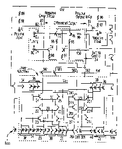
FIGURE 5 is a detailed circuit diagram of the 3.3
volt supply linear tunable gyrator transconductance amplifier
of the present invention;
FIGURE 6 is a detailed circuit diagram of a second
embodiment of the linear amplifier of the present invention;
and
FIGURE 7 is a graph of a typical spread of the tuning
characteristics of the oscillator.
Detailed Description of the Invention
In U.S. Patent 5,483,195 a VCO was described which
operates on the principle of a gyrator, having these
properties:
1. the gyrator consists of two transconductance
amplifiers connected in a loop with a wired 180
degree phase reversal at D.C.
2. the gyrator loop gain is controlled to be slightly
greater than unity at the gyrator resonant
frequency: This control is provided by an
automatic gain control system (AGC), so as to
maintain an oscillation at the gyrator resonant
frequency.
CA 02210547 1997-07-16
3. the gyrator has linear transconductors of the
design described in U.S. Patent 5,420,538 whose
linearity enables the creation of large resonator
5 Q factors at large signal levels, resulting in
low phase noise. Further, the linear
transconductors have variable transconductance
for the purpose of automatic gain control, which
control is obtained by variation of the amplifier
1o bias voltage.
4. the gyrator has a tuning mechanism which utilizes
a current feedback component of the output of
each of two transconductance amplifiers whose
i5 magnitude and phase are controlled to provide a
variable delay through the gyrator amplifiers by
means of vector summation of the feedback
currents with the output currents of the
associated amplifier. One form of the
2o transconductance amplifier is illustrated in
prior art Figure 4.
These objectives having been met, the properties of the
gyrator are described by Equation 1 and Equation 2 below.
25 Here Equation 1 describes the resonant angular frequency Z3o
in terms of the amplifier transconductance g",, the gyrator
capacitance C and a small second order term which is the
product of the gyrator loss admittance G and the amplifier
built-in-delay D. Equation 2 describes an orthogonal
3o condition which controls the resonator Q factor such that
the Q is infinite when this condition is satisfied. In
practice the delay D must be slightly greater than the
unity gain value to ensure oscillation.
35 Z5o - gm/(C+GD) . . . . . . . . . . . . (EQ 1)
D - G / ~t5o2C~ . . . . . . . . . . . . . ( EQ 2 )
CA 02210547 1997-07-16
6
All these, and other features are described in the
aforementioned U.S. Patent 5,483,195, to provide a low
phase noise voltage controlled oscillator having a
quadrature phase sinusoidal output with very low harmonic
distortion.
Experimental data shows that at frequencies of 2.4
GHz, a total harmonic distortion of -50dBc and better can
1o be maintained.
The present invention provides for all the
foregoing objectives to be obtained by modified
transconductance amplifiers requiring lower power supply
voltages than in U.S. Patent 5,483,195 and consequently to
provide for reduced power consumption. This is
accomplished by the amplifier circuit illustrated in FIGURE
5.
2o Specifically, FIGURE 1, taken from U.S. Patents
5,371,475, 5,172,076 and 5,185,581, illustrates a gyrator
comprised of two transconductance amplifiers with wired 180
degree phase reversal at D.C. FIGURE 2, taken from U.S.
Patent 5,483,195, illustrates a gyrator with feedback
current mechanism for tuning the gyrator resonant
frequency. FIGURE 3, taken from U.S. Patent 5,420,558,
illustrates a linear microwave transconductance amplifier
comprised of three differential pairs with small offset
voltages arranged at their inputs to create a linear
3o characteristic and a cascode output stage to enable
wideband microwave performance. FIGURE 4 illustrates a
linear transconductance amplifier suitable for operation at
supply voltage of 5 volts or greater according to U.S.
Patent 5,483,195. FIGURE 5 illustrates the new circuit of
the linear transconductance amplifier which is suitable for
operation at a supply voltage of 3.3 volts.
CA 02210547 1997-07-16
7
According to U.S. Patent 5,483,195, the circuit of
FIGURE 4 comprises three principal elements which are
illustrated by the dotted-line boxes. These principal
elements are a linear amplifier, a cascode phase splitter
and a tuning arrangement. The purpose of the cascode phase
splitter is two-fold: It provides the necessary cascode
stage for the linear amplifier in order to maximize the
bandwidth according to U.S. Patent 5,420,538: It also
provides a precise ratioed current division of the linear
to amplifier output, the smaller part of which is required by
the tuning arrangement. A disadvantage of the circuit as
illustrated in FIGURE 4 is that the tuning arrangement and
the cascode phase splitter appear in series cascode, thus
requiring a minimum 5 Volt supply.
According to the objectives of the present
invention, a reduction of the supply voltage is achieved by
eliminating the series cascode phase splitter of the
amplifier of FIGURE 4. This is achieved by augmenting the
linear amplifier with a built-in precisely ratioed phase
splitter and is illustrated in FIGURE 5. All the tuning
arrangements described in U.S. Patent 5,483,195 are
possible with this new arrangement, one of which is
illustrated in FIGURE 5 and corresponds to the similar
arrangement of FIGURE 4. Thus in this discussion, no
further reference to the tuning arrangement is necessary.
The linear amplifier of FIGURE 5 provides a main output
through cascode transistors 561 and 581 and an auxiliary
ratioed, lower, output directly to the tuning arrangement.
3o Thus there is no series cascode amplifier between the
auxiliary output and the tuning arrangement. This
arrangement is possible without degrading the performance
of the amplifier since the tuning arrangement also performs
the function of a cascode output stage.
The linear amplifier of FIGURE 5 is similar to
that of FIGURE 4 in that the two arrangements have
CA 02210547 1997-07-16
8
identical input circuits which provide the necessary offset
voltages required for linearity: This is provided by
transistors 34,35,36,37,38,39,40 and 41 using. the same
nomenclature in both figures. As described in U.S. Patent
5,420,538, the required offset voltages are obtained by the
ratios of the transistors 35:34, 36:37, 38:39, 41:40
which, according to the prior art, is specified as 3:1 for
optimum linearity. It was particularly specified in U.S.
Patent 5,420,538 that this ratio is required to be an
integer value due to the lithographic restriction
associated with minute microwave transistors.
With reference to FIGURE 4, the linear amplifier
output comprises three differential pairs whose outputs are
connected in parallel, namely, transistor pairs (20,21),
(22,23) and (24,25). Associated with these differential
pairs are current sinks 26,30 and 28 respectively. These
transistor differential pairs also appear in the new
arrangement of FIGURE 5, with the same nomenclature:
2o However the associated three current sinks now each consist
of three transistors in parallel, again with the same
nomenclature 26,30 and 28. In addition in FIGURE 5,
another auxiliary amplifier output stage is added,
comprising differential transistor pairs (201,211),
(221,231) and (241,251) and these have associated single
transistor current sinks 261, 301 and 281. In a typical
embodiment it can be specified that three times as much
current flows through the main amplifier output compared to
the auxiliary amplifier output due to the size of current
3o sinks 26,30 and 28. Thus the ratio of the current mirror
sizes which serve the main and auxiliary amplifiers
determines the proportion of the amplifier output current
which is fed to the tuning arrangement, and hence according
to U.S. Patent 5,483,195, this precisely controls the
tuning range. This ratio may be adjusted according to the
particular tuning range required. Two additional features
of this arrangement are to be noted, being properties of
CA 02210547 1997-07-16
9
the variable transconductance amplifier of U.S. Patent
5,420,538: the linearity of the main and auxiliary outputs
is not dependent upon the ratio of the above current sinks:
also the main to auxiliary output current ratio remains
constant as the AGC adjust the bias voltage of the
amplifier.
With reference to FIGURE 5, the illustrated
gyrator linear transconductance amplifier with tuning
1o control has a reference voltage which is derived by means
of a single diode drop (approximately 0.85 volts at 27°C)
from the positive power supply. The voltage at the
emitters of the cascode amplifier transistors 561 and 581
are thus two diode drops from the positive power supply.
Since the collectors of the linear amplifier are thus held
substantially constant, the emitters of the differential
pairs may be biased at approximately three diode drops from
the positive power supply. This means that, with a
standard 3.3 volts power supply, the current sinks of the
linear amplifier output stages are biased at a collector
emitter voltage of slightly less than one diode drop. This
is sufficient for their operation as current sinks under
the control of the AGC. In addition, in a particular
embodiment of this invention, these current sinks may be
augmented with a small amount of emitter degeneration,
according to standard practice, to improve the matching of
these current sinks. Alternatively, in a BiCMOS
technology, these current sinks could be implemented as
NMOS transistors with degeneration resistors: such NMOS
3o transistors can operate with lower drain voltages than the
equivalent bipolar transistors and so permit yet lower
supply voltages.
Yet another alternative version of the tuning
arrangement is possible while meeting all of the objectives
of the foregoing circuits. As noted in prior art, emitter
degeneration resistors are present in the tuning
CA 02210547 1997-07-16
arrangement of FIGURE 5 for the purpose of decreasing the
noise gain of the tuning transistors of FIGURE 5: these
resistors however impair the linearity of the translinear
tuning arrangement. An alternative arrangement is
5 illustrated in FIGURE 6. In this case, an additional
linear amplifier consisting of three differential pairs
(242,252), (222,232), (202,212) has been added to the
tuning arrangement to provide yet an additional pair of
output currents on nodes 563,583. The bias currents of
1o these three differential pairs are the same as those of the
three differential pairs (241,251), (221,231), (201,211),
and are typically of smaller value than the bias currents
of the main amplifier differential pairs (24,25), (22,23),
(20,21) by a predetermined ratio R. The ratio R determines
the maximum frequency range over which the oscillator can
be tuned, independent of processing variations and
temperature (as before). The additional linear amplifier
permits four pairs of differential pairs (A1,A2,A3,A4) each
with ratioed transistor emitters of 4:1 to be combined in a
linear tuning arrangement. It can be shown that the VCO
gain resulting from this arrangement is substantially
constant, independent of process variations and
temperature. A graph of a typical spread of the tuning
characteristics for fast, typical and slow processes is
shown in FIGURE 7. The frequency shift due to the bipolar
transistor variation is less than two percent over the
usable tuning range. The mode of operation of this linear
tuning arrangement can be understood as follows. U.S.
Patent 5,420,538 has described how two differential pairs
3o arranged in parallel input and output connections and with
emitter ratios of 1:4 and 4:1 respectively can constitute a
linear amplifier for input signal levels below a certain
value independent of the value of the equal differential
pair tail currents. In FIGURE 6, differential pairs
(A1,A2) constitute such a linear amplifier: also
differential pairs (A3,A4) constitute a second linear
amplifier. These two linear amplifiers are arranged in the
CA 02210547 1997-07-16
11
output circuits of linear amplifiers (241,251), (221,231),
(201,211) and (242,252), (222,232), (202,212) so as to form
a linear four quadrant mixer. Thus the magnitude of the
tuning control inputs linearly controls the magnitude of
the quadrature feedback currents, resulting in the linear
characteristics of FIGURE 7. Finally the noise
contribution of differential pairs (A1,A2,A3,A4) is less
than that of a simple Gilbert cell without degeneration
resistors due to two factors: a 3dB noise factor
to improvement results from the parallel combination of the
pairs of differential amplifiers: also, the noise power
delivered to the VCO load is reduced by about l2dB due to
the reduced gain of the amplifier. Total theoretical
improvement is about l5dB.
According to the objectives of this invention, a
new linear transconductor has been achieved which
replicates the properties of the transconductor described
in U.S. Patents 5,483,195 and 4,420,538, while at the same
2o time requiring substantially less voltage from the power
supply for normal operation. This results in a nominal 33
percent power saving, as well as conforming to the accepted
3.3 volt standard power supply voltage.
Additional features of the present invention are
identical to those of U.S. Patent 5,483,195, namely the
provision of tapped input resistors which also form the
load resistors of the other gyrator associated amplifier.
As determined by the aforementioned U.S. patents, these
3o tapped load resistors can have different tap ratios for the
two amplifiers, so as to provide the gyrator with two port
gain. This, according to the prior art, is useful for
providing multiple gyrator configurations.
Although specific embodiments of the invention
have been illustrated and described it will be apparent to
one skilled in the art that variations and alternatives to
CA 02210547 1997-07-16
12
these embodiments are possible. It is to be understood,
however, that such variations and alternatives may be
within the scope of the invention as defined by the
appended claims.