Note: Descriptions are shown in the official language in which they were submitted.
CA 022l0879 l997-07-l8
W O 97/19578 1 PCT~B96/01204
Circuit a~ n~ement
The invention relates to a circuit arrangement for operating a discharge
lamp with a high r~uellcy current comprising
- input terminals for connection to a source of low frequency supply voltage,
- rectifier means coupled to said input terminals for rectifying said low frequency
supply voltage,
- a first circuit comprising a series arrangement of first unidirectional means,
second unidirectional means and first capacitive means coupled to a first outputterminal N3 of said rectifier means and a second output terminal N5 of said
rectifier means,
- inverter means shunting said first c~p~itive means for generating the high
frequency current,
- a load circuit comprising a series arrangement of inductive means, second
c~p~citive means and means for applying a voltage to the discharge lamp, said
series arrangement connP~cting a terminal N1 of said inverter means to a
terminal N2 between the first unidirectional means and the second unidirectionalmeans, and
- a second circuit comprising third capacitive means and connecting terminal N2
to terminal NS.
Such a circuit arrangement is known from US 5,404,082. The known
circuit arrangement is very suitable to be powered from a regular mains supply generating
e.g. a supply voltage having an r.m.s. voltage of 230 Volt and a frequency of 50 Hz. The
known circuit arrangement has a relatively high power factor that is realized with compara-
25 tively simple means. A draw~ack of the known circuit arrangement is, however, that the
total harmonic distortion of the current that is drawn from the source of }ow frequency
supply voltage increases strongly if the means for applying a voltage to the discharge lamp
does not comprise a transformer and the lamp voltage is re]atively high. In case for in.ct~nce
the supply voltage has an r.m.s. voltage of 230 Volt, the harmonic distortion increases
CA 022l0879 l997-07-l8
W O 97/19578 2 PCT~B96/01204
strongly for a lamp voltage higher than a~lu~imately 70 Volt. It be mentioned that a similar
problem exists even for discharge lamps having a much lower values of the lamp voltage in
countries like for tn~t~nce the U.S.A. where the supply voltage has an r.m.s. voltage of only
120 Volt. This harmonic distortion can be decreased by incol~ul~ing a transformer in the
S means for applying a voltage to the discharge lamp. In case, however, the lamp voltage is
relatively high and the means for applying a voltage to the discharge lamp comprises a
transformer equipped with a primary winding and a secondary winding provided with
terminals for lamp connection, both the primary winding and other components comprised in
the load circuit and the inverter have to conduct a relatively large current. This relatively
10 large current can shorten the life of the circuit arrangement or makes it nececc~ry to
rlimPn~ion the circuit arrangement in accordance with this relatively large current, which is
en~ive. Another drawback of the known circuit arrangement is that it is often rlecesc~ry to
incl~ a frequency modulator in the circuit arrangement to modulate the frequency of the
high frequency current generated by the inverter means to correct for amplitude modulations
15 in this high fre~uency current and to control the crest factor of the lamp current at a value
less than approximately 1.7.
It is an object of the present invention to provide a circuit arrangement,
20 that causes relatively little harmonic distortion of the low frequency supply current, while the
circuit arrangement is also capable of operating discharge lamps having a relatively high
lamp voltage without the drawback of components comprised in the load circuit and the
inverter having to conduct a relatively large current during lamp operation.
A circuit arrangement according to the invention is for this purpose
25 char~.-t~ri7çcl in that the first output terminal N3 of the rectifier means is connected to a
terminal N4 between the second unidirectional means and the first capacitive means by
means of a third circuit compri~ing a series arrangement of third unidirectional means and
fourth unidirectional means and a terminal N7 between said third unidirectional means and
said fourth unidirectional means is connected to a terminal N6 that is part of the load circuit
30 by means of a fourth circuit and in that the neither the first circuit nor the third circuit
comprises inductive means.
During operation of the circuit arrangement the fourth circuit couples
power from terminal N6 to terminal N7. It has been found that this power feedb~ck that is
re~lized with relatively simple means causes a substantial decrease in harmonic distortion
CA 02210879 1997-07-18
W O 97/19578 3 PCT~B96/01204
when compared with the harmonic distortion caused by the known circuit arrangement.
Correspondingly the power factor increases subsf~nti~lly with respect to the power factor of
the lmown circuit arrangement. Surprisingly, despite the feedback realized by means of the
fourth circuit, in a circuit arrangement according to the present invention the current
5 cQn~ucte~ by conlponents compn~l in the load circuit and the inverter is relatively small,
even in case the means for applying a voltage to the discharge lamp comprises a transformer.
For this reason it is not nec~ ry to ~imçn~ion the inverter and the load circuit for a
relatively large current and the load circuit and the inverter circuit can therefore be realized
with relatively cheap components. Furthermore it has been found that it is possible to
10 dispense with a transformer in the load circuit of a circuit arrangement according to the
invention and keep the harmonic distortion at a relatively low level at the same time, even in
case the lamp voltage of the discharge lamp operated with the circuit arrangement is
relatively high. In case the load circuit does not comprise a transformer, the amplitude of the
current that flows through components of the inverter means and the load circuit during
operation is further decreased with respect to circuit arrangements according to the invention
compricing a transformer in the load circuit. Another ill~po~ t advantage of a circuit
arrangement according to the invention is that a frequency modulator for mod~ ting the
frequency of the high frequency current can also be dispensed with, since it was found that
the amplitude of the high frequency current generated by a circuit arrangement according to
~0 the invention is not strongly modulated and therefore the crest factor of the lamp current is
relatively low. Both the modulator and more particularly the transformer are relatively
eYren~ive components so that the possibility to dispense with both in a circuit arrangement
according to the invention is another reason why the circuit arrangement according to the
invention has a relatively simple configuration and is therefore relatively inexpensive.
It be mentioned that a circuit arrangement comprising a double power
fe~clb~ck similar to the double power feedback in a circuit arrangement according to the
present invention has been disclosed in EP 679046-Al. In the circuit arrangement disclosed
in EP 679046-A1 the improvement of the power factor is mainly effected by making use of a
storage coil. Such storage coil is a rather expensive component. In a circuit arrangement
according to the present invention a high power factor is achieved without making use of a
storage coil. For this reason the functioning of a circuit arrangement according to the present
invention differs from that disclosed in EP 679~46-A1. Furthermore a circuit arrangement
according to the present invention offers a substantial advantage over the disclosure of EP
679046-A1 because in a circuit arrangement according to the invention the expensive storage
CA 02210879 1997-07-18
W O 97/19578 4 PCT~B96/01204
coil can be ~icpçnc~d with.
It has been found that a smooth operation of the circuit arrangement could
be realized in case the second circuit further comprises the first capacitive means.
A smooth operation of the circuit arrangement was also found for
S config~ tiQnc of the circuit ~ ~ n~em~o.nt wherein the fourth circuit comprises fourth
~itive means.
The unidirectional means preferably comprise diode means. The unidirec-
tional means are thus realized in a very simple way.
In a pl~fe,-cd embo-lirnent of a circuit arrangement according to the
10 invention the inverter means comprise a series arrangement of a first switching element,
t~lllinal N1 and a second switching element, and a drive circuit DC coupled to the switching
elPnlpntc for generating a drive signal for rendering the switching elements alternately
conducting and non-conducting. The inverter is thus realized in a relatively simple and
dependable way.
It has been found that the circuit arrangement according to the invention is
very suitable for oper~ling two discharge lamps in parallel. In a pre~lled embodiment of a
circuit arrangement according to the invention for operating two discharge lamps, the load
circuit comprises a further series arrangement of inductive means, capacitive means and
means for applying a voltage to a discharge lamp and a terminal N8 that is part of the further
20 series arrangement is conn~ct~l to terminal N7 by means of a fifth circuit. the fifth circuit
plc;r~l~bly comprises fifth c~p~itive means.
In a further ~ref~ d embodiment of a circuit arrangement according to
the invention terminal N4 is connected to terminal N7 by a circuit comprising a switching
element S and a control circuit coupled to a control electrode of switching element S for
25 rendering switching element S conductive and non-conductive. The control circuit renders the
switching element S conductive when the lamp current is zero, for instance during preheating
of lamp electrodes or during ignition of the discharge lamp. An overvoltage over the first
c~pacitive means is thereby prevented. After the discharge lamp has ignited the control
circuit renders the switching element S non-conductive. The control circuit could for inct~ce
3~ comprise means for ~etecting a lamp current. It has been found, however, that a very simple
and dependable way to construct the control circuit is to equip said control circuit with
means for rendering the switching element S conductive and non-conductive in dependency
of the voltage over said first capacitive means.
CA 02210879 1997-07-18
W O 97/19578 5 PCT~B96/01204
Embo~imP-nt~ of the invent;on will be explained in more detail with
reference to a drawing, in which
Fig. 1 is a ~implififfi schem~tic diagram of a first embodiment of a circuit
arrangement according to the present invention with a discharge lamp LA connected to the
5 circuit arrangement;
Fig. 2 is a simr~ifiçd schematic diagram of a second embodiment of a
circuit arrangement according to the invention with two discharge lamps LAl and LA2
conn~ct~l to the circuit arr~n~ ent, and
Fig. 3 is a simplified sCll~m~tic diagram of a third embodiment of a
circuit arrangement according to the present invention with a discharge lamp LA connectell
to the circuit arrangement.
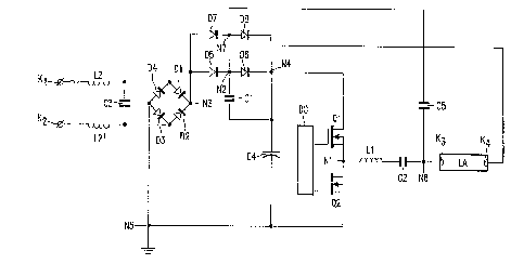
In Fig. 1 Kl and K2 are input terminals for connection to a source of low
fre~uency supply voltage. L2 and L2' are inductors that form an input filter together with
c~p~citQr C3. Diodes D1-D4 are rectifier means for rectifying said low frequency supply
voltage. In this embodiment diodes D5 and D6 form first and second unidirectional means
respectively. Capacitor C4 is first c~p~ci~ive means and forms together with diodes D5 and
D6 a first circuit. Switching elements Q~ and Q2 together with drive circuit DC form
inverter means. Drive circuit DC0 is a circuit part for generating drive signals for rendering
switching elem.ontc Q1 and Q2 conducting and non-conducting. Inductor L1, capacitor C2
and terminals K3 and K4 for connecting to a discharge lamp together form a load circuit. In
the embodiment shown in Fig. 1 inductor L1 forms inductive means, c~p~itor 2 forms
second capacitive means and terminals K3 and K4 for connecting to a discharge lamp form
means for applying a voltage to the discharge lamp. Capacitor C1 forms third capacitive
means. C~p~citor C1 and c~p~itor C4 together form a second circuit. Diodes D7 and D8
form third and fourth unidirectional means respectively. The series arrangement of diodes D7
and D8 forms a third circuit. Capacitor C5 forms fourth capacitive means and also a fourth
circuit.
Input terminals K~ and K2 are connected by means of a series arrange-
ment of inductor L2, capacitor C3 and inductor L2' respectively. A first side of capacitor C3
is connected to a first input terminal of the rectifier bridge and a second side of capacitor C3
is connected to a second input terminal of the rectifier bridge. A first output terminal N3 of
the rectifier bridge is connected to a second output terminal N5 of the rectifier bridge by
CA 02210879 1997-07-18
W O 97/19578 6 PCT~B96/01204
means of a series arrangement of diode D5, diode D6 and c~r~-itor C4. N2 is a common
~ al of diode D5 and diode D6. N4 is a common terminal of diode D6 and c~r~itQr C4.
Terminal N2 is col~ne~;led to terminal N4 by means of c~r~ritor C1. The series arr~ngPIn~nt
of diodes D5 and D6 is shunted by a series-arrangement of diodes D7 and D8. N7 is a
S common l~lllinal of diodes D7 and D8. Capacitor C4 is shunted by a series arrangement of
s.vi~ ing elPm~nt~ Q1 and Q2. A control electrode of switching element Q1 is connect~ to
a first output terminal of drive circuit DC. A control electrode of switching element Q2 is
conn~t~l to a second output terminal of drive circuit DC. N1 is a common terminal of
switching element Q1 and ~vilclling element Q2. Terminal Nl is connected to terminal N2
10 by means of a series arrangement of respectively inductor Ll, capacitor C2, terminal K3,
disch~g~ lamp LA and terminal K4. N6 is a common terminal of capacitor C2 and terminal
K3. Te~nmal N6 is connected to terminal N7 by means of capacitor CS.
The operation of the circuit arrangement shown in Fig. 1 is as follows.
When input terminals K1 and K2 are connected to the poles of a source of
lS a low frequency supply voltage, the rectifier bridge rectifies the low frequency supply
voltage supplied by this source so that a DC-voltage is present over c~p~citor C4 serving as a
buffer capacitor. Drive circuit DC renders the switching elements Ql and Q2 alternately
conducting and non-conducting and as a result a substantially square wave voltage having an
amplitude a~lo~imately equal to the amplitude of the DC-voltage over capacitor C4 is
20 present at terminal Nl. The substantially square wave voltage present at terminal N1 causes
an ~ltPrn~ting current to flow through inductor Ll and capacitor C2. A first part of this
alternating current flows through terminals K3 and K4, the discharge lamp LA and terminal
N2. The remaining part of this alternating current flows through capacitor CS and tel~ al
N7. As a result both at terminal N2 as well as at terminal N7 voltages having the same
25 frequency as the substantially square wave voltage are present. These voltages present at
terminal N2 and a terminal N7 cause a pulsatory current to be drawn from the supply voltage
source also when the voltage over capacitor C4 is higher than the momentary amplitude of
the rectified low frequency supply voltage. For this reason the power factor of the circuit
arrangement has a relatively high value and the total harmonic distortion of the supply
30 current is relatively low.
It be mentioned that similar results were obtained for a configuration of
the circuit arrangement slightly differing from the configuration shown in Fig. 1 in that
c~r~ r C1 connects terminal N2 to terminal NS instead of terminal N4. In this slightly
different configuration capacitor C1 forms third capacitive means and a second circuit.
CA 02210879 1997-07-18
W O 97/19578 7 PCT~B96/01204
In a pr~.tic~.~l realization of an embodiment as shown in Fig. 1, the
~lim~n.~is3ning was as follows: L1 = 905 ,uH, C5 = 5.6 nF, Cl = 18 nF, C4 = 11 ~F, C3
= 220 nP and C~2 = 180 nF, L2 = 1 mH and L2' = 1 mH. With this embodiment a low
~l~e~ule mercury discll~e lamp with a nominal power of 58 Watt was operated. The lamp
5 voltage of this lamp was 110 Volt. The frequency of the substantially square wave voltage
was ap~ ch~t~-ly 50 kHz and the power con~mçd from the low frequency supply voltage
source was 52.3 Watt. The low frequency supply voltage source was a European mains
supply supplying 230 Volts r.m.s with a frequency of 50 ~Iz. The lamp current was 452 mA
r.m.s. The lamp current crest factor was 1.43. The current through the switching elements is
10 591 mA rms. The total harmonic distortion was less than 10 %. It was found that when the
same low ~l~es~ure mercury discharge lamp was operated by means of a known circuit
arrangement as described in US 5,404,082 and equipped with a substantially identical input
filter, a transformer was needed in the load circuit to keep the total harmonic distortion level
at less than 10 %. When the r.m.s value of the current through the low pressure mercury
15 discl~al~;e lamp operated by means of the known circuit arrangement was approximately equal
to 452 mA, the current through the switching elements was approximately 798 mA r.m.s.
The r.m.s value of the current through the switching elements is thus 35 % higher than when
a circuit arrangement according to the invention is used.
The embodiment shown in Fig. 2 is to a large extent similar to the
20 embodiment shown in Fig. 1. Similar components and circuit parts are indicated with the
same reference signs in both figures. The load circuit of the embodiment of Fig. 2 comprises
a further series arrangement of inductive means capacitive means and means for applying a
voltage to a discharge lamp, formed respectively by inductor L3, capacitor C3 and terminal
KS and terminal K6. A discharge lamp LA2 is connected to terminals KS and K6. For clarity
25 the discharge lamp connected to terminals K3 and K4 is indicated by LA1 in Fig. 2.
Terminal K6 is connected to terminal K4. A terminal N8 between capacitor C6 and terminal
K5 is connectçd to a first side of capacitor C7. A further side of capacitor C7 is connected to
N7. Capacitor C7 forms in this embodiment both a fifth circuit and fifth capacitive means.
The operation of the embodiment shown in Fig. 2 is similar to that of the
30 embodiment shown in Fig. 1 and will not be described separately.
The embodiment shown in Fig. 3 differs from the embodiment shown in
Fig. 1 in that a switching element S connects terminal N4 to terminal N7. A control
electrode of switching element S is coupled to an output terminal of circuitpart ST. In Fig. 3
this is indicated by means of a dotted line. Capacitor C4 is shunted by a series arrangement
CA 02210879 1997-07-18
W O 97/19578 8 PCT~B96/01204
of resistor Rl and resistor R2. A common terminal of resistor Rl and resistor R2 is
connP~t~d to an input le~ inal of ~;ircuiL~ul ST. The embodiment shown in Fig. 3 is also
e~lui~ed with a means for preh~ing the electrodes of the discharge lamp La before
i~nitil n. These means comprise secon~ry windings L2 and L3 of coil L1 and c~r lt itors C6
5 and C7. Lach of the lamp electrodes is shunted by a series arrangement of a secondary
winding and one of the Ç~r~ itors C6 and C7.
The operation of the embodiment shown in Fig. 3 is as follows. Before
the disci~ar~e lamp La has i~nit~d, the lamp electrodes are preh~t~ during a predetermined
time lapse by renderin~ the ~witching elements conductive and non-conductive at a frequency
10 . at which the impedance of c~r~,itorS C6 and C7 is relatively low. Both during this
prehe~tin~ as well as during the ignition phase, the amplitude of the voltage over ~r~citor
C4 increases to a value that is higher than the value during stationary operation of the
discharge lamp. This higher amplitude is caused by the fact that the lamp current is zero
while power is fed back via capacitor C5. The voltage at the input terminal of circuitpart ST
15 is propollional to the voltage over c~r~citor C4. When the voltage over capacitor C4 reaches
a first predetermined value the circuit part ST renders switching element S conductive so that
diode D8 is shollcil~iuil~d whereby a further increase of the voltage over capacitor C4 is
prevented. When after the ignition of the dischal~e lamp the amplitude of the voltage over
~r~çitor C4 drops below a second predetermined value (lower than the first predelel..lined
20 value) the cir~;uil~all ST renders switching element S non-conductive so that power feedback
via ç ~r,~citor C5 is activated. The operation of the embodiment shown in Fig. 3 during
stationary operation is identical to that of the embodiment shown in Fig. 1 and will not be
further described.